a new True Random Bit Generator (TRBG) based on a time- delay sampled-data system is proposed. This new TRBG has both analog and digital parts, which ...
Throughput Enhancement for a New Time-delay Sampled-data System Based True Random Bit Generator Ramazan Yenic¸eri, Buse Ustao˘glu and M¨us¸tak E. Yalc¸ın Istanbul Technical University, Department of Electronics and Communication Engineering, Istanbul, Maslak, TR-34469, Turkey. E-mail:{yenicerir, ustaoglubu, mustak.yalcin}@itu.edu.tr Abstract—In this paper, a throughput enhanced version of a new True Random Bit Generator (TRBG) based on a timedelay sampled-data system is proposed. This new TRBG has both analog and digital parts, which provides the dynamic behavior and the sample and delay process, respectively. The simple system equations and the ease of implementation make this new TRBG very practical. The only required components for the implementation of the proposed system are commonly used Op Amps, resistors and capacitors with a chain of D-type flip-flops. The main contribution of this paper is the increase in random bit generation rate provided by two identical but unsynchronized cooperating circuits compared to the single circuit setup. As experienced, a 2.5 times greater random bit generation rate is achieved by this approach. In order to measure the statistical performance, the contemporary NIST 800-22rev1a Statistical Test Suite is used and it is experienced that the throughput enhancement is achieved with pass results from all these statistical tests.
I.
I NTRODUCTION
People are demanding more information secrecy in their daily electronic communication activities day by day. Currently, cryptography serves civil areas as much as the military desires. The confidence of the cryptographic encoders and decoders relies on the confidence of the key. Generation of the key requires true random number generators in order to generate actually unpredictable, unbiased, random bit strings. At the present time, it is known in literature that four methods exist for random bit generation. The first one is the amplification of a noise source [1]. The second one is the jittering oscillator sampling [2]. The third is the discrete-time chaotic maps [3] and the last method is based on the continuous-time chaotic oscillators [4], [5]. The statistical qualification, the throughput and the feasibility in IC implementation is the first three matter that all of the random number generators concern. Recently published time-delay chaotic circuits in [6] and [7] show that the time-delay blocks need effort to implement. Here, an efficient throughput enhancement is proposed which is based on a new statistically successful time-delay sampleddata system whose components are feasible to implement on the silicon [8]. This paper is organized in four sections. In Section II, the equations of the system model are given. The original circuit implementation is introduced in Section III and the enhancement is proposed in Section IV. Section V concludes the paper.
II.
T IME - DELAY S AMPLED - DATA S YSTEM E QUATIONS
The proposed system is a first-order nonlinear system in which a sampled, held and delayed feedback signal is put into use. The system equation is given by x(t) ˙ = −x(t) + αf (x(tk − τ )) ,
tk ≤ t < tk + Ts
(1)
where x is the analog state, α is the feedback weight, f is the nonlinear feedback function, τ is the delay amount applied to tk -th sample of the x, and Ts is the sampling period. Between tk and tk +Ts instants, the system evolves with constant x(tk − τ ) feedback signal which is sampled at tk and delayed while τ . The nonlinear function applied to the delayed signal is given by � −1 if |x| ≤ 1 f (x) = (2) 1 else. In this form, the system requires that x(tk − τ ) is present at t and the delay line on the feedback path should be delaying x which is continuous in amplitude. Designing analog circuitry to delay continuous amplitude signal is a troublesome process compared to designing the rest of the system. However, the system requirements become simpler when the delay is represented by the function TDelay [x(t)] = x(t − τ ).
(3)
The time invariance of the f (·) function enables the interchange of f (·) and TDelay [·]. Therefore, the system equation becomes x(t) ˙ = −x(t) + αTDelay [f (x(tk )], tk ≤ t < tk + Ts .
(4)
Thus, the feedback becomes a sampled and hold binary signal which is also delayed in time. The difference between delaying a continuous amplitude signal and a binary signal appears at the implementation of the system. The LC-ladder based delay block used for continuous amplitude signals are severe to implement in integrated circuits. But, binary signals have more chance to be successfully delayed by electronic devices. III.
C IRCUIT I MPLEMENTATION OF T HE T RUE R ANDOM B IT G ENERATOR
The advantage obtained by interchanging the nonlinear function and the delay function is sustained by using very
Fig. 1.
The schematic of time-delay sampled-data feedback true random bit generator circuit.
common digital electronic devices. To do this, the f (·) should be split into two functions, where f (x) = g(h(x)). h(·) and g(·) are described by ( VH if x > Vpos 0 if Vneg ≤ x ≤ Vpos h(x) = (5) VH if x < Vneg and
� g(h) =
VCC VEE
if h ≥ Vbias if h < Vbias
Fig. 2. The symbol of a Current Feedback Operational Amplifier (CFOA) and the defining signal on its terminals.
(6)
respectively. Here, Vpos and Vneg are the positive and negative threshold voltages which were 1V and −1V to implement Eq. 2. VH is the logic high level voltage which is valid in the delay line. Vbias is a small positive reference voltage. VCC is the positive and VEE is the negative supply voltages, which are +5V and −5V, respectively. A D-type flip-flop basically samples the binary data seen on its input at every triggering clock edge and holds this input at its output for one clock period. The cascaded N unit of synchronous D-type flip-flops again sample and hold the data at every one of two clock edges, either positive triggering edge or negative triggering edge. They moreover delay this input data for N × Ts seconds. Briefly, the chain which is constructed by a proper number of D-type flip-flops, implements the TDelay [h(x(tk ))]. When the g(·) function is applied to the output of the D-type flip-flop chain which is expressed in Eq. 7, the implementation of nonlinear feedback function is achieved. f (x(tk − τ ) = g (TDelay [h(x(tk ))])
(7)
As shown in Figure 2, D-type flip-flops, which are the sampling, holding and delaying devices, constitutes the digital part, and the nonlinear functions with x-integrator constitutes the analog part of the circuit. The analog part consists of discrete type of widely-used active components, such as AD844 and LM311, and passive components, such as resistors and a capacitor. A printed circuit board is designed and prepared for the analog part. Multi-turn potentiometers are used for high accuracy. AD844 is a current-feedback operational amplifier (CFOA), whose iz equals to the in for ideal case. Also, vo = vz and vn = vp for ideal CFOAs. The capacitor connected between the z terminal of the U2 CFOA and the ground in Figure 2 integrates iz , or in as well. On the other hand, the digital part is emulated by a lowcost Spartan-6 FPGA chip. The 1-bit wide flip-flop delay line becomes an on-chip RAM based 1-bit wide synchronous FIFO block for the emulation. The sampling rate Ts is 20ns for this FIFO structure and 655.36µs delay can be provided at most, using 32kb of RAM. Although this delay line length is enough for the realization, amount of bits are very insignificant compared to the 2088kb FPGA total on-chip block RAM. The
TABLE I.
T HE NIST 800-22 REV 1 A T EST S UITE ’ S SUMMARY 40M BIT STRING GENERATED BY SINGLE CIRCUIT.
RESULTS FOR A
Statistical Test Frequency BlockFrequency CumulativeSums CumulativeSums Runs LongestRun Rank FFT NonOverlappingTemplate OverlappingTemplate Universal ApproximateEntropy RandomExcursions RandomExcursionsVariant Serial Serial LinearComplexity
Fig. 3.
p-value 0.000000 0.000000 0.000000 0.000000 0.000000 0.000000 0.048716 0.000000 0.000000 0.000000 0.000000 0.000000 0.834308 0.017912 0.000000 0.509162 0.739918
Success Proportion 58/80 58/80 61/80 57/80 0/80 0/80 79/80 0/80 15/80 43/80 60/80 0/80 20/22 22/22 0/80 80/80 79/80
Result Fail Fail Fail Fail Fail Fail Fail Fail Fail Fail Fail Fail Pass Pass Fail Pass Pass
The strange attractor observed on the x(t) − x(t − τ ) plane.
FPGA also consists auxiliary modules for buffering recorded random-candidate bits, sending these bits to the computer and receiving commands from the computer. The statistical tests are applied on the computer. The success of this circuit as a TRBG is proved in our previous paper [8]. It is shown that a single circuit can generate bits at a rate of 20000 bps which pass the NIST 800-22rev1a Statistical Test Suite [9]. Nevertheless, the generated bits fail in the test suite when the bit capture period Tb is decreased from 50µs. For an example, the statistical test results are given in Table I for a 40Mbit record which has Tb = 20µs capture period. The complete parameter values of this record are given as VCC = 5V, VEE = −5V, Vbias = 0.5V, VH = 3.3V, Ts = 20ns, C = 5.6nF, R1 = 2.78kΩ, R2 = 5.78kΩ, Vpos = 1.12V, Vneg = −0.81V, and τ = 500µs. It also should be noticed that the system exhibits a strange attractor behavior in the x(t) − x(t − τ ) state space as shown in Figure 3. On the other hand, there should be a strong relation between the randomness of the generated bits and the non-periodicity of the phase portrait of this system. With given component values, the
time constant equals to 15.568µs which results in 10.23kHz cut-off frequency of passive RC filter connected to the U2 for x-integration. Observation on recorded x(t) data sampled with 1MHz shows that 99% of the signal energy is in 65kHz bandwidth. The next section proposes a solution to make the generated bits clearly pass the randomness tests by doubling the signal source with another circuit and utilizing this twin in an unsynchronized manner. IV.
U NSYNCHRONIZED B EHAVIOR OF T WO I DENTICAL C IRCUITS
Firstly, a second circuit which is identical to the first one is prepared. For the analog part, a new circuit board is printed, but the digital part is implemented next to the first one on the same FPGA. Figure 4 depicts the circuit pair with the common bit recording buffer. Here, the bits generated by each circuit are subjected to a logical ex-or operation. Hence, a statistically better stream is obtained from two bit streams. Still, the FPGA has a single bit record buffer. This buffer captures the output of the ex-or gate. The ex-or operation could be considered as a post-processing operation.
Fig. 4. The block diagram of the unsynchronized circuit pair, the ex-or gate and the bit recording buffer.
As expected, this new configuration obtains better NIST 800-22rev1a test results. The recorded 40Mbit strings with Tb = 20µs sampling period clearly pass the statistical tests. Table II shows the success in tests with numerical results for an example bit string. The similar successful statistical results are achieved with many bit strings recorded by the same setup. The predecessor of NIST test suite is the FIPS 140-1 tests. Exactly, the Poker sub-test of this old suite, which is an easily implementable fast statistical test, is applied primarily. The average Poker test results of single and double circuit setup for different bit sampling rates are given in Figure 6. The black horizontal line on the graph indicates the maximum Poker result to pass. When the second circuit is joined, better Poker results are achieved. In spite of good Poker results, the NIST tests’ results do not match at considerable lower sampling periods than ones indicated by vertical lines on the same figure. The relation between the success in NIST tests and other metrics should be analysed in the future works. Expanding the TRBG system from one to two first order nonlinear subsystems yields two continuous states (x1 (t),
TABLE II. RESULTS FOR A
T HE NIST 800-22 REV 1 A T EST S UITE ’ S SUMMARY 40M BIT STRING CO - GENERATED BY A PAIR OF CIRCUITS .
Statistical Test Frequency BlockFrequency CumulativeSums CumulativeSums Runs LongestRun Rank FFT NonOverlappingTemplate OverlappingTemplate Universal ApproximateEntropy RandomExcursions RandomExcursionsVariant Serial Serial LinearComplexity
p-value 0.941144 0.986869 0.739918 0.258961 0.484646 0.012650 0.764655 0.371101 0.023149 0.764655 0.275709 0.663130 0.407091 0.100508 0.764655 0.350485 0.141256
Success Proportion 79/80 77/80 79/80 79/80 78/80 78/80 79/80 79/80 77/80 80/80 79/80 78/80 35/36 35/36 77/80 79/80 79/80
Result Pass Pass Pass Pass Pass Pass Pass Pass Pass Pass Pass Pass Pass Pass Pass Pass Pass
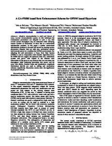
Fig. 6. The observed phase portrait of the two circuit system on x1 (t)−x2 (t) state space.
of the analog circuits and also the random bit generation rate as well. The recorded bit strings belonging to the single circuit case and to the twin circuit case is published on a web page with their statistical test results on the following address. http://www.gstl.itu.edu.tr/publisheddata.html R EFERENCES [1] Fig. 5. The average Poker Test results for 2µs ≤ Tb ≤ 60µs interval for single (red) and double (blue) circuit forms.
[2]
x2 (t)) and a 2D continuous state space. The unsynchronized behavior of the entire system can be observed by examining the trajectory of the system state in this state-space. Figure 6 shows the screen-shot of an analog oscilloscope which is depicting x1 (t) − x2 (t) space. The homogeneity and the symmetry of the trajectory in this state-space is clearly seen. The trajectory pattern can be observed as a qualitative analysis on the system behavior. The pattern in Figure 6 can be interpreted as a proof of unsynchronized and unbiased dynamic behavior which has positive contribution to the randomness. V.
[3]
[4]
[5]
C ONCLUSION
Using two identical time-delay sampled-data feedback systems as independent bit sources and combining their outputs using an ex-or gate increases the throughput by 2.5 times. The randomness of the generated bit strings are tested by the up-todate statistical test suite NIST 800-22rev1a. Exactly, increasing the number of unsynchronized circuits will yield much entropy, then better statistical characteristics, so the proposed system can be expanded by utilizing more identical subsystems to achieve higher random bit generation rates. It is also expressed that the proposed system can be easily integrated on a silicon chip, owing to the digital delay line and simple analog part. Decrease in the time constant value of the integrator and using faster operational amplifiers will widen the bandwidth
[6]
[7]
[8]
[9]
V. Bagini and M. Bucci, “A design of reliable true random number generator for cryptographic applications,” in Cryptographic Hardware And Embedded Systems, ser. Lecture Notes in Computer Science, C. K. Koc and C. Paar, Eds., vol. 1717. Springer-Verlag Berlin, 1999, pp. 204–218, 1st International Workshop on Cryptographic Hardware and Embedded System (CHES 99). B. Jun and P. Kocher, “The intel random number generator,” Cryptography Research, Inc., White Paper, April 1999. S. Callegari, R. Rovatti, and G. Setti, “Embeddable ADC-based true random number generator for cryptographic applications exploiting nonlinear signal processing and chaos,” Signal Processing, IEEE Transactions on, vol. 53, no. 2, pp. 793–805, feb. 2005. S. Ergun and S. Ozoguz, “Truly random number generators based on a non-autonomous chaotic oscillator,” AEU - International Journal of Electronics and Communications, vol. 61, no. 4, pp. 235–242, 2007. [Online]. Available: http://www.sciencedirect.com/science/article/ pii/S1434841106000720 V. Tavas, A. S. Demirkol, S. Ozoguz, A. Zeki, and A. Toker, “An ADC based random bit generator based on a double scroll chaotic circuit,” Journal of Circuits, Systems and Computers, vol. 19, no. 07, pp. 1621–1639, 2010. [Online]. Available: http://www.worldscientific. com/doi/abs/10.1142/S0218126610006918 A. Buscarino, L. Fortuna, M. Frasca, and G. Sciuto, “Design of timedelay chaotic electronic circuits,” Circuits and Systems I: Regular Papers, IEEE Transactions on, vol. 58, no. 8, pp. 1888–1896, 2011. V.-T. Pham, L. Fortuna, and M. Frasca, “Implementation of chaotic circuits with a digital time-delay block,” Nonlinear Dynamics, vol. 67, no. 1, pp. 345–355, 2012. [Online]. Available: http: //dx.doi.org/10.1007/s11071-011-9982-9 R. Yeniceri and M. E. Yalcin, “True random bit generation with timedelay sampled-data feedback system,” Electronics Letters, vol. 49, no. 8, April 2013. A. Rukhin, J. Soto, J. Nechvatal, M. Smid, E. Barker, S. Leigh, M. Levenson, M. Vangel, D. Banks, A. Heckert, J. Dray, and S. Vo, NIST Special Publication 800-22: A Statistical Test Suite for Random and Pseudorandom Number Generators, 1st ed., April 2010.