Laser Metrology and Inspection, Proc. SPIE, Vol. 3823, Munich, (1999), accepted for publication.
Time-of-flight range imaging with a custom solid-state image sensor R. Langea, P. Seitza, A. Bibera and R. Schwarteb a
b
Centre Suisse d’Electronique et de Microtechnique SA (CSEM), Badenerstrasse 569, CH-8048 Zurich, Switzerland
Universität-GH-Siegen, Institut für Nachrichtenverarbeitung (INV), Hölderlinstrasse 3, D-57068 Siegen, Germany ABSTRACT
A complete range camera system, working with the time-of-flight principle, is introduced. This ranging system uses modulated LEDs as active illumination source and a new lock-in CCD sensor as demodulator and detector. It requires no mechanically scanning parts because every pixel of the sensor contains a lock-in amplifier, enabling both intensity and range measurement for all pixels in parallel. Two such lock-in imagers are realized in 2.0µm CMOS/CCD technology, (1) a line sensor with 108 pixels and an optical fill factor of 100% and (2) a 64x25 pixel image sensor with 20% fill factor. The basics of time-of-flight ranging are introduced with a detailed description of the elements necessary. Shot noise limitation to ranging resolution is deduced and confirmed by simulation. An optical power budget is offered giving the relation between the number of photons in a pixel depending on the light source, the observed object, and several camera parameters. With the described lab setup, non-cooperative targets can be measured over a distance of several meters with a resolution of some centimeters. Keywords: Time-of-flight, 3D-measurement, range camera, CCD technology, lock-in technique, light modulation.
1. INTRODUCTION The amazing progress experienced in the past thirty years in the field of microelectronics, largely driven by the computer industry, is also at the heart of the multimedia revolution: Prices of solid-state imagers have dropped to such low levels that video cameras, camcorders and web cameras virtually have become household items. Yet, they can capture only a twodimensional projection of our three-dimensional world, often representing a serious deficiency in many practical applications such as safety, security, automotive applications, automatic manufacturing, etc. For this reason, a large number of threedimensional optical measurement techniques and so-called range cameras have already been developed, quite a few of which are described in References 1 and 2. These techniques essentially rely on three types of principles: Triangulation, such as in passive stereo 3 or in active phase-shifting moiré 4, Interferometry, either using a single wavelength for incremental 5 or multiple wavelengths for absolute distance measurements 6, Time-of-flight ranging, either using pulsed modulation 7 or continuous modulation 8 of the light source. Each of these fundamental techniques has profited in its own way from the advances made in microelectronics. While triangulation and interferometry saw more cost-effective implementations, their measurement accuracy was, however, not substantially affected. In the case of triangulation, the measurement range and precision is critically determined by the triangulation baseline. Obviously, miniaturization of the complete system leads to a reduced triangulation baseline and therefore to reduced accuracy. The precision in interferometry is basically given by the wavelength of the employed coherent light source, a parameter that cannot be influenced greatly. The situation is completely different for time-of-flight (TOF) range imaging techniques. They have not only become cheaper, smaller and simpler to realize but their measurement accuracy is also increasing steadily. It is the purpose of this paper to investigate the reasons for this development, to explore the physical and engineering limits, and to predict probable future progress in this field. In Section 2, the evolution in microelectronics is outlined, in view of advanced capabilities useful for improving TOF ranging. The basics of TOF distance measurement are summarized in Section 3. Section 4 contains the description of the lock-in CCD image sensor, the key element for the TOF distance imaging technique. A simple light power budget for the
1
Laser Metrology and Inspection, Proc. SPIE, Vol. 3823, Munich, (1999), accepted for publication.
prediction of maximum ranging distances is given in Section 5 and the complete TOF range camera architecture and its performance are described in Section 6. Conclusions and an outlook to what the future might bring in TOF range imaging are presented in Section 7, followed by the summary in Section 8.
2. ADVANCED MICROELECTRONICS FOR IMPROVED TIME-OF-FLIGHT RANGING
Minimum feature size [microns]
The advances in microelectronics rely on the amazing technological capabilities of the industry to reduce minimum feature sizes in integrated electronic circuits relentlessly, and to increase the size of the wafers that are produced at the same time. As an example, consider the evolution of minimum feature size illustrated in Fig. 1. Over the past thirty years, minimum geometries have steadily and quite predictably 10 been reduced by about 10% per year, representing an exponential size reduction. This implies five things: (1) More and more electronic circuits find place on the same silicon area, (2) reduced geometries mean (linearly scaled) smaller capacitances and 1 shorter interconnection lengths, leading to higher circuit speeds (under the assumption of identical charge/discharge currents), (3) smaller field-effect transistor gate capacitances allow better transistor noise performance, (4) a chip of constant size will not only contain more electronic circuits with much higher 0.1 functionality, it will be cheaper to produce because of the economy of scale, and (5) 1970 1975 1980 1985 1990 1995 2000 2005 2010 devices that rely on the diffusion of charge Year carriers (such as surface-channel CCDs) show a significant decrease in transport times Fig. 1: Evolution of the minimum feature size in silicon-based because the average diffusion time depends on semiconductor technology, featuring a quite predictable the square of the diffusion length 10. exponential shrinking of about 10% reduction per year. Full Based on this insight, we can now see why the TOF measurement principle can profit from the advances in microelectronics on many levels:
circles are values achieved by advanced manufacturing plants; open circles are predictions 9.
• Smaller imager chips imply smaller systems and lower cost. • Higher circuit and device speed leads to more accurate timing capabilities and therefore higher TOF distance resolution. • Higher circuit density implies a larger optical fill factor and therefore higher sensitivity TOF pixels. • More electronic circuitry enables more functionality (smarter pixels), more reliable and robust operation, and simpler, cost-effective overall system design • Lower transistor noise leads to more sensitive TOF range measurement systems with higher resolution and larger distance measurement ranges. It is obvious, therefore, that TOF range imaging profits much more from the continuing advances in microelectronics than any other optical distance measuring principle. Consequentially, steady improvements can be expected in the future. This basic assertion is at the heart of the work presented in the following.
3. TIME-OF-FLIGHT With the precise knowledge of speed of light 12,13 we can measure a distance by measuring the time that a light pulse needs to travel from an observed target to a reference point. In practice, the active light source and the receiver are located very close to each other. This facilitates a compact setup and avoids shadowing effects. The basic principle of a TOF-ranging system is shown in Fig. 2. A source emits a light pulse and starts a high accuracy “nanosecond stop watch”. The light pulse travels to the target and back. Reception of the light pulse by the detector mechanism stops the stop watch, which now shows the time
2
Laser Metrology and Inspection, Proc. SPIE, Vol. 3823, Munich, (1999), accepted for publication.
DISTANCE
transmitter
START
STOP
50
80 70
30
60
detector
ns
10 20
3D object
100
1m = 6.67ns
40
90
"ns stop watch"
receiver Fig. 2
Basic principle of a time-of-flight ranging system.
of flight of the light pulse. Considering the fact that the light pulse travels the way twice (forth and back) a measured time of 6.67ns corresponds to a distance of 1m. An essential property of this setup is the fact that emitter and detector are synchronous. At this point one can recognize a significant advantage of time-of-flight over a triangulation system: The TOF ranging technique does not produce incomplete range data (no shadow effects) because illumination and observation directions can be collinear. The basic problem of establishing a TOF-ranging system is the realization of the nanosecond stop watch. There are several methods differing in their needs for illumination source, receiver, and modulation signal. In the following subsections, the different possibilities of modulation signals as well as typical realizations for light sources and detectors with modulation and demodulation capability are introduced. MODULATION SIGNALS The type of modulation signal can generally be distinguished between (1) pulsed light, (2) continuously modulated light (CW-modulation) and (3) a combination of both. All these modes of operation have their specific advantages and disadvantages, which will be discussed in the following. 1.
Pulsed light operation, as illustrated in Fig. 2, is the most obvious method because the time of flight is measured directly. The advantage of using pulsed light is the possibility of transmitting a high amount of energy in a very short time. Thus a high short-term optical signal-to-noise ratio is attained while maintaining a low mean value of optical power. This is an important factor for eye safety, which is the limiting criterion for many measurement applications. Furthermore, it reduces the demand on a very high sensitivity and signal-to-noise ratio of the detector, thus enabling long distance measurements. It is, however, difficult to produce very short light pulses with fast rise and fall times. Such pulses are necessary to assure an accurate detection of the incoming light pulse, independent of the detection level.
2.
CW-modulation offers the possibility of using alternative demodulation and detection mechanisms as described below. A larger variety of light sources is available for this mode of operation because extremely fast rise and fall times are not required. Different shapes of signals are possible, including sine-waves, square-waves and also the repetition of pseudo noise words (PN modulation) offering the advantage of a very high peak in the autocorrelation function14. For CWmodulation generally the phase difference between sent and received signal is measured. As the modulation frequency is known, this measured phase directly corresponds to the time of flight, the quantity of interest. In contrast to the homodyne operation (only one frequency) which is described here, sinusoidal modulation offers the additional possibility of heterodyne operation15 (use of more than one modulation frequency).
3.
The combination of CW-modulation with pulsed operation combines their specific advantages: (1) better optical signalto-noise performance than available from pure CW-modulation, (2) increased eye safety due to a low mean value of optical power and (3) larger freedom in choosing modulators and receivers. Such a combination is, for example, a “pulsed sine” operation, i.e. a sequence of 1ms high power sine modulation followed by 9ms of optical dead time. This dead time can be used for post processing tasks.
3
Laser Metrology and Inspection, Proc. SPIE, Vol. 3823, Munich, (1999), accepted for publication.
TRANSMITTER: MODULATED LIGHT SOURCES AND ELECTRO-OPTICAL MODULATORS The emitted light can be modulated in several ways. The use of LEDs or lasers allows direct modulation of the light source by controlling the electrical current. Since the sent light does not have to be coherent or monochromatic, other light sources are possible, in combination with additional large aperture optical modulators such as Kerr cells 11, Pockels cells 11,15, mechanical shutters or liquid crystal shutters. Pulsed operation with fast rise and fall times is only possible with directly controlled laser sources which allow pulses of less than ten femtoseconds. 24 The different light sources and modulators can be characterized in terms of light intensity, cut-off frequency, linearity, wavelength, modulation depth (the ratio of signal amplitude to signal offset), eye safety properties, size and price. LEDs are relatively inexpensive. They can be modulated up to some 100MHz with a 100% modulation depth and a very high linearity. They are available for a wide range of wavelengths from blue (400nm) to the near infrared (1200nm) with an optical power of up to several milliwatts. 25 Lasers, even laser diodes, are much more expensive than LEDs and are often larger. However, they offer more optical power and are suited for operation up to some GHz, also at a wide range of wavelengths 25. Kerr cells are based on the quadratic electro-optic effect where the polarization of a polarized beam is rotated depending on the applied voltage. Together with a polarizer and a modulated control voltage of the cell, a polarized incoming beam can be modulated in intensity. Kerr cells can be used as modulators up to 10GHz but voltages as high as 30kV must be switched at this speed. 11 Pockels cells, making use of the linear electro-optic effect 11,19 (pockels effect), work very similarly and also require polarized light for operation. Their cut-off frequency of more than 25GHz is even higher than that of Kerr cells. The driving voltage requirements are a factor of 10 lower than for an equivalent Kerr cell. However, the Pockels cell still requires some kilovolts to switch from transparent to opaque mode. Therefore, the practical cut-off frequency, which is limited by the cell’s capacitance, reaches only several hundred MHz 25. Liquid crystal shutters are limited to some kHz of modulation frequency 25 and are therefore not suited for high-resolution measurement applications in the 10 meter range. An interesting alternative, however, might be the realization of a mechanical shutter. Miniaturized air turbines with a rotation speed of 427’000rpm have been reported 26. If one manages to rotate a light grating disc with such an air turbine, shutter frequencies as high as 1MHz might become possible. For example, a disc of 10cm diameter and a slot width of 1mm at the edge of the disc would contain about 150 slots. Such a disc would offer a 1x1mm2 shutter aperture while allowing 1MHz shutter frequency (=150*427000(1/min)/60(s/min)). RECEIVER: DETECTORS AND DEMODULATION The easiest way of realizing a TOF-receiver is to use any fast and sensitive electro-optical sensor as detector. The time of flight can then be determined as follows: a linear ramp is started synchronously with the transmission of a laser pulse. Once the laser pulse reaches the detector the rise of the ramp is stopped. The resulting amplitude is then proportional to the time of flight. The difficulty of this detection mechanism is the definition of a trigger level for the detector, because the amplitude of received light strongly depends on the distance and surface to measure. For 1D-TOF ranging systems high dynamic, high sensitivity PIN photo diodes or APDs (avalanche photo diodes) are used. PIN photo diodes have a very fast response. Typical cut-off frequencies are 10GHz and beyond. After the fast detection the modulated light, now converted to an electrical signal, is electrically demodulated leading to the desired phase difference between transmitter and receiver. APDs and photomultiplier tubes16 can be modulated in their sensitivity, enabling a direct demodulation or mixing of the incoming light. Today, products are offered with ±1.5mm accuracy for non-cooperative targets over a distance of 100 meters. 22 All these components only allow a 1D measurement. The operation of many such receivers in parallel appears to be impractical due to large size and enormous demand on additional electronics. Therefore, 2D depth profiles or 3D depth images can only be obtained from such 0D detectors by scanning the light beam over the observed surface. This, however, requires time, because every point has to be measured serially. It also requires mechanical scanners of very high precision. Those scanners are bulky, expensive, and sensitive against vibrations. A promising advance in 3D TOF-ranging is the use of large aperture optical modulators, such as Kerr cells or Pockels cells 15. Such devices can be used as demodulators in the receiver path taking over the time critical part of mixing. They enable the use of commercially available detector arrays (e.g. CCD or CMOS cameras) for the optical to electrical
4
Laser Metrology and Inspection, Proc. SPIE, Vol. 3823, Munich, (1999), accepted for publication.
conversion. There is no need for the detectors themselves to be very fast because they only integrate DC images containing the phase information (distance information respectively), amplitude information and offset information (background image). 15,17 The drawback of using large aperture optical modulators is their high price and enormous requirement on high voltage POLY1 POLY2 METAL1 SHIELD CONTACT VIA POLY2 METAL1 SHIELD CONTACT VIA POLY1 driving electronics (in case of Kerr cells photogate offset control gate dump gate and Pockels cells). An interesting dump pipeline CCD diffusion alternative is to use a two dimensional photomultiplier tube as optical transfer gates demodulator: the so called microchannel 17,18,25 plate (MCP) . A MCP can be output CCD switched on and off in less than 500ps 1 Pixel (1GHz modulation frequency). However, readout CCD those devices suffer from their relatively high price and, as for Pockels cells, a voltage amplitude of about 1000 Volts is necessary, requiring elaborate Fig. 3 Layout and architecture of previous lock-in sensors. Left: multitap electronics. sensor, Right: four-tap sensor. The shield mask in the upper images marks the light sensitive regions of the pixels. An even more complex and robust setup for a 3D ranging system can be realized by combining the 2D-demodulation and 2D-detection process in one device. The first such device, realized in CCD technology, was, however, not invented to be used in an optical ranging system but for a 2D-polarimeter19. For simplified 3D TOF measurement without mechanical scanners the lock-in CCD sensor was invented; this device is also realized in CCDtechnology. The CCD gates are arranged such that light generated charge carriers under the photo gate can be moved to four different storage sites (4-tap-lock-in sensor). 20,23 This allows fast sampling of incoming light. Thus, phase and amplitude of the modulated light can be calculated employing the rules of discrete Fourier transform. Even more sampling points can be stored in a multitap lock-in pixel. This allows the demodulation of more complex signals (for example pseudo random words) in parallel. However, the trade off for realizing a large number of storage sites in a pixel is the loss of optical fill factor: 0.5% for a multitap-lock-in pixel with 8 storage sites 21. The pixel layouts of the multitap- and the 4-tap-lock-in sensor are illustrated in Fig. 3. A related architecture, which is operated with modified sinusoidal control signals, is the photonic mixer device (PMD) 14. This device has a modified differential amplifier in every pixel, which integrates the sum and the difference of two demodulation currents, demodulated with 180° phase difference. µm 35µ
µm 40µ
A first 3D TOF-camera with 2D detector has recently been offered commercially 28. This system works as follows: A light pulse of some tens of nanoseconds is transmitted by a laser, and it synchronously starts the integration of a standard CCD camera. With the electrical shutter mechanism of the CCD camera, only a very short period of time (also some tens of nanoseconds) is integrated. Thus, depending on the distance of the targets, only a fraction of the light pulse arrives before the integration stops. Performing two calibration measurements, one without laser illumination, and one with non-pulsed, continuous laser illumination enables distance calculation. The drawback of this principle is that no repetitive integration is possible; the CCD has to be read out after every short time integration. This leads to a poor signal-to-noise ratio of the principle that can only be compensated by very high optical power of the laser. The power of laser sources, on the other hand, is limited by eye safety regulations.
4. LOCK-IN CCD SENSOR In the previous section, we have learned about the requirements for a 3D TOF-ranging system with 2D demodulation and detection. Now we will describe the lock-in CCD sensor as an example of a two-dimensional stop watch or, to be more precise, a two-dimensional phase meter. In order to simplify the understanding, we will use sinusoidal modulation signals to explain the principle of phase detection.
5
Laser Metrology and Inspection, Proc. SPIE, Vol. 3823, Munich, (1999), accepted for publication.
SAMPLING AND DISCRETE FOURIER TRANSFORM Fig. 4 shows the sinusoidal modulation signal. It contains three unknowns: offset, amplitude and phase (frequency is given). Therefore at least three sampling points per modulation period are necessary to completely reconstruct the signal. For higher measurement accuracy and a simpler evaluation algorithm it is, however, advantageous to use four instead of three sampling points. Following the rules of discrete Fourier transform one can calculate the three unknowns as follows: Phase:
ϕ = arctan
Amplitude:
A=
Offset:
a0 − a2 a1 − a3
(1)
f=20MHz, T=50ns
Popt
A
(a0 − a2)2 + (a1 − a3)2
(2)
4
a0 + a1 + a2 + a3 B= 4
a0
a1
a2
B
a0
a3
t
(3) Fig. 4
Sinusoidal modulation signal.
A fast sampling of the modulation signal enables the measurement of the signal phase, offset, and amplitude. The modulation frequency, which is determined by the maximum non ambiguous distance range (20MHz for 7.5m range) is, however, too high to use a standard CCD or CMOS-image sensor for the repetitive sampling process. The complete sensor would have to be read out within the modulation period time. Therefore, a new device is necessary, capable of repetitive accumulating charge of a selective time interval into a storage site within each pixel. REALIZATION AND LAYOUT One possible realization in CCD technology for such a pixel is illustrated in Fig. 5. Photoelectrons can either be integrated under the 5V biased integration gate or they are dumped to a diffusion, depending on the potential gradient within the semiconductor. This potential gradient can directly be influenced by the voltage applied to the light sensitive photo gates. The maximum transfer speed of this device is mainly limited by (1) slow thermal diffusion process, (2) the size of CCD gates, and (3) the capacitance of CCD gates. 1.
Typical doping concentrations of standard CMOS processes lead to an extension of the depletion layer of less than one µm into the semiconductor. Long wavelength light penetrates deeply into the semiconductor before generating electron hole pairs (about 20µm for 850nm: NIR). It can only be A1 detected if it reaches the depletion zone by thermal diffusion, a relatively slow statistical transport process.
2.
The only directed charge transport mechanism within a semiconductor is the movement of charge in an electrical field. The electrical field between two adjacent CCD gates (fringing field) is, however, restricted to a relatively small area (depends on the doping concentration of the semiconductor). For large photo gate lengths charge carriers see practically no electrical field at any place under the photo gate. Only near the edges of an adjacent photo gate biased at a different potential, electrical fields are present. Thus, for large photo gates, the thermal diffusion process again mainly influences the speed of charge movement. Therefore, for a fast movement of photoelectrons, the length of the photo gates has to be as small as possible. This measure is determined by the design rules of the technology and cannot be influenced by the designer.
3.
A1
t 0V
3V 0V
1.5V
0V 3V
5V
opaque layer CCD gates oxide substrate
High capacitance of the photo gates requires high current CCD gate drivers for fast operation. Fig. 5
6
5V
Potential
dump diffusion
A1 Architecture of lock-in pixel, cross section and potential distribution.
Laser Metrology and Inspection, Proc. SPIE, Vol. 3823, Munich, (1999), accepted for publication.
Examples of the pixel architecture described above are illustrated in Fig. 6. It shows two image sensors, a line sensor and an imager, both realized in Orbit 2.0µm CMOS technology with CCD option. Photo gates and Pixel storage are realized in CCD technique whereas the readout is realized with APS (Active Pixel Sensor) principle, i.e. every pixel has its own amplifier and can selectively be accessed with an address decoder. This offers higher readout flexibility.
µm 15µ
POLY1
POLY2
n+ diff.
POLY2
n+ diff.
METAL1
SHIELD
CONTACT
µm 15µ
CONTACT In contrast to previous lock-in 20,21,27 realizations now only Fig. 6 Realizations of lock-in imagers in one sampling point can be 2.0µm CMOS/CCD technology. Top: (repetitively) integrated and Micrograph and pixel-layout of 108 stored within a pixel at a time. pixel lock-in line sensor (100% fill This requires the serial factor, 16µm pitch). Bottom: 64x25 acquisition of four pictures, Pixel lock-in imager (20% fill factor, one for each sampling point. 25µm x 64µm pitch). These pictures have to be stored externally after being read out. Once these four sampling points have been acquired and stored, the phase (and hence the time of flight) can then be calculated for every pixel. The fact that the sampling points cannot be measured at the same time lowers the measurement accuracy for fast moving objects. The new layouts in Fig. 6 drastically increase the optical fill factor to 20% and 100% respectively compared to only 0.5% of the multitap lock-in device 21. Imaging TOF-measurements are possible only with these reasonable fill factors. Furthermore, like in References 14 and 20, the requirement of a fast charge transfer is satisfied by employing only three CCD gates. POLY1
METAL1
SHIELD
NON-IDEAL SAMPLING: INTEGRATION The equations given above ((1)-(3)) can directly be deduced from the discrete Fourier transform (DFT) with four coefficients. DFT, however, implies ideal sampling; i.e. the sampling points are not integrated but taken at only one point in time. In practice it is impossible to perform an ideal sampling process, the signal is always integrated. This is known as nonideal sampling process. It is obvious that for integration times much smaller than the signal period ideal sampling is nearly fulfilled and hence (1)-(3) can be used. In our optical lock-in application, however, this claim cannot be fulfilled. An integration time much shorter than the modulation period means that only a small fraction of the modulated light is used for the range measurement, leading to a bad signal-to-noise ratio. The extreme case, concerning the choice of integration time, is an integration time that equals the signal period. If that is the case all (non-ideal) sampling points become equal and the measured signal amplitude is zero, obviously a useless result. The integration of sampling points can be described as a convolution of an ideally sampled signal with a rect(t/∆t) function, where ∆t is the integration time. In the frequency domain this corresponds to a multiplication of the power spectrum of the ideally sampled signal with the power spectrum of the rect(t/∆t) –function, which is ∆t⋅sinc(f⋅∆t)= ∆t⋅sin(f⋅∆t) / (f⋅∆t). This has the following influences on the lock-in application: 1.) The integrative nature of practical sampling has no influence on the measured phase. The ideal sampling points a0..a3 in equation (1) can be replaced by the integrated values A0..A3 without causing an error. This is because the sinc-function is real and has no complex part; it has no influence on the phase spectrum.
7
Laser Metrology and Inspection, Proc. SPIE, Vol. 3823, Munich, (1999), accepted for publication.
2.) The measured amplitude is attenuated by the sinc-function compared to the real amplitude. Therefore using the measured values (non-ideal sampling) for equation (2) requires a correction factor of 1/(∆t⋅sinc(∆t/T)) to obtain the real signal amplitude. The equations can thus be rewritten for the integrated values A0..A4: ϕ = arctan
Phase:
A=
Amplitude:
δ ⋅ ∆t ⋅ sin δ B=
Offset:
A0 − A2 A1 − A 3
(A 0 − A 2)2 + ( A1 − A3)2 4
A 0 + A1 + A 2 + A 3 4 ⋅ ∆t
(4)
(5)
(6)
Where δ = π⋅∆t / T with sampling interval ∆t and modulation period T. 27 We are currently operating the lock-in sensor at a modulation frequency of 20MHz with a sampling interval of 25ns, i.e. half the modulation period. This leads to a decrease in the measured signal amplitude to 64% of the real amplitude but it reduces the speed requirements of driving electronics and control signals.
5. OPTICAL POWER BUDGET AND ESTIMATION OF RANGE RESOLUTION Since the time-of-flight principle uses active illumination, it is important to know the requirements for the power of the light source. For this purpose, two things have to be known: (1) how many photoelectrons per sampling point and pixel are necessary to achieve a certain range resolution? And (2), how much light power is necessary to generate that number of electrons? Both questions will be investigated and answered in this chapter. QUANTUM NOISE LIMITATION TO RANGING RESOLUTION The performance of solid state imagers is limited by noise. There are several different noise sources in both CCD sensors and photodiode arrays. The essential ones are electronic shot noise, thermal noise, reset noise, 1/f noise and quantization noise. All of these noise sources can be reduced or eliminated by different signal processing techniques, except shot noise. Therefore, we only investigate the influence of shot noise on the ranging accuracy in this section. Shot noise describes the statistical Poisson-distributed nature of the arrival process of photons and the generation process of electron-hole pairs. The standard deviation of shot noise is equal to the square root of the number of photons or photogenerated charge carriers. Following the rules of error propagation and considering that each of the integrated sampling points A0..A3 in equation (4) shows a standard deviation of sqrt(A0)..sqrt(A3) one obtains: Standard deviation of range error: L:
σd =
L
1 M ⋅ B+ . M 2 8 ⋅
(7)
non-ambiguity distance range;
M: measure for the modulation amplitude, (the number of photoelectrons per pixel and sampling point generated by incoming light of the modulated light source); B:
measure for the background light, (the number of photoelectrons per pixel and sampling point generated by incoming light of the scene’s background brightness). This value corresponds to B-A/2 in (5) and (6).
Choosing L=7.5m (i.e. f= 20MHz), M=10’000 electrons and B=100’000 electrons leads to a ranging accuracy of 8.5cm. This result was also confirmed by simulation of the shot noise influence on equation (4).
8
Laser Metrology and Inspection, Proc. SPIE, Vol. 3823, Munich, (1999), accepted for publication.
The range accuracy (7), which can only be improved by averaging, is the absolute limit of a lock-in range sensor working with four sampling points. In (7) only quantum noise is considered. All other noise sources and the efficiency of the demodulation process of the device are neglected. One can see from the equation that a large background illumination not only restricts the number of available quantization levels, but also drastically increases the quantum noise of the system. Background illumination can be reduced by measuring in the dark or by using spectral filters that only transmit the spectrum of the modulated light. From that point of view, lasers are advantageous over all other light sources due to their monochromatic nature. Since, generally, the optical power density on the illuminated scene increases with decreasing distance to the object, the ranging accuracy also increases for smaller distances (increase of M/B). This is an important fact for all navigation applications, where a high accuracy is only needed close to the target. OPTICAL POWER BUDGET
quantum efficiency
# electrons
# photons
energy of photon
Epixel energy per pixel
integration time losses of lens and filter
Plens optical power in front of lens D 2⋅ R
Pimage
pixel area, sensor area
optical power on sensor
Ppixel optical power on pixel
2
D: aperture of lens R: distance of object
The example given above says that for Pobject Plight source remission coefficient a given background level of 100’000 of object required optical power electrons per pixel and sampling point, optical power on object of light source (Lambert reflector) 10’000 signal electrons have to be generated, to obtain a ranging resolution of 8.5cm over a non- Fig. 7 Optical power budget: influence of light source, scene, and camera parameters. ambiguous distance range of 7.5 meters. Now we want to investigate which light power we need to achieve this. The number of generated electrons is related to the number of photons over the quantum efficiency of the imager. With the energy of one photon, the integration time, the size of light sensitive pixel area and the size of the complete sensor, one can calculate the total amount of optical power that has to appear on the sensor. Consideration of optical losses of the lens and filters leads to the power in front of the lens over the aperture area. If the observed object is a Lambert reflector one can calculate the optical power on the observed scene, which has to be a factor of (0.5⋅D/R)2 higher than the power in front of the lens (D: aperture of the lens, R: distance to target). With the remission coefficient of the object (value between zero and one, ρ=1 for a white sheet of paper), we can then calculate the power of the light source needed. These relationships are illustrated in Fig. 7 and summarized in the following formula: Ne ⋅ Required optical power of emitter:
N e: Asensor: Apixel: h: c:
number of electrons per pixel sensor area light sensitive area of pixel Planck’s constant speed of light
Popt,source =
ρ: D: R: klens: QE(λ):
A sensor ⋅h⋅c A pix
2
D ρ⋅ ⋅ k lens ⋅ QE(λ ) ⋅ λ ⋅ Tint 2⋅R
remission of object aperture of lens distance of object losses of objective and filters quantum efficiency
.
(8)
λ: wavelength of light Tint: integration time
To illustrate this equation, the following practical values are selected: A 3.8m diameter non-cooperative object with a remission coefficient of 0.2 is located in 5m distance. An accuracy of 8.5cm is required. (Tint=10ms, λ=620nm, f=20MHz, lens: f/1.6, 2.6mm, Apixel=12.5µm x 14.5µm). Assuming that the imaged area and the illuminated area are identical, one
9
Laser Metrology and Inspection, Proc. SPIE, Vol. 3823, Munich, (1999), accepted for publication.
obtains a light power of 5W that is required for the illumination of the object, i.e. a power density at the object of 440mW/m2. It is interesting to notice that a certain optical power density on the object always leads to the same number of electrons in the pixel, independent of its distance. If the same light power is used to illuminate an area of one square meter, once 5m away from the sensor, and once 50m away from the sensor, the number of electrons generated in one pixel stays the same. This is because the angle of view for the observation of a fixed area also decreases with the distance of the object. Hence, the illumination beam has to have a smaller divergence to illuminate the object in a greater distance with the same power density.
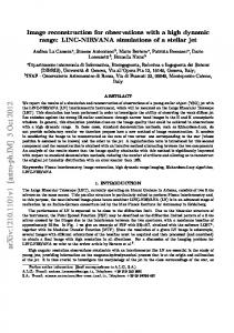
6. SYSTEM ARCHITECTURE, PERFORMANCE AND EXPERIMENTAL RESULTS As already mentioned, the lock-in sensors are realized in CMOS technology with CCD option. Gate voltages up to 10V have to be applied, depending on the pixel architecture. High-speed highFig. 8: Lab setup of 3D-camera demonstrator. current gate drivers are necessary because the CCD gates have to be charged and discharged with a frequency of some tens of megahertz. A typical capacitance value for the 25x64 pixel lockin device is 200pF for one CCD channel. An interesting and very powerful realization for such gate drivers is the use of 74AHCXX logic family ICs operated beyond specification at 10V. The 74AHC08, a quadruple 2-input positive AND in Advanced High Speed CMOS technology, has rise and fall times of less than 7ns for 220pF load and a voltage swing of 10V. This enables operation up to 50MHz. Additionally there are special powerful gate drivers commercially available. Currently we are using 2 Ampere CMOS gate drivers, with specified 10ns rise and fall times for 1000pF load. The often complex control signals for fast signal sampling and readout are generated by software as bit patterns, so called clock files. These can be loaded into a RAM-based sequencer over the parallel port of a PC. Such a sequencer is very flexible concerning modifications in the clocking scheme. An alternative is the use of a DSP. The light source consists of 16 high luminosity LEDs. We use a PPI (Parallel Port Interface) for the 12-bit A/D conversion. This is a flexible frame grabber, developed at CSEM, which can easily be connected to the parallel port of any PC. Fig. 8 shows a photograph of the latest lab-setup. In spite of limitations of the currently used sequencer and the relatively low optical light power, even this setup enables time-of-flight distance measurements of non-cooperative targets up to several meters with a resolution of about ±10cm. A measured profile is shown in Fig. 9.
7. OUTLOOK To improve the overall performance of the ranging camera we will, as a next step, increase the optical light power and integration time. This requires the realization of a new sequencer, preferably a DSP solution. Furthermore, we will perform a detailed investigation of the complete sensor performance concerning overall linearity of the amplifier stages, sensitivity to clock jitter, efficiency of temporal charge separation (sampling), and behavior at higher modulation frequencies. In order to increase the system performance and to benefit from the enormous improvements in microelectronics we will realize the future lock-in devices in 1m state-of-the-art CMOS technologies. It will be necessary therefore, first to investigate the possibilities of realizing charge transport in a pure CMOS process using surface-channel CCD principles. The use of smaller technologies principally allows adding additional functionality, like signal preprocessing, to Fig. 9: Measured profile, taken with 108 every pixel without losing too much fill factor. pixel lock-in line-sensor.
10
Laser Metrology and Inspection, Proc. SPIE, Vol. 3823, Munich, (1999), accepted for publication.
The realization of small CCD elements in a standard CMOS technology requires small gaps between the CCD gates instead of overlapping gates, causing a loss in performance. With the improvements in technologies these gaps between the gates can, however, be smaller and smaller (currently 0.5µm) so that comparably good performance can be expected for future designs. As described above, the movement of charge carriers from one CCD gate to another, in a non-CCD process with relatively high substrate doping, is mainly influenced by the thermal diffusion process and not by the existence of an electrical field. Since the time for charge transport due to diffusion depends quadratically on the length of the CCD gates, the overall speed of charge movement will increase with decreasing gate lengths. Additionally, the electrical field between the CCD gates will gain importance for the charge transport. An interesting alternative to the 2D-sampling/demodulation device introduced here would be the use of a sensitivity modulated array of avalanche photodiodes. Such a device is introduced in Reference 29. A general limiting factor of the maximum distance range is always the amount of light power received by the detector. Therefore the detector has to be as sensitive as possible. A way of increasing the sensitivity is to use microlenses for every pixel. Such microlenses enlarge the virtual fill factor. Another possibility of increasing sensitivity is to separate the light sensitive part from the readout- and post processing-part and to realize both in separate, vertically stacked layers. This is possible with a so-called photo-conversion layer, which can be deposited on top of a standard CMOS circuit. The underlying circuitry now does not contain any light sensitive CCDs or photodiodes but is electrically connected to the photo conversion layer.
8. SUMMARY The TOF principle has been described with several realization examples for 1D-, 2D-, and 3D ranging. Compared to other established ranging techniques, time-of-flight profits substantially from the enormous advance in microtechnology. We have introduced a working, non-scanning 3D-TOF-range camera. This camera is based on the lock-in sensor, a custom solid state imager realized in a 2.0µm CMOS/CCD process. A first lab setup shows good results; measurements of non-cooperative targets can be performed with some centimeter resolution over a distance of several meters. These results agree reasonably well with the prediction of simulation and theoretical calculations. A better performance of the current setup will be achieved with longer integration times and higher light power, both of which will soon be available for our setup. From a simple optical power budget, we now know the requirements for the active modulated illumination source. The change to pure CMOS and smaller technologies promises faster performance, lower price, and a higher number of pixels per imager.
9. ACKNOWLEDGEMENTS The authors would like to thank their colleagues Peter Schwider and Peter Metzler for support in electronics, and Ernst Meier for realization of mechanical setups.
10. REFERENCES 1.
P. J. Besl, "Active Optical Range Imaging Sensors", Machine Vision and Applications, Vol. 1, 127- 152 (1988).
2.
R. Schwarte, "Principles of 3-D Imaging Techniques", in Handbook of Computer Vision and Applications, B. Jähne, H. Haussecker and P. Geissler (Eds.), Academic Press 1999.
3.
J. R. A. Torrea and J. L. Fernandes, "Matching photometric-stereo images", J. Opt. Soc. Am. A, Vol. 15, 2966-2975 (1998).
4.
R. G. Dorsch et al., "Laser triangulation: Fundamental uncertainty in distance measurement", Applied Optics, Vol. 33, 1306-1314 (1994).
5.
K. Creath, "Phase-Measurement Interferometry Techniques", Progress in Optics, Vol. XXVI, E. Wolf (Ed.), Elsevier, 1988.
6.
E. Zimmermann et al.,"Stabilized three-wavelength source calibrated by electronic means for high-accuracy absolute distance measurements", Optics Letters, Vol. 21, 531-533 (1996).
7.
I. Moring et al., "Acquisition of three-dimensional image data by a scanning laser rangefinder", Optical Engineering, Vol. 28, 897-905 (1989).
8.
G. Beheim and K. Fritsch, "Range finding using frequency-modulated laser diode", Applied Optics, Vol. 25, 1439-1442 (1986).
11
Laser Metrology and Inspection, Proc. SPIE, Vol. 3823, Munich, (1999), accepted for publication.
9.
"Technology roadmap for products and systems", BPA Technology Management Ltd., BPA Houase, 250-256 High Street, Dorking, UK—Surrey RH4-1QT, Tel. +44/1306-875500, FAX +44/1306-888179.
10. A.S. Grove, “Physics and Technology of Semiconductor Devices”, John Wiley and Sons, Inc., New York, 1967. 11. E. Hecht, A.Zajac, “OPTICS”, Addison-Wesley, 1974. 12. Brockhaus, “Naturwissenschaften und Technik”, Bd. 3, ISBN 3-7653-0450-6, Mannheim, 1989. 13. H. Breuer, “dtv-Atlas zur Physik, Tafeln und Texte”, Bd.1, 2.Auflage, ISBN 3-423-03226-x, 1990. 14. R. Schwarte et al., “Pseudo- noise (PN)-laserradar without scanner for extremely fast 3D-imaging and navigation”, MIOP ’97, Stuttgart, (1997). 15. R. Schwarte et al., “A new active 3D-Vision system based on rf-modulation interferometry of incoherent light”, Photonics East-Intelligent Systems and Advanced Manufacturing, Proc. SPIE, Vol. 2588, Philadelphia, (1995). 16. J. K. Parker et al., “Reflective tomography: images from range-resolved laser radar measurements”, Appl. Opt. 27 26422643 (1988). 17. H. A. Kappner, “Verfahren und Anordnung zur dreidimensionalen optischen Erfassung von Objekten”, European Patent No. 0 192 993 A1 (1986). 18. “Laser-Radar Imaging without Scanners”, Photonics Spectra, April 1994, 28-30. 19. H. Powel et al.,”Charge-coupled device image sensors as a demodulator in a 2D-polarimeter with a piezoelastic modulator”, Applied Optics, Vol. 29, No 8 1186-1190, March 1990. 20. T. Spirig et al., “The lock-in CCD – Two-dimensional synchronous detection of light”, IEEE Journal of quantum electronics, Vol. 31, No. 9, 1705-1708, September 1995. 21. T. Spirig et al., “The multitap lock-in CCD with offset subtraction”, IEEE Transactions on electron devices, Vol. 44, No. 10, 1643-1647, October 1997. 22. http://www.leica.com/surv-sys/index.asp. 23. T. Spirig, P. Seitz, “Vorrichtung und Verfahren zur Detektion und Demodulation eines intensitätsmodulierten Strahlungsfeldes”, German Patent No. DE 44 40 613 C 1 (1996). 24. D. Sutter et al., “self-starting 6.5fs pulses from a Ti:sapphire laser using a semiconductor saturable absorber and doublechirped mirrors”, IEEE Journal of Selected Topics in Quantum Electronics , Vol. 4, 169-178, 1998. 25. B. Saleh, M. Teich, “Fundamentals of Photonics”, ISBN 0-471-83965-5, John Wiley & Sons, 1991. 26. J. Szydlo, et al., “Air-turbine driven optical low-coherence reflectometry at 28.6 kHz scan repetition rate”, Optics communications, 154: p.1-4, 1998. 27. T. Spirig, “Smart CCD/CMOS Based Image Sensors with Programmable, Real-time, Temporal and Spatial Convolution Capabilities for Applications in Machine Vision and Optical Metrology”, Ph.D. Dissertation ETH-Zurich, Switzerland, No. 11993, 1997. 28. Product brochure of Daimler-Benz Aerospace, “Laserkamera”, contact:
[email protected]. 29. A. Biber et al., “Avalanche Photodiode Array in BICMOS Technology”, Photonics West-Sensors, Cameras, and Systems for Scientific/Industrial Applications, Proc. SPIE, Vol. 3649, San Jose, (1999).
12