is used to program the extended mode register. .... To address the mode register, set BA1 = 0 and BA0 = 0. .... Micron's
TN-46-08: Initialization Sequence for DDR SDRAM Introduction
Technical Note Initialization Sequence for DDR SDRAM
Introduction The double data rate (DDR) synchronous dynamic random access memory (SDRAM) device is a volatile and complex memory device. When power is removed from the device, all contents and operating configurations are assumed to be lost. Each time the memory is powered up, a predefined sequence of steps is required to initialize the internal state machines in the device and to configure various user-defined operating parameters. This technical note describes the flow for the initialization sequence and the configurable device parameters.
Initializing DDR SDRAM To ensure proper device functionality, a predefined sequence of 20 steps must be completed in conjunction with device power-up or a power-on reset: 1. Supply device power. The device core power (VDD) and device I/O power (VDDQ) must be brought up simultaneously to prevent device latch-up. At all times, VDDQ must be ≥VIN(DC)max. Although not required, both VDD and VDDQ are typically from the same power source. 2. Apply the reference voltage (VREF) then the termination voltage (VTT ). The reference voltage can ramp any time after VDDQ and should always be equal to VDDQ/2. During ramp, it is critical that the voltage at the device I/O pin does not exceed that of VDDQ. Termination resistors may provide an IR drop between the actual VTT levels and input voltage at the DRAM input. 3. Assert and hold clock enable (CKE) to an LVCMOS logic LOW. During the initial power ramp, the CKE input does not recognize SSTL_2 logic levels. A logic LOW on CKE prevents the DRAM from receiving unwanted commands and keeps the DRAM from driving the I/O pins. 4. Provide a stable clock. After the system has established reliable device power and CKE has been driven LOW, a stable clock is provided. 5. Wait for 200µs of valid clocks. At least 200µs of valid clocks are required before CKE goes HIGH and any command is sent to the DRAM. 6. Initialize DRAM internal logic. To initialize DRAM internal logic, bring CKE to an SSTL_2 logic HIGH and assert either a NO OPERATION (NOP) or DESELECT on the command bus. At this point, the CKE input transitions from an LVCMOS input to an SSTL_2 input only and thereafter remains an SSTL_2 input. 7. Assert a PRECHARGE ALL command. 8. Provide NOP or DESELECT commands for at least tRP.
PDF: 09005aef80ff2dde/Source: 09005aef80eaf953 TN46_08.fm - Rev. C 8/10 EN
1
Micron Technology, Inc., reserves the right to change products or specifications without notice. ©2004 Micron Technology, Inc. All rights reserved.
Products and specifications discussed herein are for evaluation and reference purposes only and are subject to change by Micron without notice. Products are only warranted by Micron to meet Micron’s production data sheet specifications. All information discussed herein is provided on an “as is” basis, without warranties of any kind. Products and specifications discussed herein are subject to change by Micron without notice.
TN-46-08: Initialization Sequence for DDR SDRAM Initializing DDR SDRAM 9. Program the extended mode register. The LOAD MODE REGISTER (LMR) command is used to program the extended mode register. At this point, the delay-locked loop (DLL) and the I/O drive strength must be configured. To enable the DLL, set E0 = 0; for standard I/O drive, set E1 = 0; for reduced drive levels, set E1 = 1. All other bits must be set to 0. 10. Provide NOP or DESELECT commands for at least tMRD. 11. Program the mode register for the desired operating modes. The LMR command is used to program the mode register operating modes. All mode register bits other than M[7:0] must be set to 0. This step also performs a DLL reset. Anytime a DLL reset occurs, 200 clock cycles must occur before any READ command can be issued. 12. Provide NOP or DESELECT commands for at least tMRD. 13. Issue a PRECHARGE ALL command with A10 set to a logic HIGH. 14. Provide NOP or DESELECT commands for at least tRP. 15. Issue an AUTO REFRESH command. As part of the initialization sequence, two AUTO REFRESH commands must be issued. The standard flow is to issue one at Step 15 and one at Step 17. Alternately, these may occur any time after Step 10. 16. Provide NOP or DESELECT commands for at least tRFC. 17. Issue the second AUTO REFRESH command. 18. Provide NOP or DESELECT commands for at least tRFC. 19. Issue an LMR command to clear the DLL bit. Although not required for Micron® devices, JEDEC requires an LMR command to clear the DLL bit (set M8 = 0). If an LMR command is issued, the same operating parameters should be set, as configured in Step 11. 20. Provide NOP or DESELECT commands for at least tMRD. The DRAM is now properly initialized and is ready for any valid command. NOTE: 200 clock cycles are required between the DLL reset in Step 11 and any READ command. NOTE: There is no RESET pin on any DDR components. The only way to reset a DDR SDRAM is to cycle power, then perform the initialization sequence.
PDF: 09005aef80ff2dde/Source: 09005aef80eaf953 TN46_08.fm - Rev. C 8/10 EN
2
Micron Technology, Inc., reserves the right to change products or specifications without notice. ©2004 Micron Technology, Inc. All rights reserved.
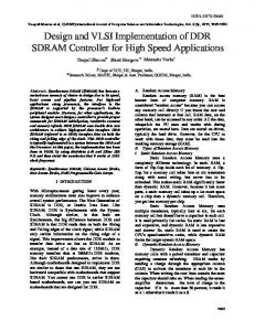
TN-46-08: Initialization Sequence for DDR SDRAM Initializing DDR SDRAM Figure 1:
Initialization Flow Diagram Step 1
VDD and VDDQ Ramp
2
Apply VREF and VTT
3
4
5
CKE must be LVCMOS LOW
Apply stable CLOCKs
Wait at least 200µs
6
Bring CKE HIGH with a NOP command (CKE changes to an SSTL_2 input)
7
PRECHARGE ALL
8
Assert NOP or DESELECT for tRP time
9
Configure extended mode register
10
Assert NOP or DESELECT for tMRD time
11
Configure load mode register and reset DLL
12
Assert NOP or DESELECT for tMRD time
13
PRECHARGE ALL
14
Assert NOP or DESELECT for tRP time
15
Issue AUTO REFRESH command
16
Assert NOP or DESELECT commands for tRFC
17
Issue AUTO REFRESH command
18
Assert NOP or DESELECT for tRFC time
19
Optional LMR command to clear DLL bit
20
Assert NOP or DESELECT for tMRD time
DRAM is ready for any valid command
PDF: 09005aef80ff2dde/Source: 09005aef80eaf953 TN46_08.fm - Rev. C 8/10 EN
3
Micron Technology, Inc., reserves the right to change products or specifications without notice. ©2004 Micron Technology, Inc. All rights reserved.
TN-46-08: Initialization Sequence for DDR SDRAM Configuration of Operating Parameters
Configuration of Operating Parameters As part of the initialization sequence, the device operating parameters must be set. For standard DDR SDRAM this includes two internal registers, the mode register (MR), and the extended mode register (EMR). The LMR command is used to program the mode registers. The LMR command is issued in conjunction with the DRAM bank addresses (BA[1:0]) and selects either the MR or the EMR. The DRAM row addresses (A[13:0]) provide the op-code to be written. The least significant row address corresponds to the least significant bit within the mode registers.
Mode Register The mode register (MR) has seven configurable bits that can be dynamically updated to reflect changing system requirements. They include M[2:0], which are used to set the burst length; M3, which is used to set the burst type; M[6:4], which define the CAS latency; and M8, which is used to perform a DLL reset. All other bits are reserved for future use and must be set to 0. To address the mode register, set BA1 = 0 and BA0 = 0. Figure 2:
Mode Register BA1 BA0 A13 A12 A11 A10 A9 A8 A7 A6 A5 A4 A3 A2 A1 A0
15 14 0 0
13 12 11 10 9 8 Operating Mode
7
6 5 4 3 2 1 0 CAS Latency BT Burst Length
M6 M5 M4
Mode Register (Mx)
M3
Burst Type
0
Sequential
0
0
0
Reserved
1
Interleaved
0
0
1
2
0
1
0
4
CAS Latency
0
1
1
8
M2 M1 M0 Burst Length
0
0
0
Reserved
1
0
0
Reserved
0
0
1
Reserved
1
0
1
Reserved
2
1
1
0
Reserved
1
1
1
Reserved
0
M13 M12 M11 M10 M9 M8 M7
Address Bus
1
0
0
1
1
3 (DDR400 only)
1
0
0
Reserved
1
0
1
Reserved
1
1
0
2.5
1
1
1
Reserved
M[6:0]
Operating Mode
0
0
0
0
0
0
0
Valid
Normal Operation
0
0
0
0
0
1
0
Valid
Normal Operation/Reset DLL
–
–
–
–
–
–
–
–
All other states reserved
Notes: 1. Set BA1 =0 and BA0 = 0 to access the mode register. 2. A13 is only used on the 1Gb device. 3. A12 is only used on 256Mb and larger devices.
PDF: 09005aef80ff2dde/Source: 09005aef80eaf953 TN46_08.fm - Rev. C 8/10 EN
4
Micron Technology, Inc., reserves the right to change products or specifications without notice. ©2004 Micron Technology, Inc. All rights reserved.
TN-46-08: Initialization Sequence for DDR SDRAM Extended Mode Register
Extended Mode Register The extended mode register (EMR) has two configurable bits that usually are not changed after the device has been initialized. Bit E0 is used to enable the device DLL and bit E2 defines the output drive strength. All other bits are reserved for future use and must be set to 0. To point to the EMR, set BA1 = 0 and BA0 = 1. Figure 3:
Extended Mode Register BA1 BA0 A13 A12 A11 A10 A9 A8 A7 A6 A5 A4 A3 A2 A1 A0 Address Bus
15 14 13 12 11 10 9 8 7 6 Operating Mode 0 1
5
4
3
2
1
0
DS DLL
Extended Mode Register (Ex) DLL
0
Enable
1
Disable
E1
Drive Strength
0
Normal
1
Reduced
E[1:0]
Operating Mode
0
0
0
0
0
0 0 0 0
0 0
0
Valid
Reserved
–
–
–
–
–
–
–
–
–
Reserved
E13 E12 E11 E10 E9 E8 E7 E6 E5 E4 E3 E2
Notes: 1. 2. 3. 4.
PDF: 09005aef80ff2dde/Source: 09005aef80eaf953 TN46_08.fm - Rev. C 8/10 EN
E0
– – –
–
Set BA1 = 0 and BA0 = 1 to access the EMR. A13 is only used on the 1Gb device. A12 is only used on 256Mb and larger devices. Reduced drive strength is available on x16 devices only.
5
Micron Technology, Inc., reserves the right to change products or specifications without notice. ©2004 Micron Technology, Inc. All rights reserved.
TN-46-08: Initialization Sequence for DDR SDRAM Summary Figure 4:
Initialization Waveform Sequence (( ))
VDD VDDQ
(( )) tVTD
(( ))
VTT VREF
(( ))
T1
T0 CK#
(( )) (( ))
CK
tCH tIS
CKE
Ta0
tCL
tIH
LVCMOS LOW LEVEL ( (
)) tIS
(( )) (( ))
COMMAND
DM
PRE tCK
DQS DQ
Te0
Tf0
(( )) (( ))
(( )) (( ))
(( )) (( ))
(( )) (( ))
(( )) (( ))
(( )) (( ))
(( )) (( ))
(( )) (( ))
(( )) (( ))
(( )) (( ))
(( )) (( ))
(( )) (( ))
(( )) (( ))
(( )) (( ))
ALL BANKS
tIS
tIH
(( )) (( ))
LMR
(( )) (( ))
LMR
(( )) (( ))
tIS (( )) (( ))
AR
(( )) (( ))
AR
(( )) (( ))
ACT5
(( )) (( ))
(( )) (( ))
(( )) (( ))
(( )) (( ))
(( )) (( ))
(( )) (( ))
(( )) (( ))
RA
(( )) ( ( ))
(( )) (( ))
(( )) (( ))
RA
(( )) (( ))
(( )) (( ))
(( )) (( ))
(( )) (( ))
BA
(( )) (( ))
CODE
(( )) (( ))
(( )) (( ))
CODE
(( )) (( ))
(( )) (( ))
BA0 = L, BA1 = L
tIH
CODE tIS
(( )) (( ))
PRE
tIH
CODE
(( )) (( ))
(( )) (( ))
Bank Address (BA0, BA1)
Td0
(( )) (( ))
tIH
NOP
(( )) (( ))
A10
Tc0
(( )) (( ))
tIS
Addresses
Tb0
(( )) (( ))
tIH
BA0 = H, BA1 = L
ALL BANKS
tIS
tIH
(( ))
High-Z
(( ))
(( ))
(( ))
(( ))
(( ))
(( ))
(( ))
High-Z
(( ))
(( ))
(( ))
(( ))
(( ))
(( ))
T = 200µs tRP
tMRD
Power-up: VDD and CK stable Load Extended Mode Register
tMRD
tRP
tRFC
tRFC5
200 cycles of CK with CKE HIGH are required before any READ command Load Mode Register
DON’T CARE
Summary The proper DRAM initialization sequence must be followed whenever the device is first powered up or anytime there is an interruption in device power. Failure to follow documented steps will jeopardize device functionality. The steps in this technical note provide a general flow for proper initialization; for exact device timing or device voltage levels, refer to the DDR component data sheet(s). For the latest data sheets, refer to Micron’s Web site at www.micron.com/products.
8000 S. Federal Way, P.O. Box 6, Boise, ID 83707-0006, Tel: 208-368-3900 www.micron.com/productsupport Customer Comment Line: 800-932-4992 Micron and the Micron logo are trademarks of Micron Technology, Inc. All other trademarks are the property of their respective owners. This data sheet contains minimum and maximum limits specified over the power supply and temperature range set forth herein. Although considered final, these specifications are subject to change, as further product development and data characterization sometimes occur.
PDF: 09005aef80ff2dde/Source: 09005aef80eaf953 TN46_08.fm - Rev. C 8/10 EN
6
Micron Technology, Inc., reserves the right to change products or specifications without notice. ©2004 Micron Technology, Inc. All rights reserved.
TN-46-08: Initialization Sequence for DDR SDRAM Revision History
Revision History Rev. C . . . . . . . . . . . . . . . . . . . . . . . . . . . . . . . . . . . . . . . . . . . . . . . . . . . . . . . . . . . . . . . . . . . . . . . . . . . . . . . . . . . . . . . . . . . . . . . 8/10 • Initializing DDR SDRAM: Updated description. • Figure 1: Initialization Flow Diagram: Updated figure. • Updated template and formats. • Minor grammatical corrections. Rev. B . . . . . . . . . . . . . . . . . . . . . . . . . . . . . . . . . . . . . . . . . . . . . . . . . . . . . . . . . . . . . . . . . . . . . . . . . . . . . . . . . . . . . . . . . . . . . . 10/05 • Updated template. • Corrected step 9. Rev. A . . . . . . . . . . . . . . . . . . . . . . . . . . . . . . . . . . . . . . . . . . . . . . . . . . . . . . . . . . . . . . . . . . . . . . . . . . . . . . . . . . . . . . . . . . . . . . . 1/04 • Initial release.
PDF: 09005aef80ff2dde/Source: 09005aef80eaf953 TN46_08.fm - Rev. C 8/10 EN
7
Micron Technology, Inc., reserves the right to change products or specifications without notice. ©2004 Micron Technology, Inc. All rights reserved.