design flow starts with modeling the design using Verilog HDL code, simulated by .... The u_data_valid signal is asserted when read data is valid on u_data_o.
P.Anup et al, / (IJCSIT) International Journal of Computer Science and Information Technologies, Vol. 3 (3) , 2012,4270 - 4274
A Low Power DDR SDRAM Controller Design P.Anup , R.Ramana Reddy Dept. of ECE, MVGR College of Engineering, Andhra Pradesh, India Abstract— This paper work leads to a working implementation of a Low Power DDR SDRAM Controller that is meant to be used as a reference for future implementations. . The DDR SDRAM is an enhancement to the traditional Synchronous DRAM. It supports data transfers on both edges of each clock cycle, effectively doubling the data throughput of the memory device. In this project Low Power Techniques are proposed for DDR SDRAM Controller and which is implemented with 180nm CMOS Technology by using Cadence tools. The proposed controller performance is evaluated at a clock rate of 133MHz, 64-bit data changing at both clock edges with a burst length of 4 and with read CAS (Column Address strobe) latency 2. In order to implement proposed DDR SDRAM Memory Controller, the hardware design flow starts with modeling the design using Verilog HDL code, simulated by using Cadence NC Simulator, synthesized by making use of RTL Compiler. Keywords— Column address strobe, Dual data rate (DDR), Synchronous dynamic RAM.
I. INTRODUCTION The DDR SDRAM is an enhancement to the traditional Synchronous DRAM. It supports data transfers on both edges of each clock cycle, effectively doubling the data throughput of the memory device. The DDR SDRAM operates with a differential clock: CLK and CLK#. Commands (address and control signals) are registered at every CLK positive edge. Input data is registered on both edges of the DQS (data strobe), and output data is referenced to both edges of DQS, as well as to both edges of CLK. A bidirectional data strobe signal is transmitted by the DDR SDRAM during reads and by the memory controller during writes. Read & writes accesses to the DDR SDRAM are burst oriented. Accesses begin with the registration of an ACTIVE command, which is then followed by a READ or WRITE command. A DDR SDRAM is divided into four banks where each bank consists of a number of rows. A row is then divided into columns which each contains 64 bits of data. The number of rows and columns are dependent on the size of the DDR SDRAM and the internal organization. The organization with four banks makes it possible to issue one command to every bank. It is not possible though to make more than one read or write operation at a single time since the data bus only can handle data for one operation. This paper is organized as follows. In Section II, Block diagram and architecture for the proposed design will be described. Timing diagram will be described in Section III. In Section IV, low power technique will be explained. Finally, Results and conclusion will be given in Section V and Section VI respectively. II. BLOCK DIAGRAM AND ARCHITECTURE The DDR controller module contains the DDR SDRAM controller, including I/Os to interface as shown in Fig. 1.
Fig. 1 Block diagram
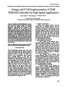
The architecture of ddr sdram is shown in Fig. 2. DDR Controller consists of four functional block diagram: 1) Address Latch 2) Controller 3) Data Path 4) Counter
Fig. 2 Architecture of DDR SDRAM
A. Address Latch The address latch module gets its control signals from the controller, and generates row, column, and bank addresses for the DDR SDRAM. The address latch also generates burst_max, cas_lat_max values for the burst counter (brst_cntr), and cas-latency counter (cslt_cntr). The controller generates address and control lines on the negative edge of clk to guarantee the hold time on the DDR 4270
P.Anup et al, / (IJCSIT) International Journal of Computer Science and Information Technologies, Vol. 3 (3) , 2012,4270 - 4274
SDRAM. The physical pin diagram of address latch is shown in Fig.3
D. Controller Controller consists of a state machine which perform DDR SDRAM read and write accesses based on user interface request. The controller consists of a high performance timing and control state machine that observes all timing requirements and issues the commands to the memory devices at the earliest time possible. The physical pin diagram of controller is shown in fig.5.
Fig.3 pin diagram of address path
SDRAM device has only 12 physical address pins, whereas the address bus provides 22 address pins. What makes it possible to interface between user and DDR SDRAM when there is an uneven number of pins is through an internal address multiplexing via the SDRAM controller in single mode. When performing load mode register command MRS (mode register set) address is used to set operating condition for DDR SDRAM B. Data Path Data Path module transmits data to the memories. Major functions include storing the write data and calculate value for the read data path. Data between the user interface and the DDR SDRAM is transferred at both the rising edge and falling edge of the clock input. This creates very tight timing requirement for generating write data and sampling read data. For read access, data is sampled by the data path and the double data rate. The physical pin diagram of data path is shown in Fig. 4.
Fig.4 pin diagram of Datapath
The DDR Data Path block contains the circuitry to manage data flow to and from the DDR SDRAM. When transmitting data to the DDR SDRAM device, the n-bit data is split into two (n/2)-bit data. The MSB (n/2) data bits are transferred to Dq when clock is 0; the LSB (n/2) data bits are transferred to Dq when clock is 1. Since the Dqs (data strobe) signal must be center-aligned in respect to the data, the clock signal is delayed by δt1 and transmitted to Dqs. C. Counter Burst Counter: Burst count value counter when there are consecutive READ or WRITE While doing consecutive READ or WRITE, the Burst_count value determines when the next READ or WRITE command should be issued. The DDR controller consists of a high performance memory controller for system requiring access to external devices with lowest latency and highest throughput.
Fig. 5 Pin diagram of controller
The controller accepts and decodes user interface commands and generates read, write, refresh commands. The controller also generates signals for other modules. The memory is initialized and powered up using a defined process. The controller state machine handles the initialization process upon power up. E. Controller state diagram The Controller is initially in the IDLE state. Following the NOP command, a PRECHARGE ALL command should be applied. The PRECHARGE command is used to deactivate the open row in a particular bank or the open row in all banks. Once a bank has been precharged, it is in the idle state and must be activated prior to any READ or WRITE commands being issued to that bank. Next a LOAD MODE REGISTER command should be issued for the extended mode register (BA1 LOW and BA0 HIGH) to enable the DLL, followed by another LOAD MODE REGISTER command to the mode register (BA0/BA1 both LOW) to reset the DLL and to program the operating parameters. Two-hundred clock cycles are required between the DLL reset and any READ command. A PRECHARGE ALL command should then be applied, placing the device in the all banks idle state. bank. A PRECHARGE command will be treated as a NOP if there is no open row in that bank (idle state), or if the previously open row is already in the process of precharging. Once in the idle state, two AUTO REFRESH cycles must be performed (tRFC must be satisfied.) The next state of the controller could be PRECHARGE, LOAD_MR, REFRESH, or ACT, depending on the required command. The dashed lines in the state machine diagram show an automatic sequence. Before any READ or WRITE commands can be issued to a bank within the DDR SDRAM, a row in that bank must be “opened.” This is accomplished via the ACTIVE command, which selects both the bank and the row to be activated. After a row is opened with an ACTIVE command, a READ or WRITE 4271
P.Anup et al, / (IJCSIT) International Journal of Computer Science and Information Technologies, Vol. 3 (3) , 2012,4270 - 4274
command may be issued to that row, subject to the tRCD specification. tRCD (MIN) should be divided by the clock period and rounded up to the next whole number to determine the earliest clock edge after the ACTIVE command on which a READ or WRITE command can been entered.The figure 6 expalins the state diagram of the SDRAM CONTROLLER
command and the SDRAM address are placed on u_cmd and u_addr. At T2, the controller goes from IDLE to ACT state. At T3, the controller issues an ACT command and row address to the DDR SDRAM. After TRCD delay (three clk cycles), the controller issues a READA command and column address. After CAS latency (two clock cycles), the DDR SDRAM presents the data and data strobe at every clock edge until the burst is completed. The controller receives the data and assembles it back into 128-bit words. The u_data_valid signal is asserted when read data is valid on u_data_o.
Fig. 6 controller state diagram
III. TIMING DIAGRAM A. Write cycle Fig.7 shows the timing diagram for writing a burst of eight data words to the DDR SDRAM. The first four signals are inputs to the DDR controller. At T1, the write command, DDR SDRAM address, and the first 128-bit data are placed on u_cmd, u_addr, and u_data_i respectively. The fifth waveform shows state of the controller. The controller goes from IDLE into ACT state at T2. The last four waveforms show the signal interfaces to the DDR SDRAM. At T3, the controller issues the ACT command and the row address to the DDR SDRAM. After TRCD delay (three clock cycles), the controller issues the WRITEA command and column address. The signals ddr_dq and ddr_dqs, are then issued at a double data rate.
Fig.7 write cycle timing diagram
B. Read cycle Fig. 8 shows the timing diagram for reading a burst of eight data words from the DDR SDRAM. At T1, the read
Fig. 8: read cycle timing diagrams
IV. LOW POWER TECHNIQUE With the advent of portable and high-density microelectronic devices, the power dissipation of very large scale integrated (VLSI) circuits is becoming a critical concerned. The continuing decrease in feature size and the corresponding increase in chip density and operating frequency have made power consumption a major concern in VLSI design Power dissipation is an important consideration in the design of CMOS logic circuits. Although power consumption is important for modern VLSI design, operation speed and occupied area are still the main requirements of the VLSI design .Two different low power techniques used in this paper are clock gating and multi threshold voltage technique. A. Clock gating Clock gating is the most common way to reduce dynamic power.Clock gating selectively disables the clock to eliminate unnecessary switching activity which significantly reduces the dynamic power.Clock gating saves power by adding more logic to the circuit by disabling the clock ,so that flip flops do not have to switch states. B. Multi threshold technique Multi threshold voltage CMOS (MTCMOS) technology is a good solution which provides a high performance and low-power design without any area overhead This low power technique is used to reduce the leakage power in the device. The multi-vt technique can reduce the leakage power by using replacing std Vth cells with high Vth cell. For non critical path high Vth cells (low leakage and slow timing performance) are used. For critical path std Vth cells (high leakage power and high timing performance) are used. 4272
P.Anup et al, / (IJCSIT) International Journal of Computer Science and Information Technologies, Vol. 3 (3) , 2012,4270 - 4274 Table 1.Power consumption comparison results
Leakage power (nW)
Dynamic power (nW)
Total power (nW)
No.clock gating cells
Percentage Reduction in Total power
Without low-power technique
5873.089
240130.819
2436003.908
4
--
Clock gating technique
5870.089
2379979.625
2385847.256
4
2.05%
Multi Vt Technique
1075.713
2400130.80
2401206.513
4
1.42%
Clock gating + multi Vt technique
975.713
2361872.261
2362847.974
4
3.003%
V. RESULTS The DDR SDRAM is implemented in the 180nm technology and low power techniques are applied to it. The Table1 above shows the comparisons of the power consumed without applying low power technique and with applying low power techniques. The graph in Fig.9 shows the reduction in leakage power when the different low power techniques are applied.
Fig.11 Top view schematic of ddr sdram controller
The following figure are the simulation results which are obtained using cadence NCsim tool.
Fig.9 leakage power reduction graph
The graph in fig. 10 shows the reduction in dynamic power and leakage power when the low power techniques are applied.
Fig.12 simulation waveform for Read cycle
Fig.10 Reduction in dynamic power and total power
The Following figure11 shows schematic top view of DDRSDRAM controller.
Fig. 13 Simulation waveform for write cycle
4273
P.Anup et al, / (IJCSIT) International Journal of Computer Science and Information Technologies, Vol. 3 (3) , 2012,4270 - 4274
VI. CONCLUSION The proposed ddr controller is implemented with 180nm CMOS Technology, using Cadence tools. The proposed design is modeled in Verilog HDL and then simulated using ncsim, synthesized by making use of RTL Compiler and physical implementation by using Encounter. The performance of the design is evaluated at a frequency of 133MHz, 64 bit data is transferred on both the edges of clock with burst length 4 and CAS latency 2.Low power techniques are applied and their reports are studied and compared. The total power obtained using the integration of multi Vt and Clock gating is less than the power obtained using other techniques.
REFERENCES
[1] [2] [3] [4] [5] [6] [7]
J.Bhaskar “ A verilog HDL primer – 2nd Edition.” John Wakerly “Digital systems design – 8th Edition.” Jedec solid state technology association -Double data rate SDRAM specification Neil H.weste “Principles of CMOS VLSI design- 2nd edition.” RTL encounter user guide and Cadence user guide. Samir palnitkar “ Verilog HDL A guide to digital design and synthesis – 2nd Edition.” Xilinx Inc., XAPP179, using select IO interfaces, application note
4274