Quasi 2D grows at low temperature ... wurzite-type with perovskite-type structures and exploiting the large dielectric constant of SrTiO3 we realized field effect.
Transport properties of non magnetic and magnetic ZnO thin films under Field Effect
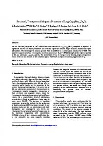
Transfer characteristics & field effect mobility 10
-7
-8
10
-9
Deposition of high crystalline quality Al and Co doped ZnO films grown by pulsed laser deposition on 110 face of strontium titanate single crystals. • Transparent semiconductor • High mobility • Wide-band gap • Doped with magnetic ions (Co, Mn…): dilute magnetic semiconductors
Perovskite oxides
Drain
-10
-20
I Source
Drain
��
gate
Gate
E
Source
Active channel
Drain
Source
VG (V) +200 +100 0 -100 -200
-1
-10
10
-11
10
Vds= 0.3 V 20
5
0
1
2
3
VSD [V] VG=5 V 4V
6
3V
4
2V 1V
2
5 0 25
10 15 Vg [V]
0 0
2
4
6
VSD [V]
10
9
10
8
10
7
10
6
0
10
20
30
40
50
60
70
80
90
100
T [K] εr
Thermal activated behaviour MIT driven er of the STO substrate Competition between T and V dependences of εr
10
T [K] VG [V]
C ExpDec1 fit of Data1_C
0.15
-4
0
50
100
150
200
T [K] 10
19
0.10
ΔE [eV]
10
19
Mobility and threshold voltage as a function of the Temperature
10
ΔE ∝ e
−n
cost.
0.05
18
10 10
20
18
3
n (e /cm )
3
16
0 -2
14 -4
12 2
17
-
-
10
16
10
T [K] 5 10 15 20 25 30 35 40 45 50 55 60 65 70 75 80 85 90 95 100
2
18
Meas. Calc. T(K) 2.5 5 10 50 100
17
10
VG [V] 50 100 150 200
Vs [V]
570 °C
μ [cm /Vs]
650 °C
0
-1
8
2
10
-2
n [e /cm ]
730 °C
15
10
Differentially pumped RHEED gun Computer controlled multitarget carousel for multilayer deposition Deposition temperature from 550 to 800 °C Oxygen deposition pressure from 10-5 to 2 10-1 mbar ZnO stoichiometric target: doping control by oxygen deficiency ZnO:Al 0.05%-0.5% : more controlled doping 1%-10% Co codoped targets for DMS samples
800 °C
20
-9
SrTiO3 110 permittivity vs VG and T
-3
• • • • • • •
25
-8
-2
10
30
0
10
ρ [Ωcm]
Pulsed laser deposition on STO 110 Substrate:
-3
35
-7
Resistivity vs temperature for different applied Gate Voltages.
• High Tc superconductivity • Ferroelectricity • Ferromagnetism, Colossal Magnetoresistance • Semiconductors, Insulators
10
77K
10
ZnO:Al 0.2% at. 10
0 VG [V]
0
10
Field Effect (FE) experiment, allowing to change the carrier concentration of the film by more then 4 order of magnitude (from ≈1015 to ≈1020 e-/cm3, estimated by Hall effect measurements under FE), were employed to deeply investigate transport mechanisms. In particular we observed a crossover of low temperature magnetoresistance from a negative behavior in accumulation state to a positive one in depletion state. The measure of the activation energy as a function of the Gate potential allowed us to get information on the density of states
Many physical properties depending on cations
A: Alkaline Earth B: Transition Metal (Pseudo)cubic Lattice Parameter (3.9 ± 0.1)Å
-10
0.25 0.5 1 2 3
-1.5
In the ISD-VSD characteristic curves a typical MOSFET-like pinch off behavior is observed: the current tends to saturate for high source-drain voltages. The complete saturation regime is however not reached probably because channel thickness larger than the estimated Debye length (below 10 nm for a carrier density of 1017 e/cm3). Gate leakage current detectable only for voltages higher than 30 V
Gate
ZnO STO single X-tal Ag (ZnO)
-6
0.0 -0.5 -1.0
2
ISD [μA]
ISD [A]
gates
4
10
R [Ω]
Hexagonal Lattice parameters a=3.24 Å, c=5.19 Å
Side Gate Geometry
6
Vg [V] -1 -0.5 -0.25 0
0.5
2
10
10
Field effect experiments:
1.0
8
10
The integration of ZnO based high mobility transparent semiconductors with perovskites that exhibit a wide spectrum of physical properties (superconductivity, ferroelectricity, ferromagnetism, etc.) may lead to a wide variety of new electronic/optoelectronic devices; recently we reported about the realization of epitaxial ZnO/SrTiO3 heterostuctures and about their application in the fabrication of field effect transistors transparent at visible wavelength
1.5
10
μFE [cm /Vs]
ISD [A]
CNR-INFM Lamia, Corso Perrone 24, 16152 Genova, Italy Dipartimento di Fisica, Università di Genova, Via Dodecaneso 33, 16146 Genova, Italy
Back Gate Geometry
2.0
300K
E. Bellingeri, I. Pallecchi, L. Pellegrino, A.Caviglia, G. Canu, A. Gerbi, M. Vignolo, A.S. Siri, D. Marré
Characteristic curves 77 K
12
ISD [μA]
-6
μEF [cm /Vs]
10
15
10
0
20
40
60
80
100
T [K]
10 8 6
10
16
14
0
50
100
150
10
200
-200
-150
-100
-50
T [K]
0
50
100
150
4
200
2
Vg (V)
Calculated induced carrier from device-capacitance vs T
Hall effect measured and calculated induced carrier vs Vg: agreement in accumulation regime.
0 -6
-3
0
3
6
0.00 -2
0
2
4
6
8
10
Vg [V]
Estimation of the density of state (impurity band) D(E)∝1/(E-Ec)
9
Vg [V]
Magnetoresistance at different temperatures and applied Gate voltages: 2
4
6
8
10
Zn0.95Co0.05O:Al 0.2% at.
-0.010 0.00
-0.03 0.00
31.0
30.5
30.5
62.5
63.0
63.5
30.0 62.0
62.5
63.0
63.5
2θ
Δρ/ρ0
Low crystallinity ZnO buffer layer at low temperature
2
ZnO 101
-3
n [10 e /cm ]
Counts [A.U.]
8
16 -
180
240
300
360
φ [Deg]
• • • • •
2
aB 2 1 + dB 2
Δρ s − d
⎛ σ μ + σ 2 μ2 ⎞ d = ⎜⎜ 1 1 ⎟⎟ ⎝ σ1 + σ 2 ⎠
ρ0
4
6
8
= − g 2 (1 + h 2 B 2 )
66.00 77.00
110.0
70.00
112.0
0 700
600
500
400
300
Wavelength [nm]
NO absorption on the visible part
-5
1.4x10
-5
1.2x10
-5
1.0x10
-5
1 00
1 50
200
2 50
3 00
35 0
126.0 140.0
]
2
4
6
8
0
10
50
1 00
1 50
200
25 0
3 00
3 50
T (K )
X A xis Title
2
1.6
T=5K
1.3
Small ferromagnetic signal at RT More pronounced at low temp.
0.8 0.5 0.3 0.0 -0.3 -0.5
0.05
0.10
0.15
0.20
0.25
0.30
0.35
0.40
-1.0
10
14
15
16
10
17
10
18
10
19
10
10
0.45
0.50
0.10 0.08 0.06 0.04 0.02 0.00 -0.02 -0.04 0.8
3
4
5.0x10
2.0
0.0
0.2
0.4
0.6
0.8
1.0
50 10 0 -5 -10
150 50 10 0 -5
0.4 0.2 0.0 -0.2
h
g
1.0
0.10
0.5 0.05
150 50 5 0 -1 -2.5 -7.5
1.0 0.5 0.0
0.00
0.0 14
15
10
16
17
10
10 -
3
n (e /cm )
18
10
19
10
14
10
10
15
16
17
10
10 -
18
10
19
10
3
n (e /cm )
Optical properties similar to bulk
CONCLUSION We deposited epitaxial zinc oxide thin films on (110) strontium titanate substrates, proving the possibility to integrate wurzite-type with perovskite-type structures and exploiting the large dielectric constant of SrTiO3 we realized field effect transistor. These devices were employed to study the intrinsic properties of magnetic and non magnetic zinc oxide thank to the capability of change the carrier density by more then 5 order of magnitude.
2.5 2.0 1.5 1.0 0.5 0.0 -0.5 3
150 50 10 10 5 0 -1 -2.5 -5
5K
150 100 50 10 0 -2 -5 -6
2.5 K
2 1 0 0
-1
This MR behavior seem due to the influence of magnetic polarons and of the exchange-induce spin splitting on the quantum correction to the conductivity of disorder magnetic materials.
Sawiki et al PRL 56 508 (1986) Andrearczyk et al PRB 72 121309 (2005)
10K
1.5
0.15
10
0.0 2.6 2.8 3.0 3.2 3.4 3.6 3.8 4.0 Photon Energy (eV)
-0.2
20 K
0.6
Δρ/ρ0
5
1.0x10
-0.4
50 K
1.5
650 °C 730 °C 800 °C
-0.6
μ0H (T)
0.20
5
-0.8
Field effect experiment in order to correlate magnetic properties and carrier density: Magnetoresistance
Δρ/ρ0
10
-5
1.6x10
98.00
Δρ/ρ0
20
1.8x10
50
84.00
4
The agreement of the least-squares fits to the data is excellent for all the Gate voltages and temperatures. Plots of the fitting parameters versus the measured carrier concentration shows a very systematic concentration and temperature dependence
T [K] 2.5 5 10 50 100
a 30
Absorption Coefficient (1/cm)
Transmittance [%]
+ ZnO Film
40
2.0x10
-5
-1.3
0.8
0.0 0.00
0.25
50
-5
T (K )
6
-1
2.5x10
5
-5
2.2x10
0
8
4.0
1.5x10
1.6x10
10
14.00
Photon energy (eV)
STO
8
0
1/T [K ]
Optical properties:
60
6
-0.8
0.2
10
-
70
4
10
n [e /cm ]
5
The FC and ZFC separation temperature is related to the order of the crystal structure
X Ax is Title
VG [V] -200 -100 -50 0 50 100 150 200
0.4
-2
-5
2.0x10
3 50
99.00
2
⎡ (2 Jρ F ) ⎤ ⎛ g 0 μ ⎞ h 2 = ⎢1 + 4 S 2π 2 ⎟ ⎥ ⋅⎜ g0 ⎣ ⎦ ⎝ αKT ⎠
0.6
300
10
80
3 00
88.00
6
2
4
1.0
10
470 nm thick T [K]
-4
90
25 0
-1.6
10
3.6
-5
200
55.00
1.1
2
•Exponential increase decreasing the temperature (up to 400 cm2/Vs @ 10K)
3.2
-5
1.8x10
1 50
-1.1
0
•Mobility values up to 80 cm2/Vs at RT
2.8
2.0x10
1 00
44.00
1.4
-3
2.4
-5
50
T (K )
8
1.6
10
2.0
2.2x10
0
33.00
F.Reuss et al APL 87 112104 (2005) Khosla and Fisher PRB 2 4084 (1970)
μ0H [T]
200
-5
22.00
2
2.5 K
10
100
2.4x10
10
11.00
1.2
8
8
10
2
[
0.1
Resistance
6
0
σ σ (μ − μ ) 2 a = 1 2 1 22 (σ 1 + σ 2 )
g 2 = A1 Jρ F S ( S + 1)+ < M 2 >
0.0
6 001 growth 0 Excellent epitaxial growth Single in plane orientation Quasi 2D grows at low temperature Low roughness
100
4
X A xis Title
Negative MR terms arising from third order expansion of the s-d exchange Hamiltonian
0.2
2
R [kΩ]
120
Carrier density
4
12
5K
0.3
6
2
-0.05
100
45.00
4
56.00
-0.10
200
14 60
Δρ/ρ0
300
0
STO 100
Hall mobility
-5
Deposition Temperature
40.50
42.00
0.00
Δρ/ρ0
μ [cm /Vs]
400
36.00
6
28.00
0.05
High crystallinity ZnO active layer at high temperature
Flat and high mobility samples
ρ0
-0.10 0.10
Two steps deposition:
3.5x10
ZFC FC
31.50
Δρ/ρ0
Like on Al2O3 substrate
=
-5
27.00
10 K ΔρCO
-5
4.0x10
22.50
4
-0.05
-1
2θ
h [T ]
30.0 62.0
Temperature and thickness improove crystalline quality but increase roughess
-5
4.5x10
18.00
Classical positive magnetoresistance in a two band model arising from the action of the Lorentz force on the mobile carriers. For carriers in closed orbits the term is of the form:
ω
ω 31.0
0
50 K -0.02
5.0x10
13.50
m (emu)
550 °C
31.5
9.000
Δρ/ρ0
32.0
31.5
4.500
8
m (μB/Co)
32.5
750 °C
32.0
Δρ/ρ0
32.5
-0.01
Field Cooled and Zero Field Cooled magnetization 0
10
Y Axis Title
Rough 0.43 nm r.m.s
Rough 2.9 nm r.m.s
Correlation of structural and magnetic properties HRXRD Reciprocal space map
m (emu)
100 K
Y Axis Title
-0.005
Y Axis Title
Δρ/ρ0
Meas. Fit VG [V] 200 150 100 50 0 -50 -100 -200
m (emu)
0 0.000
-2
-3
-4
-5
μ0H [T]
-6
-7
-8
-9
-10