Ultra-low noise field-effect transistor from multilayer graphene Atindra Nath Pal∗ and Arindam Ghosh
arXiv:0905.4485v1 [cond-mat.mes-hall] 27 May 2009
Department of Physics, Indian Institute of Science, Bangalore 560 012, India We present low-frequency electrical resistance fluctuations, or noise, in graphene-based field-effect devices with varying number of layers. In single-layer devices the noise magnitude decreases with increasing carrier density, which behaved oppositely in the devices with two or larger number of layers accompanied by a suppression in noise magnitude by more than two orders in the latter case. This behavior can be explained from the influence of external electric field on graphene band structure, and provides a simple transport-based route to isolate single-layer graphene devices from those with multiple layers.
Graphene, single atomic layer of hexagonal carbon atoms, has drawn a lot of interest because of its unusual electronic properties1 . In particular, extensive research on single and bi-layer graphene has led to significant improvement in both material properties, as well as fundamental understanding, for nanoelectronic applications2,3,4,5,6 . Carrier mobilities as high as 1 × 104 cm2 V−1 S−1 are now obtained on SiO2 substrate, which is considerably enhanced (∼ 2 × 105 cm2 V−1 S−1 ) in suspended graphene7 . Recently, bilayer graphene8,9,10 has also emerged as a promising material in nanoelectronics in which a tunable band gap can be induced by the application of perpendicular electric field6,11 or chemical doping4,5 . In contrast however, the behavior of few-layer graphene devices with three or more atomics layers remains relatively unexplored. The significance of this issue is immense in view of the difficulty in large scale production of single and bilayer graphene devices, with several chemical methods12 , such as those involving reduction of graphite oxide13 , routinely producing high-quality multilayers of graphene. Uncertainties exist at the theoretical front too, where the band structure calculations in trilayer graphene within the tight-binding framework in the presence of an external electric field yielded both opening of a gap14 and semi-metallic behavior15 . Although recent experiments16 with double-gated trilayer devices support the latter, conventional time-averaged characterization schemes, such evolution of carrier mobility with increasing layer number17 , seems to be inadequate in understanding the overall behavior of gated multilayer graphene. Being directly sensitive to the ability of an electronic device to screen external potential fluctuations, the lowfrequency noise in electrical transport has recently been shown to reflect the low-energy band structure in single and bilayer graphene devices11,18 . Although the noise in both cases was found to originate from the disorder present in the SiO2 substrate, primarily in the form of fluctuating charge traps, the dependence of noise magnitude on the gate electric field was found to be opposite for single and bilayer graphene, and was attributed to a
∗ electronic
mail:
[email protected]
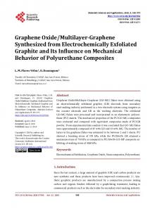
(a)
(b)
FIG. 1: Color Online. (a) Raman spectra for SLG, BLG, FLG and MLG showing the characteristic G and 2D peaks. (b) Gate voltage characteristics of graphene devices: for comparison, the ratio of resistivity (ρ) and the resistivity at the CNP (ρD ) are plotted as a function of (Vbg − VD ) at T = 100 K. The inset shows the optical micrograph and outline of a typical graphene device. The scale bar is 5µm.
field-induced gap formation in the latter. In the context of device application, however, both systems exhibited large noise magnitude (γH ∼ 1 × 10⁻³ , where γH is the phenomenological Hooge parameter)11,18 similar to carbon nanotube FET devices19,20 , although some experiments21 report lower values of γH ∼ 1 × 10⁻⁴ . As an emerging new material, an investigation of noise performance of multilayer graphene devices is thus necessary for both application and fundamental perspectives. Here, we present a systematic study of low-frequency noise measurements in four categories of graphene devices: single layer graphene (SLG), bilayer graphene (BLG), few-layer graphene (FLG) with 3 − 5 atomic lay-
2
(b)
BLG
5 1000
2
2 500
0
60
1 -60 60
90
(d)
4 300 3
0
20
Back Gate Voltage (V)
20
40
60
115
MLG
40
-10
3 110
2
Resistance (Ω)
5
-20
0
6
NR = δR2/R2 (10-10)
Resistance (Ω)
FLG 400
-40
-20 20
Back gate Voltage (V)
(c)
-60
-40 40
2
105
100
2
30
Back Gate Voltage (V)
NR = δR /R (10 )
0
-8 8
3
1000
2
10
2
2000
2
-8
15
Resis stance (Ω)
SLG
NR = δR /R (10 )
Re esistance (Ω)
3000
NR = δR /R (10 )
20
(a)
1
-40
-20
0
20
Back Gate Voltage (V)
FIG. 2: Color Online. The resistance and the normalized noise power spectral density (NR ) as functions of back gate voltages are shown for: (a) SLG (b) BLG (c) FLG and (d) MLG devices at T = 100 K. The thick solid lines are guide to the eye. The insets in each figure correspond to the bandstructure at particular voltages for corresponding graphene flake.
ers, and many-layer graphene (MLG) with greater than 5 layers in the device. The noise magnitude at a given carrier density (n) was observed to be two orders of magnitude lower in the FLG and MLG devices in comparison to that in SLG and BLG. Also, noise magnitude in SLG decreases with increasing n, while BLG, FLG and MLG devices show an increase in noise on both side of the charge neutrality point (CNP), making noise in our case an excellent transport-based probe to identify single layer graphene devices from the multilayered ones. Graphene flakes were prepared on 300 nm SiO2 on n++ doped silicon substrate (the backgate) by micromechanical exfoliation of HOPG. All flakes were characterized by Raman spectroscopy, and subsequent atomic force microscopy indicated the FLG and MLG devices in the present case to consist of 3-4 and ≈ 14 layers, respectively. 40 nm gold contacts were defined using standard electron beam lithography technique. Optical micrograph of a typical device is shown in the inset of Fig. 1b. All devices were prepared on identically processed substrate from the same Si/SiO2 wafer to keep the disorder level comparable. Fig. 1a shows the characteristic Raman spectra for different graphene flakes where the intensity ratio of the G peak to the 2D peak can be seen to increase with increasing layer number22 . Fig. 1b shows the gate voltage characteristics of the devices. In all the cases, CNP was shifted to a finite gate voltage due to the intrinsic doping (see Fig. 2 also). Hence in order to compare the influence of gating we have plotted the ratio of resistivity to that at the CNP as a function of (Vbg − VD ), where VD is the back gate voltage at CNP. Fig. 1b clearly demonstrates the ambipolar tran-
sistor action in all devices, although the effect of gating decreases with increasing layer numbers23,24 . Mobility of SLG, BLG, FLG and MLG devices were calculated to be 1100, 1160, 2450 and 1200 cm2 V−1 S−1 respectively. Noise in the graphene devices were measured in lowfrequency ac four-probe method. A carrier frequency of 777 Hz was used to allow measurement bandwidth of 256 Hz. Typical noise measurement involves digitization of the time-dependent output of the lockin amplifier, followed by multistage decimation of the signal to eliminate effects of higher harmonic of the power line or other unwanted frequencies, and finally estimation of the power spectral density. (See Ref [25] for details.) The excitation was below 50 µA to avoid heating and other non-linearities, and verified by quadratic excitation dependence of voltage/current noise at a fixed resistance R. The background noise was measured simultaneously, and subtracted from the total noise. In all devices the normalized resistance noise power spectral density behaved as, SR (f ) = γH R2 /nAG f α , where AG is the area of the flake between the voltage probes (not shown). The noise power spectral density was found to be proportional to 1/f α , with α ranging from 0.8 − 1.2 (see Ref [11]). Here, instead of focusing on γH or noise magnitude at a specific frequency, we compute and analyze the total variance of resistance R fluctuations NR = hδR2 i/R2 = (1/R2 ) SR (f )df , where the integration is carried out numerically over the experimental bandwidth. Fig. 2a-d shows the variation of NR and the corresponding average resistance as a function of back gate voltage (Vbg ) for SLG, BLG, FLG and MLG devices respectively. In case of SLG, noise decreases with increasing n on either side of the CNP (the Dirac point), which can be understood by better screening of potential fluctuations. But in all other cases, noise magnitude behaves oppositely. In case of BLG, one can break the interlayer symmetry by applying a perpendicular electric field across the flake, resulting in a gap between the conduction and valence band4,8,9 . Screening of the external potential fluctuations weakens with increasing bandgap, leading to enhancement of noise at higher gate field11,18 . Moreover, the rate of change of noise in SLG as a function of gate voltage was found to be larger than the other devices, indicating its different microscopic origin. The qualitative similarity in the gate voltage dependence of noise in FLG and MLG to that of BLG naturally indicates a common underlying physical mechanism. The band structure of gated three and four layer graphene has been recently carried out within the tight binding scheme with Slonczewski-Wiess-McClure coupling parameters, taking screening into account in a self-consistent manner14,15,26 . In the presence of a layer-symmetry breaking electric field on trilayers, however, the theoretical calculations differ, although recent experimental results16 suggest an enhancement in the overlap of conduction and valence bands with increasing field. In our devices, however, the increase in noise in FLG and MLG with increasing |n| suggests a reduction in the density-of-state (DOS)
3 hence can be used for FLG nanoribons. 0.01
12
2
n = 2.4× 10 /cm
SLG FLG MLG
γΗ
1E-3
1E-4
1E-5
0
100
200
300
Temperature (K)
FIG. 3: Color Online. (a) Temperature dependence of Hooge parameter for SLG, FLG and MLG devices. (b) Hooge parameter as a function of graphene thickness for three different temperatures, 20 K, 100 K and 296 K, far from the CNP (n = 2.4 × 10¹² /cm2 ).
at low energies, hence a field-induced pulling apart of the bands, which may eventually lead to a gap at the Fermi energy14 . (Note that in our case the thickness of the FLG is determined by atomic force microscopy, and hence uncertain between three or four layers) The reason behind this difference is not clear, though a difference in stacking sequence in the FLG/MLG devices may be envisaged. Indeed, it has been shown23,26,27 that while ABAB... Bernal stacking remains semi-metallic under external field, a rhombohedral type (ABCA...) stacking displays opening of a gap under transverse electric field. Nevertheless, along with time-averaged resistivity, noise seems to be a robust probe in this context, which can differentiate between such stacking modes in multilayer graphene on thermodynamic (screening) grounds. Moreover, it is also important to note that, in these cases, noise measurements form an excellent transport based technique, that immediately separates the SLG device from thicker ones without the need to go to the quantum Hall regime. It also does not require Hall probes and
1 2 3
4 5 6 7 8
9 10
11
K. S. Novoselov et al., Science 306, 666 (2004). K. S. Novoselov et al., Nature 438, 197 (2005). A. K. geim and K. S. Novoselov, Nature Mater 6, 183 (2007). E. V. Castro et al., Phys. Rev. Lett. 99, 216802 (2007). T. Ohta et al., Science 313, 951 (2006). J. B. Oostinga et al., Nature Mater. 7, 151 (2008). K. I. Bolotin et al., Solid State Commun. 146, 351 (2008). E. McCann and V. I. Falko, Phys. Rev. Lett. 96, 086805 (2006). E. McCann, Phys. Rev. B 74, 161403(R) (2006). E. V. Castro et al., e-print arXiv:condmat/0807.3348v1 (2008). A. N. Pal and A. Ghosh, Phys. Rev. Lett. 102, 126805
To compare the noise performance in different devices, we have calculated the Hooge parameter γH in SLG, FLG and MLG, at a particular n (≈ 2.4 × 1012 cm−2 ) over a wide temperature (T ) range. In Fig. 3, the exponential increase in γH in all devices with increasing T could be readily understood in the framework of charging/discharging of the trap states at SiO2 and graphene interface which are known to be activated processes. Our analysis indicates the activation energies ≈ (17 ± 1.5) meV, (17 ± 0.6) meV and (22 ± 2) meV in SLG, FLG and MLG respectively, being expectedly similar since the devices were fabricated on the same Si/SiO2 wafer. However, the most intriguing aspect of Fig. 3 is nearly two orders of magnitude lower noise in FLG and MLG in comparison to SLG, that was consistently observed in other similar devices as well. A simple understanding of this can be obtained by considering that at low energies screening in multilayer graphene is primarily due to the parabolic bands (DOS ∼ m∗ /π¯h2 ), since the DOS tends to zero for the linear bands at low energies. With increasing layer number the effective mass m∗ increases16,28 , leading to increase in the DOS, and hence reduction in the Thomas-Fermi screening length. Indeed, with γH ∼ 10−6 − 10−5 FLG forms a promising material for low-noise nanoelectronic applications. In summary, we have done a comperative study of lowfrequency fluctuation in electrical resistance of various graphene based field effect devices. The gate voltage characteristics of noise between multilayer graphene and SLG. A striking observation in this study is the extremely low magnitude of noise in case of multilayer graphene, with Hooge parameter as low as 10−6 at low temperatures, making few/multilayer graphene an attractive candidate for future nanoelectronics. Acknowledgement We acknowledge the Department of Science and Technology (DST) for a funded project, and the Institute Nanoscience Initiative, Indian Institute of Science, for infrastructural support. ANP thanks CSIR for financial support.
12 13 14
15
16
17 18 19
20
(2009). S. Park and R. S. Ruoff, Nature Nanotech. 4, 217 (2009). S. Gilje et al., Nano Lett. 7, 3394 (2007). A. A. Avetisyan, B. Partoens, and F. M. Peeters, Phys. Rev. B 79, 035421 (2009). M. Koshino and E. McCann, Phys. Rev. B 79, 125443 (2009). M. F. Craciun et al., Nature Nanotech. doi:10.1038/nnano.2009.89 (2009). J. H. Chen et al., Nature Nanotech. 3, 206 (2008). Y. Lin and Phaedon Avouris, Nano Lett. 8, 2119 (2008). Y. Lin, J. Appenzeller, J. Knoch, Z. Chen, and P. Avouris, Nano Lett. 6, 930 (2006). M. Ishigami, J. H. Chen, and E. D. Williams, Appl. Phys.
4
21 22 23
24 25
26
27 28
Lett. 88, 203116 (2006). Q. Shao et al., IEEE Electron Device Lett. 30, 288 (2009). A. C. Ferrari et al., Phys. Rev. Lett. 97, 187401 (2006). S. Latil and L. Henrard, Phys. Rev. Lett. 97, 036803 (2006). T. Ohta et al., Phys. Rev. Lett. 98, 206802 (2007). A. Ghosh and A. K. Raychaudhuri, Phys. Rev. Lett. 84, 4681 (2000); A. Ghosh et al., e-print arXiv:condmat/0402130 v1 (2004). M. Aoki and H. Amawashi, Solid State Commun. 142, 123 (2007). A. Bostwick et al., New J. Phys. 9, 385 (2007). M. Koshino and T. Ando, Phys. Rev. B 76, 085425 (2007).