Proceedings of the 16th International Conference on Nanotechnology Sendai, Japan, August 22-25, 2016
Unconventional Computing with Emerging RRAM Nanodevices Manan Suri Member, IEEE
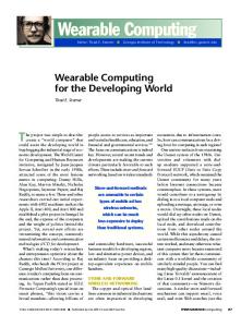
Abstract— This paper attempts to discuss a selective overview of some recent trends & concepts in the field of unconventional (non-Von Neumann) computing paradigms using emerging non-volatile nanoscale resistive memory technology (RRAM). Case studies for dedicated nanoscale hardware used in non-spike based machine learning (ML) driven architectures such as- (i) Extreme Learning Machines (ELMs) and (ii) Restricted Boltzmann Machines (RBMs) are considered.
I. INTRODUCTION Advent of cheap electronic sensors, cloud computing, IoT, smart devices, mobile computing platforms etc., has led to generation of enormous amounts of data. Some characteristics central to this big-data is its asynchronous and non-standardized nature. The vast amount of data by itself is of less value, however the ability to effectively and efficiently process this data in real-time leading to meaningful patterns, trends and interpretation is the real treasure-trove. Several upcoming unconventional (non-Von Neumann) computing paradigms, where memory (storage) and processing are not isolated tasks in themselves or rather memory is intelligent, offer promising capabilities to this problem of massive non-synchronous, non-standardized data treatment. Techniques such as software Artificial Neural Networks (ANNs), Artificial Intelligence (AI) and Machine Learning (ML) have been proving their mettle in fields as diverse as autonomous navigation, to robotics to analytics since a while. However the full potential of these computing paradigms can only be realized when they are directly implemented on dedicated low-power, compact, reconfigurable, programming-free hardware. When it comes to dedicated hardware some first contenders are CMOS-ASICs, DSPs, GPUs and FPGAs. However most of these implementations rely on a layer of digital (VonNeumann modified) abstraction even if some grass root computing arises out of purely analog traits. To this end, over the last few years there has been a lot of activity across research groups postulating efficient hybrid CMOS‘Nanodevice’ computing hardware architectures. The ‘Nanodevice’ in these hybrid systems cover a vast range of technologies such as- organic nanoparticle transistors (NOMFETs) [1], CNTs (carbon nanotubes) [2], atomic nanogap switches [3], silicon thin film transistors (TFTs) [4], spin based devices [5], to families of emerging non-volatile resistive memory (including PCM [6-10], CBRAM [12][13][20], OxRAM [14][15], theoretical Memristor [11], *Research presented in Section II is partially supported by, Department of Science & Technology, Government of India. Manan Suri is with the Indian Institute of Technology - Delhi, New Delhi, 110016, India (e-mail:
[email protected]).
978-1-5090-1493-4/16/$31.00 ©2016 IEEE
etc.). In particular the RRAM based hybrid implementations have gained a wide traction due to the promising attributes of RRAM devices such as (i) low-cost & simplicity of fabrication (ii) high density & 3D integration (iii) low-power dissipation and (iv) high endurance [16]. RRAM device evolution in memory industry has been widely propagated for simple bit-storage purpose, owing to storage based on reversibly programmable resistance states in an active switching layer, sandwiched between two metallic electrodes. The nanoscale intrinsic (cycle-to-cycle) and extrinsic (device-to-device) variability, stochasticity and unreliability found across all emerging non-volatile RRAM device families are undesired attributes for conventional memory (storage/NVM driven applications) community; that has hard constraints of 99.99 % yield, endurance > 1012 cycles, tightly controlled Ron/Roff/programming-current distributions, and high temperature retention of ~ 10 years. However, some of these undesired nanoscale effects (variability/stochasticity) have been recently exploited for realizing certain non-Von Neumann computing paradigms (neuro-inspired and more recently ML-inspired algorithms) in hardware efficient ways [13], [17-20]. Fig. 1 shows a strong increasing trend in the field of nanodevice research for unconventional computing applications.
Figure 1: Rising global research trend for resistive memory/nanodevice driven unconventional computing applications. (Data obtained from Web of Knowledge using the search expression combinations: Neuromorphic/Machine Learning/Synapse with Nanodevice or resistive memory or memristor or OXRAM or CBRAM or RRAM or STT MRAM or phase change memory).
280
Considerable work has been done on implementing neuroinspired STDP and variants of STDP algorithms on RRAM/memristive hardware [23]. Advent of more complex learning and weight update algorithms (beyond-STDP kinds), for example ML-inspired, the peripheral synaptic-circuit (or weight-circuit) overhead considerably increases. The use of RRAM as a synapse/weight alone is less justified in such a case. A more application-oriented approach is needed to further strengthen the case of nanoscale RRAM devices in such systems that exploit the device properties also for peripheral non-synaptic and learning circuitry, beyond the usual synaptic functionality. In this paper we outline two novel designs utilizing the inherent variability in RRAM devices to successfully implement modified versions of Extreme Learning Machines (ELMs) and Restricted Boltzmannn Machines (RBMs) in hardware. The ELM design utilizes device-to-device variability of CBRAM and OxRAM devices to implement random input weights. While the RBM design utilizes cycle-to-cycle variability of OxRAM devices to implement stochasticity in neuron activation. Both designs exploit the RRAM’s inherent variability as an advantage to implement learning in hardware. Section II outlines the non-spike based Machine Learning (ML) inspired implementations, of our hybrid CMOS-RRAM (i) Extreme Learning Machine (ELM) [17][18] and (ii) Restricted Boltzmann Machine (RBM) [19] architectures. Relevant RRAM device characteristics at play are discussed in the corresponding parts. Section III presents the discussion & conclusion. II. MACHINE LEARNING IMPLEMENTATIONS USING RRAM A. Extreme Learning Architecture (ELM) An ELM basically consists of- hidden layer synapses with randomly assigned weights, a hidden neuron layer with an infinitely differentiable activation function, and an output layer. ELM’s simple learning algorithm gives it a strong advantage in terms of speed when compared to SVMs and other bio-inspired algorithms [24]. Unlike other algorithms that try to assign hidden layer synaptic weights to some predetermined values while solving a QPP (Quadratic Programming Problem) for the output synaptic weights, (exSupport Vector Machines), or improve them over successive iterations (ex-Back propagation), ELMs use random distributions of input weights and hidden layer neuron biases, that remain fixed during learning. Use of fixed random input layer weights allows the ELM to obtain a very good generalization behavior, compared to other gradient based neural networks which explicitly try to tune all parameters. Fig. 2 shows our proposed hybrid CMOS-RRAM based ELM architecture. HfO2 and TiO2 based OxRAM devices were fabricated for this study, and their intrinsic resistance spreads were exploited to realize the ELM hidden layer weights and neuron biases. The proposed architecture consists of following sub-parts – 1) Pre-Processing block: Stored images are first preprocessed by conventional filtering, digital-to-analog conversion (DAC) and normalization steps in this block.
Output of the pre-processing block is fed directly to a network of hidden layer synapses. 2) Hidden layer synapses: Implemented using either a crossbar (1R) or matrix (1T-1R) configuration of filamentary (HfO2) or interfacial (TiO2) OxRAM devices. Minimum size of the crossbar should be (N+1) x M; where N denotes the total number of input features (with one additional bias) and M denotes the total number of hidden layer neurons. RESET (or SET) operation is performed initially on the OxRAM synaptic matrix, before the launch of training- mode, to intentionally obtain a large spread of OFF (or ON) state resistance distribution. The variable OFF (or ON) resistance spreads give rise to random input layer synaptic weights. Exploiting intrinsic resistance spreads is area and energy efficient as use of costly extrinsic techniques such as random number generator or PRNG (pseudo-random) circuits are avoided. From a purely circuit/analog design point of view, choice of µ of ROFF distribution has an impact on power dissipation, voltages/currents of operation and line parasitic. µ would also determine the amount of current flowing in to the hidden layer neurons. 3) Hidden layer neurons: ELM learning algorithm can work with many infinitely differentiable activation functions such as sine, radial basis function, etc. We chose the sigmoid function as the hidden neuron for our architecture, based on the circuit implementation described in [22]. It was found that final learning/classification performance can be optimized by tuning the hidden layer neuron gain/sigmoidslope. Random neuron biasing can be achieved in an extremely area efficient manner by exploiting the hidden layer OXRAM synaptic matrix. 4) Training block: This block is active only during the training-mode operation of the network. In the training-mode, data is simultaneously fed to the pre-processing and the training blocks. For each training data point, the output of the hidden layer neurons and the expected output are stored inside the training block. The minimum size of training block memory is given by = No. of training samples x (No. of hidden neurons + 1) * Data bit width. Matrix inversion in the training block is performed, in order solve the linear system of equations and generate the synaptic weights for the output layer, using algorithms such as GaussJordan elimination or QR decomposition. 5) Output layer synapses: These are programmed only at the end of the training mode. These have a wide dynamic range. Thus implemented with purely digital weight representation. 6) Output neuron: In contrast to the hidden layer, which uses a sigmoid activation function, for the output neuron we make use of a linear activation function. To validate the proposed OxRAM-ELM architecture, full-scale learning and multiclass classification simulations were performed for two complex datasets: (i) Land Satellite images and (ii) Image segmentation. Mean classification accuracy of the system was found to be ~ 86 % and 95 % in the two cases respectively [17].
281
switching events was about ~ 8 million/per epoch. We found that switching energy dissipation and cycling endurance constraints scale up drastically with the number of training points, thus making RRAM a desirable candidate for the proposed hybrid RBM architecture.
Figure 2: The RRAM ELM Architecture [17], [18] B. Restricted Boltzmann Machine (RBM) Restricted Boltzmann Machines (RBMs) are widely used as building blocks for deep belief networks (DBN). They are useful in both supervised and unsupervised learning applications such as dimensionality reduction, classification, feature-learning etc. Fig. 3 shows our hybrid RRAM-CMOS RBM architecture. In our proposed hybrid RBM architecture, HfOx based (filamentary switching) RRAM devices were extensively used as: (i) Synapses (ii) Internal neuron-state storage elements and (iii) Stochastic neuron activation blocks. The system consists of 2 layers of stochastic sigmoid neurons (hidden and visible), all fully connected. The internal state (binary value) of each neuron is stored using individual RRAM devices. The neuron consists of a low-power 6-T CMOS sigmoid circuit [21], and a RRAM based stochastic activation block. Cycle-2-cycle intrinsic HRS and LRS variability of fabricated HfOx RRAM devices [17] is translated to stochastic activation, with the help of a comparator circuit. The synaptic array can be realized either with a crossbar or a matrix of RRAM devices. In the proposed scheme, each synaptic weight is realized using 4 binary RRAM devices (to obtain a 4-bit weight resolution). The weight update module is a purely digital circuit, that accesses synaptic weights and internal neuron states. It updates the synaptic weights during learning by applying the contrastive-divergence RBM weight-update algorithm. To validate the proposed scheme we simulated the RBM (Fig.1) for classification and reconstruction of hand-written digits on a reduced MNIST dataset of 6000 images. Simulated network consisted of 100 hidden layer- and 784 visible layer- neurons. Each visible layer neuron corresponds to a pixel in the image of the handwritten digit. For classification we added a third layer consisting of 10 output-neurons. Total required size of the RRAM matrix in the simulated application is of the order of ~ 4Mb. Final classification accuracy of 92 % was obtained over 50 training epochs [19]. Average number of RRAM
Figure 3: The OxRAM RBM Architecture [19]
III. DISCUSSION & CONCLUSION Clearly several concepts and ideas around hybrid CMOSRRAM computing architectures have been demonstrated recently. Innovations and system-level optimization has been achieved at different levels- at the device level, engineering the active switching material stack in some cases has led to multi-valued synapses. At times, in order to compensate for binary RRAM devices, the deterministic multi-valued learning rules have been adapted to binary probabilistic ones, or simple device redundancy has been used. For deterministic systems reversible non-volatile resistive switching and the ability to modulate resistance in a bidirectional fashion (both set-to-reset & reset-to-set transitions) is the underlying key RRAM device attribute. For probabilistic/stochastic systems, device stochasticity or unreliability has been exploited. These may include unwanted nanoscale effects such as- cycle-to-cycle switching failure, device-to-device spreads in Set/Reset current/voltage programming conditions, Ron/Roff values, and switching durations. It has been found that for overall system learning performance both in neuro- or ML- inspired architectures, activation function characteristics (or neuron outputs) driving the RRAM weight (or synaptic) elements may also be modified to further improve the performance. At circuit level trade-off exists between the amount of intelligence the peripheral activation node (or neuron) should have, as hardware area & power dissipation directly goes up with added functionality. Circuit level solutions also include multi-device synapses and complementary sinksource configurations to mitigate certain non-symmetric RRAM device behaviors. Thus tremendous optimization scope and different permutations exist for improving the recently proposed unconventional Hybrid RRAM-CMOS
282
computing architectures. The more urgent need of the hour is to fix and standardize certain performance parameters (example – activation functions, number of weight states etc.,) and benchmarking criterion for specific data-centric applications (example- visual, auditory etc.). ACKNOWLEDGMENT Work discussed in Section II was performed at IIT-Delhi in collaboration with CNRS & IEF-Paris (with contribution of V. Parmar, D. Querlioz and F. Alibart). The research presented above is partially supported by Department of Science & Technology (DST) research grant RP03051. REFERENCES [1]
F. Alibart, S. Pleutin, D. Gurin, C. Novembre, S. Lenfant, K. Lmimouni, C. Gam- rat, and D. Vuillaume, “An organic nanoparticle transistor behaving as a biologi- cal spiking synapse,” Advanced Functional Materials, vol. 20, no. 2, pp. 330–337, 2010. [2] A. K. Friesz, A. C. Parker, C. Zhou, K. Ryu, J. M. Sanders, H.-S. P. Wong, and J. Deng, “A biomimetic carbon nanotube synapse circuit,” in Biomedical Engineering Society (BMES) Annual Fall Meeting, 2007. [3] A. Nayak, T. Ohno, T. Tsuruoka, K. Terabe, T. Hasegawa, J. K. Gimzewski, and M. Aono, “Controlling the synaptic plasticity of a cu2s gap-type atomic switch,” Advanced Functional Materials, vol. 22, no. 17, pp. 3606–3613, 2012. [4] K. Cantley, A. Subramaniam, H. Stiegler, R. Chapman, and E. M. Vogel, “Spike timing-dependent synaptic plasticity using memristors and nano-crystalline silicon tft memories,” in Nanotechnology (IEEENANO), 2011 11th IEEE Confer- ence on, pp. 421–425, 2011. [5] Sharad, Mrigank, Georgios Panagopoulos, and Kaushik Roy. "Spin neuron for ultra low power computational hardware." Device Research Conference (DRC), 2012 70th Annual. IEEE, 2012. [6] M. Suri, O. Bichler, D. Querlioz, B. Traor ́e, O. Cueto, L. Perniola, V. Sousa, D. Vuillaume, C. Gamrat, and B. DeSalvo, “Physical aspects of low power synapses based on phase change memory devices,” Journal of Applied Physics, vol. 112, no. 5, p. 054904, 2012. [7] D. Kuzum, R. G. D. Jeyasingh, B. Lee, and H.-S. P. Wong, “Nanoelectronic programmable synapses based on phase change materials for brain-inspired com- puting,” Nano Letters, vol. 12, no. 5, pp. 2179–2186, 2012 [8] M. J. Breitwisch, R. Cheek, L. C.L., D. Modha, and B. Rajendran, “System for electronic learning synapse with spike-timing dependent plasticity using phase change memory,” United States Patent Application Publication, vol. US2010/0299297 A1, 2010. [9] M. Suri, O. Bichler, Q. Hubert, L. Perniola, V. Sousa, C. Jahan, D. Vuillaume, C. Gamrat, and B. DeSalvo, “Interface engineering of pcm for improved synaptic performance in neuromorphic systems,” in Memory Workshop (IMW), 2012 4th IEEE International, pp. 1–4, 2012. [10] M. Suri, D. Garbin, O. Bichler, D. Querlioz, C. Gamrat, D. Vuillaume, and B. Desalvo, “Impact of pcm resistance-drift in neuromorphic systems and drift-mitigation strategy,” in Nanoscale Architectures (NANOARCH), 2013 IEEE/ACM International Symposium on, 2013.
memristive devices: How should we model their behavior?,” in Nanoscale Architectures (NANOARCH), 2011 IEEE/ACM International Symposium on, pp. 150–156, 2011. [12] S. Yu and H.-S. Wong, “Modeling the switching dynamics of programmable- metallization-cell (pmc) memory and its application as synapse device for a neuro- morphic computation system,” in Electron Devices Meeting (IEDM), 2010 IEEE International, pp. 22.1.1–22.1.4, 2010. [13] M. Suri, O. Bichler, D. Querlioz, G. Palma, E. Vianello, D. Vuillaume, C. Gamrat, and B. DeSalvo, “ CBRAM Devices as Binary Synapses for Low-Power Stochas- tic Neuromorphic Systems: Auditory (Cochlea) and Visual (Retina) Cognitive Processing Applications,” in Electron Devices Meeting (IEDM), 2012 IEEE International, p. 10.3, 2012. [14] S. Yu, Y. Wu, R. Jeyasingh, D. Kuzum, and H.-S. Wong, “An electronic synapse device based on metal oxide resistive switching memory for neuromorphic compu- tation,” Electron Devices, IEEE Transactions on, vol. 58, no. 8, pp. 2729–2737, 2011. [15] Y. Wu, S. Yu, H.-S. Wong, Y.-S. Chen, H.-Y. Lee, S.-M. Wang, P.-Y. Gu, F. Chen, and M.-J. Tsai, “Alox-based resistive switching device with gradual resistance modulation for neuromorphic device application,” in Memory Workshop (IMW), 2012 4th IEEE International, pp. 1–4, 2012. [16] DeSalvo, B.; Sousa, V.; Perniola, L.; Jahan, C.; Maitrejean, S.; Nodin, J- F; Cagli, C.; Jousseaume, V.; Molas, G.; Vianello, E.; Charpin, C.; Jalaguier, E., "Emerging memory technologies: Challenges and opportunities," VLSI Technology, Systems, and Applications (VLSITSA), 2012 International Symposium on , vol., no., pp.1,2, 23-25 April 2012 [17] M. Suri, V. Parmar, G. Sassine and F. Alibart, "OXRAM based ELM architecture for multi-class classification applications," Neural Networks (IJCNN), 2015 International Joint Conference on, Killarney, 2015, pp. 1-8. [18] M. Suri and V. Parmar, "Exploiting Intrinsic Variability of Filamentary Resistive Memory for Extreme Learning Machine Architectures," in IEEE Transactions on Nanotechnology, vol. 14, no. 6, pp. 963-968, Nov. 2015. [19] Manan Suri, Vivek Parmar, Ashwani Kumar, Damien Querlioz, and Fabien Alibart, “Neuromorphic Hybrid RRAM-CMOS RBM Architecture,” IEEE Non Volatile Memory Technology Symposium (NVMTS), 2015, Beijing, China (in-press). [20] Suri, Manan, Damien Querlioz, Olivier Bichler, Giorgio Palma, Elisa Vianello, Dominique Vuillaume, Christian Gamrat, and Barbara DeSalvo. "Bio-inspired stochastic computing using binary CBRAM synapses." Electron Devices, IEEE Transactions on 60, no. 7 (2013): 2402-2409. [21] Pan, D., & Wilamowski, B. M. (2003, July). A VLSI implementation of mixed-signal mode bipolar neuron circuitry. In Neural Networks, 2003. Proceedings of the International Joint Conference on (Vol. 2, pp. 971- 976). IEEE. [22] Shi, Bingxue, Lu Chen, and Chun Lu. "Current controlled sigmoid neural circuit." U.S. Patent 6,664,818, issued December 16, 2003. [23] Serrano-Gotarredona, T., Masquelier, T., Prodromakis, T., Indiveri, G., & Linares-Barranco, B. (2013). STDP and STDP variations with memristors for spiking neuromorphic learning systems. In Frontiers in Neuroscience, Vol. 7, 2013. [24] G. B. Huang, Q.-Y Zhu, and C.-K. Siew, “Extreme learning machine:
[11] D. Querlioz, P. Dollfus, O. Bichler, and C. Gamrat, “Learning with
283
Theory and applications,” Neurocomputing, vol. 70, no. 1, pp. 489– 501, 2006.