and semiconductors (VOx, amorphous silicon, etc). The main thrust is to develop a technology that provides ultra low-cost thermal IR imagers. In this paper ...
Defence Science Journal, Vol. 59, No. 6, November 2009, pp. 580-589 Ó 2009, DESIDOC
REVIEW PAPER
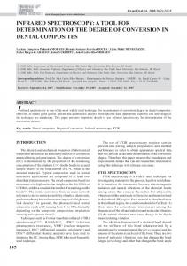
Uncooled Infrared Microbolometer Arrays and their Characterisation Techniques R.K. Bhan, R.S. Saxena, C.R. Jalwania, and S.K. Lomash Solid State Physics Laboratory, Delhi-110 054 ABSTRACT Recently, a lot of attention has been paid to infrared imaging using uncooled microbolometer detectors, primarily because of their low cost, and wide military and civilian applications. This paper reviews the basic principles of these detectors and some of the important works done internationally in this field. This paper presents some of the research work on titanium microbolometer carried out at Solid State Physics Laboratory, Delhi. Keywords: IR detector, bolometer, titanium, microbolometer, uncooled microbolometer detectors, infrared imaging
1. INTRODUCTION Infrared (IR) detectors are broadly classified into photon detectors and thermal detectors 1-3. Photon detectors are fast and more sensitive compared to the thermal detectors. As a result, these find applications in expensive weapon platforms, in astronomical observation instruments or in special medical instruments, where the performance is the main concern. On the other hand, the emergence of uncooled detectors4-31 has opened new opportunities for IR detection for both military and commercial applications due to their small size, less power consumption, and are less expensive, making these the ideal choice for applications requiring high unit numbers with relatively lower performance. The key factor in developing a highly sensitive detector is to develop a thermometer material compatible with silicon technology to achieve high thermal isolation in the smallest possible area. The microbolometer technology, well adapted for thin film process, leads to higher performance at the expense of more complex read-out integrated circuit design. The recent advances in microelectromechanical systems (MEMS) technology allow fabricating sensitive thermal bolometric detectors on thermally isolated hanging membranes. A bolometer employs a characteristic of thermally sensitive layer that changes its sheet resistance according to the change of the temperature (the larger the resistance change, the higher the temperature coefficient of resistance (TCR), so, higher of sensitivity). Many materials have been used for IR active layer of bolometer such as metals (Au, Pt, Ti, etc.) and semiconductors (VOx, amorphous silicon, etc). The main thrust is to develop a technology that provides ultra low-cost thermal IR imagers. In this paper, basic working principal of thermal detection and a comprehensive review of the microbolometer IR detector array technology with its characterisation techniques
have been presented. It also presents the work done at SSPL laboratory for the development of 16 x 16 titanium metal-film microbolometer arrays and their characterisation results. 2.
BASIC PRINCIPLE OF THERMAL DETECTION A bolometer measures the changes in the heat input from the surroundings and converts this into a measurable quantity such as a voltage or current. A bolometer therefore typically consists of an absorber and a thermometer, resulting in the increase in temperature due to absorption of IR radiations that ultimately causes a change in resistance of bolometer elements. The resistance change information is electrically transferred to the read-out integrated circuit (ROIC) for further processing. To obtain high sensitivity,
Figure 1. Schematic block diagram of a thermal detector (microbolometer).
Received 14 February 2009
580
Celebrating Sixty Years of Publication
BHAN, et al.: UNCOOLED INFRARED MICROBOLOMETER ARRAYS
the thermometer is kept thermally insulated with the ROIC substrate. The schematic block diagram of a typical microbolometer detector structure is illustrated in Fig. 1. The analysis of thermal IR detectors begins by solving the heat flow equation that describes the temperature increase in terms of the incident radiant power. The heat flow equation describing the pixel is:
d ( ÄT )
+G ( ÄT ) =çP=çPO exp ( jù t ) (1) dt where, C is heat capacity of the sensitive area of a pixel; G is thermal conductance of the support structure; P O is amplitude of modulated IR radiation power falling on pixel; h is absorbance of IR sensitive films; w is angular frequency of modulation of the radiation; and DT is temperature increase of the sensitive area of the pixel. This simplified equation assumes that the power dissipation in the sensitive area due to applied electrical bias can be neglected. The solution of Eqn (1) is: ç P exp ( jù t ) ç PO ÄT = O = 1/2 (2) G +jù C G 1+ù 2 ô2 where, t is the thermal response time. The temperature measurement is simplified when the resistance possesses a linear temperature dependence that holds true for most metals. For such a material, the resistance R can be expressed as C
(
)
R = R o {1 + a (TT o )} (3) where, R O is the resistance at the temperature T O and a is the temperature coefficient of resistance (TCR). The temperature increase, DT= TT o, due to the absorption of IR radiation is small enough so that the resistance change DR is linear with DT., i.e., or DR a DT
(4)
DR = a R DT (5) where, a = (1/R) dR/dt (6) The responsivity R v of an IR pixel is defined as the output signal (voltage or current) divided by the input radiant power falling on the pixel. Let the output signal be the voltage V s , then V s = I bDR = I b a R DT (7) where, I b is the bias current through the pixel. From Eqns (2) and (7), one gets
VS =
I b á Rç PO
G (1+ù 2 ô2 )
1/2
(8)
The responsivity (Rv) is defined by the following relation. R v = V S /P O (9) Hence,
RV =
I b á Rç
G (1+ù 2 ô2 )
1/2
(10)
Equation (10) shows that the responsivity is directly proportional to the temperature coefficient of resistance (a) and inversely proportional to the thermal conductance
(G) associated with the principal heat loss mechanism. Both parameters are important for uncooled IR resistive bolometers. The value of G can range over several orders of magnitude, whereas the range of possible values of a is far less. The primary focus should be on the thermal isolation structure. The choice of resistive material is also an important parameter and should be a secondary consideration. It should be compatible to the processing of sensor. Equation (2) is basic to thermal IR arrays. It describes the temperature increase of the resistive area of the pixel when radiation of power amplitude Po sinusoidally modulated with angular frequency w falls on the sensitive area. The pixel temperature increases and decreases as the input radiant power rises and falls in an oscillatory manner. The transition between the low and high frequency regions is characterised by the thermal time constant t or thermal response time, that is defined as: t = C/G (11) Another important parameter of thermal IR detector is detectivity and is given by (12) D*=(R v ÖADf)/V n where, Df is the detector noise bandwidth (Hz), V n is the total detector noise, and A is the detector area. The important measure of the performance of IR imaging system is noise equivalent temperature difference (NETD) that is the difference in the temperatures of objects in a scene, which will produce a signal-to-noise ratio of 1. It is given by
NETD =
4F 2Vn ôO ARV ÄP ÄT
(
)
ë1 -ë 2
(13)
where, F is the focal ratio of the optics and t O , is the transmittance of the optics, ( DP / DT ) ë1 - ë 2 is the change in power per unit area radiated by scene (or blackbody) at temperature T, wrt T measured within the spectral band from l1 to l2. Smaller NETD indicaties better performance. 3.
DESIGN OF BOLOMETER To obtain high performance, thermal arrays are designed in such a way so as to suppress the heat loss mechanisms. This is achieved by making the elements suspended using MEMS technology. The principal heat loss occurs only by the conduction through the support structure of suspended membrane to the substrate. The optimised support structure is the key to high performance thermal arrays. It provides three functions: mechanical support, a thermally conducting path, and an electrically conducting path. This structure can be fabricated by depositing thin films of selected materials like metals (titanium), vanadium oxide (VO x) or any other thermally sensitive resistive material on silicon substrate that incorporates a ROICs interface circuit at each pixel. To understand the electrical and thermal behaviour of bolometer, let the heat capacity of bolometer be C, connected by a small thermal conductance G, to a heat sink held at a fixed temperature T O, as shown in Fig.
Celebrating Sixty Years of Publication
581
DEF SCI J, VOL. 59, NO. 6, NOVEMBER 2009
Figure 2. (a) Schematic illustration of bolometer operation and (b) bolometer bias circuit.
2(a). Figure 2(a) shows the schematic illustration of bolometer operation and Fig. 2 (b) shows its bias circuit. The energy E of the incident radiation is converted into heat in the absorber, leading to a temperature rise D T = T T 0 = E/C, until the radiation power flowing into the absorber is equal to the power flowing into the heat sink through the weak thermal link. The temperature rise is subsequently measured and is directly proportional to the deposited energy. A constant current I, generated from the load resistor R L and bias voltage V bias, flows through the bolometer. Provided this bias power (P bias = V biasI) remains constant, the incoming signal power (Psignal), absorbed by the bolometer, will cause the bolometer temperature T to increase according to: T = T 0 + (P signal + P bias)/G. This temperature rise causes a change in the resistance of the bolometer and consequently in the voltage across it. This change in voltage is amplified and measured. The thermometer is therefore made of a material that ideally exhibits a large change in resistivity for a small change in temperature. The support structure is designed having excellent thermal isolation, that is, a very small value of G, expressed in W/ o C. Secondly, a detection mechanism and material are selected that, in combination with the support structure, provide high responsivity. Finally, the heat capacity C of the sensitive element expressed in J/oC is designed to be low enough to meet the response time (t) requirement. For example, for an array operating at the 30 Hz frame rate, the pixel response time should be shorter than 1/30 s. Common practice is to make the pixel response time one-third of the reciprocal of the frame time, say 10 ms. A structure, to design with G say equal to 1x10 -7 W/ o C, must have C equal to 1x10 -9 J/ oC to meet the response time requirement, i.e., t = C/G = 10 ms. The pixel area is defined by system requirement. Now, the adjustable parameter is only the element thickness. Assuming a 50 µm pixel attaining a value of C = 1 x 10⁻⁹ J/oC will require a thickness of the sensitive layer not more than 1µ for most of the materials. Thus, a membrane should be of the order of 1µ thickness or less. 582
The thermal time constant, t, as defined by Eqn (11) is the final performance parameter determining the spatial resolution of a thermal imaging system. The total thermal capacitance, C is given by (14) C = A (r 1 c 1d 1 + r 2 c 2 d 2 + r 3 c 3 d 3 +
.) Here, r, c and d, the density, specific heat, and material thickness, respectively of the different material layers of the pixel element. For example, for the design that contains the stack of Si 3N 4, Ti and TiN, one gets C= VrC ( Si N ) + VrC (Ti) + VrC (TiN) (15) where, V is the volume. The total thermal conductance (W/o C) given by 3
4
G = G leg + G rad + G gas (16) where, G leg is thermal conductance due to leg, i.e., support structure, G rad is thermal conductance due to radiation and G gas is the conductance due to gaseous conduction. The thermal conductance due to support structure, i.e., from leg (G leg) is the dominant conductance in comparison of conductance through radiation and conductance through gas. Thermal conductance, G leg, due to leg which connects the pixel element to silicon substrate to first approximation, is given by G leg = KA/L (17) where, K is the thermal conductivity, A is the area, and L is the length. Equation (17) can be used in several conductance paths of different materials each component being added to obtain the total conductance for example of Ti-bolometer silicon nitride (Si 3N 4 ) membrane or silicon dioxide (SiO 2 ) membrane and passivation with the same material layers and metal (Ti) electrode layer. The G leg for two legged structures is given as G leg = 2 KA/ L
(18)
G = 2K TiA Ti / L + 2K Si N A Si N /L (19) It is most important that the legs must constitute of material layers only having mechanical support and thermal IR detection electrode, which in the present case is the
Celebrating Sixty Years of Publication
3
4
3
4
BHAN, et al.: UNCOOLED INFRARED MICROBOLOMETER ARRAYS
Ti. Here, K Ti is thermal conductivity of titanium layer on leg (W/cmoC), K Si N is thermal conductivity of silicon nitride layer on leg (W/cm oC), A Ti is area of the cross sectional path of titanium layer on leg (cm2), A Si N is area of the cross-sectional path of silicon nitride leg (cm 2), and L is length of leg (cm). The response time t, can be adjusted by selecting appropriate values of the dimension of the legs of the support structures down which heat flows to the substrate. Therefore, to design a bolometer for certain value of t, time constant one has to compromise between leg length and membrane thickness. 3
4
3
4
4.
INTERNATIONAL SCENARIO AND RECENT DEVELOPMENTS Uncooled IR detectors are now available for various applications. Their simple operating conditions are similar to those of CMOS active pixel sensor (APS) or CCD digital camera. These have already shown their potential for many commercial and military applications. Nevertheless, as these are not cooled, so cold shield could be added to determine with precision the IR irradiance level. Consequently, these are very sensitive to temperature and environmental conditions and camera manufacturers have to take this behaviour into account to address thermographic applications by adding an internal temperature shield between the detector and the lenses. To fulfill this demand, a radiometric version of standard 320 x 240 detectors have been developed by M/S SOFRADIR and ULIS, France. There is persistent worldwide effort to implement very large format microbolometer uncooled IR detector arrays at low cost 5-25. For this, many researchers are trying to develop monolithic uncooled IR detectors with read-out electronics on CMOS wafer itself. The compatibility of the detectors with CMOS technology, to achieve this integration, is one of the main concerns for the development of lowcost detectors. Implementation of microbolometers on surface micromachined, bridges on CMOS-processed wafers is one of the most common approaches for uncooled IR imaging5-12. The bolometers are fabricated on these thermallyisolated and suspended bridges, as shown in Fig. 3. To improve the sensitivity performance, there are efforts to implement microbolometers using various materials,
Figure 3. Schematic of the bolometer approach employing suspended microbridges.
such as vanadium oxide (VO x)5-7, amorphous silicon (a-Si)810 , polycrystalline silicon-germanium (poly SiGe)11, 12, yttrium barium copper oxide (YBaCuO) 13, 14, and metal films15, 26. A high performance, very close to those of cooled infrared detectors, has been demonstrated with this approach, resulting in focal plane array (FPA) sizes as large as 640 × 480 and pixel sizes ranging from 50 µm down to 17 µm, especially using VOx and a-Si at much lower cost5-10. Another approach for highly sensitive micorbolometer is the use of silicon p-n junction diodes as the temperature sensitive element instead of resistive microbolometers in the detector arrays27-29. These are based on suspended multiple series diodes fabricated on SOI CMOS wafers, and successful implementation of 320 × 240 FPAs with 40 µm pixel pitch and 640 × 480 FPAs with 25 µm pixel pitch have been reported27-29. This approach provides uniform arrays with very good potential for low-cost, high performance uncooled detectors. However, its fabrication is based on a dedicated in-house SOI CMOS process, where intraCMOS MEMS process steps are included, limiting the cost reduction. The schematic of this approach is illustrated in Fig. 4.
ABSORBER LAYER
n-WELL
IN
R TE
CO
NN
E
YE LA CT
R
Figure 4. Si p-n junction diode microbolometers architecture.
Recently, a different approach has been proposed for very low-cost microbolometer array development, where the detector material is obtained with very thin Si/SiGe single crystal multilayers 30. Due to the high temperature epitaxial growth process, incompatible to CMOS read-out electronics, the material is grown on a separate substrate, and transferred on top of the CMOS read-out electronics using a 3-D integration process 30-31 , as depicted in Fig. 5. This approach, though provides a low-cost solution, requires a very complicated process with unconventional production methods that limit the yield. LETI and ULIS of France have chosen, from the beginning, to develop first, a monolithic microbolometer technology fully compatible with commercially available CMOS technology and secondly, amorphous silicon-based thermometer. This silicon approach has the greatest potential for reducing infrared detector manufacturing cost. After the development of the technology, the transfer to industrial facilities has been performed in a short period of time and the production is now ramping up with ULIS team in new facilities. LETI and ULIS are now working to facilitate the IR FPA integration into equipment to address a very large market 9-10 .
Celebrating Sixty Years of Publication
583
DEF SCI J, VOL. 59, NO. 6, NOVEMBER 2009
HANDLE WAFER
HANDLE WAFER
ROIC WAFER
ROIC WAFER
ROIC WAFER
ROIC WAFER
ROIC WAFER
ROIC WAFER
Figure 5. Schematic representation of 3-D integration of uncooled IR bolometer arrays: (a) Separate fabrication of ROIC and handle wafer containing bolometer material, (b) adhesive wafer bonding, (c) thinning of handle wafer, (d) bolometer definition (e) via formation, and (f) etching of sacrificial polymer adhesive layer.
Figure 6. Microbolometer IR detector arrays developed by ULIS: (a) SEM picture of bolometer element interconnection, and (b) packaged staring arrays.
Figure 6 shows the SEM picture and the packaging of the microbolometer IR detector array. For ultra low-cost applications, the latest trend is the implementation of the detector arrays together with their read-out circuitry on a standard CMOS or SOI-CMOS processing steps, using some simple post-CMOS etching steps, where neither any critical lithography nor any detector material deposition steps are needed. 5.
BOLOMETER ARRAYS DEVELOPED AT SOLID STATE PHYSICS LABORATORY The Solid State Physics Laboratory is engaged in the development of microbolometer-based IR FPA. Currently, the microbolometer arrays in 16 x 16 and 32 x 32 formats are under development. These are made using Ti as a bolometer material with TCR of about 0.25 per cent. Figures 7(a) and 7(b) show the schematic of the bolometer element 584
and the connection scheme in 16 x 16 arrays without using ROIC. Figure 7(c) shows the SEM picture of the bolometer element. Cros-sectional view and the air gap of the element can be seen in the figure. This scheme reduces the number of pads required for accessing all bolometers. In this configuration, only32 pads are required while in the case of individual access, one needs 512 (2 x 256) pads. Also, it is very close to the actual array from the processing point of view. Due to this complex switching structure, all other bolometers form a network in parallel with the bolometer being accessed. This not only affects the apparent resistance of the element being accessed, but also causes the signal of an individual element to diffuse over the whole array. To get rid of this unwanted networking effect, we have developed a method for extracting elements from this complex network has been developed has been developed 33.
Celebrating Sixty Years of Publication
BHAN, et al.: UNCOOLED INFRARED MICROBOLOMETER ARRAYS
and IR absorbance. The measurement setups for electrical and radiometric measurements are shown in Figs. 8(a) and 8(b). C O M P U T E R
PARAMETRIC C ANALYZER
TEMPERATURE CONTROLLER
TEST DEWAR CONTAINING DUT
ROW/ COLUMN SELECT MUX
VACUUM PUMP
(a)
(a)
BLACK BODY (BB)
C H O P P E R
BIAS SUPPLY SWITCHING CIRCUIT
DUT DEWAR
VACUUM PUMP
BB AND CHOPPER CONTROLLER
LOCK-IN-AMPLIFIER
C O M P U T E R
(b)
Figure 8. Block diagram of: (a) electrical measurement setup and (b) radiometric measurement setup for microbolometer arrays.
Various measurements and the corresponding parameters are listed in Table 1. The details of these measurements and parameter extraction are discussed. Other than these conventional techniques, many advanced techniques have been reported in literature. These techniques employ ac electrical technique for parameter extraction, single electrical measurements, and non-optical methods for complete characterisation of bolometer IR detectors. The IV characteristics of the bolometer array are obtained using the setup shown in Fig. 8(a) at a stabilised temperature (normally 300 K, i.e., the room temperature). These characteristics
(b)
Table 1. List of measurements and associated parameters (c) Figure 7. 16x16 Ti-microbolometer arrays developed at SSPL: (a) SEM picture of a bolometer element, (b) photograph of a part of the array, and (c) connection scheme.
CHARACTERISATION TECHNIQUES In this section, the various measurements and their techniques generally used for characterising these arrays, as reported in literature11,16,32-34 are described. The measurements are generally performed on each individual element of the array to extract the performance parameters of the detector. For extracting the electrical and thermal parameters, like TCR, G and C, current-voltage characteristic behaviour has been analysed and for the extraction of responsivity and sensitivity parameters, radiometric measurements were performed. The electrical output, as a function of chopping frequency, was used to extract the thermal time constant
Measurement Electrical measurements
Parameters Information extracted Resistance mapping 1. Offset nonuniformity 2. Bad elements Current-voltage 3. Thermal characteristics conductance (G) 4. Thermal breakdown point Current-voltage 5. Temperature characteristics coefficient of tempeature resistance (TCR)
Radiometric measurements
Signal and noise measurements
6.
6.
7. Frequency response 8. of signal 9.
Celebrating Sixty Years of Publication
Specific detectivity (D*) Responsivity (R v) Thermal time constant ( t ) Thermal absorbance ( h )
585
DEF SCI J, VOL. 59, NO. 6, NOVEMBER 2009
(20)
Eliminating (T-T O) in Eqns (3) and (20), one obtains
1 1 á 2 = - I R R0 G
(21)
This implies that 1/R changes linearly with the I 2 and if 1/R vs I 2 is plotted, the slope of the line will contain the information of a/G ratio. This is used to extract the thermal conductance G of the bolometer. For small values of current, the self-heating, being very less, is not clearly visible in the characteristics. Thus, relatively high currents need be applied, but that may cause excessive heating and permanent damage. Therefore, this measurement requires the knowledge of maximum tolerable current by the bolometers. Using the current-voltage-temperature (I-V-T) data, the change in resistance as a function of temperature can be plotted and the TCR can be extracted using Eqn (6). By knowing the values of TCR and G, one may easily find C using Eqn (11). For evaluation of IR sensing capability, the signal of the bolometer elements is measeared for a calibrated IR radiation falling onto it, noise of those elements and frequency response. A source of IR radiation (blackbody) is used to generate this IR radiation, which is mechanically chopped, as shown in the setup in Fig. 8(b). The device under test (DUT) finds the radiation intensity changing with the chopping frequency. The detector elements are biased with a constant current source. The incident IR signal causes change in the detector resistance, which is converted in to the voltage change by the bias current and monitored by a lock-in-amplifier locked with the chopper frequency. This measurement provides various system- related performance parameters like D*, R V , t and h . The specific detectivity is calculated using the following relation: D* =
SNR Area*Äf Power
áç RI b G 1+ù 2 ô2
For extracting the t, the frequency response was normalised by its very low frequency value, R v0. The normalised responsivity (also called relative responsivity) is given by the Eqn (24) and may be used to find the value of t.
RV ( Normalised ) =
1
(24)
1+ù 2 ô2
After determining the value of t , one may also find, as all other parameters in Eqn (24) are now known. SSPL has performed the characterisation of a number of our bolometer arrays developed. Figure 9 shows the characterisation results and Table 2 summarises them. The details of measurement and result are discussed 34.
(22)
The electrical signal output for the given input power is decided by the detectors responsivity, which is calculated using following the relation: R V = output electrical signal/input radiation power (23) where, R V is the voltage responsivity, having units of volt per watt. Thermal time constant decides how fast the bolometer may respond, and that further sets the limit on frame rate 586
RV =
ES)
I 2 R = G ( T - TO )
of the imager. Therefore, if one keeps on increasing the chopping frequency, the bolometer will get less and less time to respond to the radiation falling on it, causing less signal output. If the signal (or responsivity) wrt the chopping frequency is plotted, one gets the frequency response. This curve will therefore contain information of bolometers response time, i.e., time constant. One may re-state the bolometers responsivity Eqn (10) by the following relation:
D*(JON
deviate from ohmic behaviour due to self-heating effects. The dissipated electrical energy I 2 Rt is converted to heat. A part of this heat is conducted through the supporting legs. A very small part of this heat is radiated into the surrounding atmosphere, and the remaining heat increases the bolometer temperature, and hence its resistance. This effect is known as self-heating. This increases the resistance according to the relation described in Section 2. Assuming that heat conduction through support legs is the only heat loss mechanism, following relation is obtained.
Figure 9. Characterisation results of a typical 16x16 Timicrobolometer array developed by SSPL: (a) D* bar chart, and (b) D* histogram.
Celebrating Sixty Years of Publication
BHAN, et al.: UNCOOLED INFRARED MICROBOLOMETER ARRAYS
ROICs has been presented. The method may be used for initial development and evaluation of detector process technology leading to the fabrication of large 2-D bolometer IR detector arrays. Finally, some results of microbolometers developed by SSPL have been presented. ACKNOWLEDGEMENT The authors would like to thank Shri P.K. Basu, Director, Solid State Physics Laboratory, Delhi for his constant support and encouragement to publish this work. Authors would also like to thank Ms Anita Aggarwal, Ms Kumkum Khurana, Mr Pratap Singh Rana, and Mr Amit Vishwakarma for their help in detector development.
Figure 9. Characterisation results of a typical 16x16 Timicrobolometer array developed by SSPL: (c) normalised frequency response, and (d) R-T curve to determine the TCR. Table 2. Measured values of various parameters Parameter TCR (%) Thermal conductance (µW/K) Thermal time constant(ms) Detectivity (x10 8 cm Hz 1/2/W)
Measured value Average Variation 0.27 0.162
0.24-0.30 0.160-0.172
9.91 1.44
9.72-10.60 0.77-3.19
Efforts are on to demonstrate the basic imaging in the laboratory conditions using 16 x 16 and 32 x 32 (under development) arrays with the help of external hardware in absence of a proper ROIC. The concept of the hardware used is discussed 35 . 7.
CONCLUSIONS Some important fundamentals and theory of microbolometer infrared detectors along with some international developments have been serviewed. The methods of characterising the microbolometer arrays. The characterisation of 16x16 Ti-microbolometer IR detectors without using
REFERENCES 1. Rogalski, A. Infrared detectors: status and trends. Prog. Quant. Elect., 2003, 27(2-3), 59-210. 2. Sizov, F.F. Infrared detectors: Outlook and means. Semicond. Phys. Quan. Elect. Optoelec., 2000, 3(1), 52-58. 3. Rogalski, A. HgCdTe infrared detector material: History, status and outlook. Rep. Prog. Phys., 2005, 68(6), 2267-336. 4. Tissot, J.L. IR detection with uncooled focal plane arrays. State of the art and trends. Optoelecronics Review, 2004, 12(1), 105-09. 5. Wood, R.A. Uncooled thermal imaging with monolithic silicon focal plane arrays. In Proceedings SPIEInfrared Technology XIX., 1993, 2020, 322-29. 6. Anh, N.C.; Shin, H.J.; Kim, K.T. ; Han,Y.H. & Moon, S. Characterisation of uncooled bolometer with vanadium tungsten oxide infrared active layer. Sensors Actuators A, 2005, 123-124, 87-91. 7. Jeromiek, H.; Renaud, M.; Swart, N.R.; Picard, F.; Pope, T.D.; Levesque, M.; Lehoux, M.; Bilodeau, G.; Pelletier, M.; Audet, D. & Lambert, P. Micromachined VO 2 -based uncooled IR bolometric detector arrays with integrated CMOS read-out electronics. In Proceedings SPIE-Micromachined Devices Components II, 1996, 2882, 111-21. 8. Vedel, C.; Martin, J.; Ouvrier Buffet, J.; Tissot, J.; Vilain, M. & Yon, J. Amorphous silicon based uncooled microbolometer IR FPA. In Proceedings SPIE-Infrared Technology Applications XXV, 1999, 3698, 27683. 9. Tissot, J.L. et. al. 320 x 240 microbolometer uncooled IR FPA development. In Proceedings SPIEInfrared Technology Applications XXVI, 2000, 4130, 47379. 10. Mottin, E.; Bain, A.; Martin, J.L.; Ouvrier, J.L.; Bisotto, B.S.; Yon, J.J. & Tissot. J.L. Uncooled amorphous silicon technology enhancement for 25 µm pixel pitch achievement. In Proceedings SPIEInfrared Technology Applications XXVIII, 2002, 4820. 11. Sedky, S.; Fiorini, P.; Baert, K.; Hermans, L. & Mertens, R. Characterisation and optimisation of infrared poly SiGe bolometers. IEEE Trans. Elec. Dev., 1999,
Celebrating Sixty Years of Publication
587
DEF SCI J, VOL. 59, NO. 6, NOVEMBER 2009
46(4), 675-82. 12. Dong, L.; Yue, R. & Liu, L. An uncooled microbolometer infrared detector based on poly-SiGe thermistor. Sensors Actuators A, 2003, 105, 286-92. 13. Wada, H.; Sone,T.; Hata,H.; Nakaki,Y.; Kaneda,O.; Ohta,Y.; Ueno, M. & Kimata, M. YBaCuO uncooled microbolometer IR FPA. Sensors Mater., 2000, 12(5), 315-25. 14. Jahanzeb, A.; Travers, C.M.; Butler, Z.C.; Butler, D. P. & Tan, S.G. A semiconductor YBaCuO microbolometer for room temperature IR imaging. IEEE Trans. Elec. Dev., 1997, 44(10), 1795-801. 15. Tanaka, A.; Matsumoto, S.; Tsukamoto, N.; Itoh S.; Endoh,T.; Nakazato, A.; Kumazawa,Y.; Hijikawa, M.; Gotoh, H.; Tanaka, T. & Teranishi, N. Silicon IC process compatible bolometer infrared focal plane array. In Proceedings International Conference on Solid-State Sensors and Actuators, 1995, 632-35. 16. Shie, J.S.; Chen,Y.M.; Yang, M.O. & Chou, B.C.S. Characterisation and modelling of metal-film microbolometer. J. Microelectromech. Syst., 1996, 5(4), 298-06. 17. Schaufelbuhl, A.; Schneeberger, N.; Munch, U.; Waelti, M.; Paul, O.; Brand,O.; Baltes, H.; Menolfi, C.; Huang, Q.; Doering, E. & Loepf, M. Uncooled low-cost thermal imager based on micromachined CMOS integrated sensor array. J. Microelectromech. Sys., 2001, 10(4), 503-10. 18. Hirota, M.; Nakajima,Y.; Saito, M. & Uchiyama, M. 120 × 90 element thermoelectric infrared focal plane array with precisely patterned Au black absorber. Sensors Actuators A: Phys., 2007, 135(1), 146-51. 19. Sabuncuoglu Tezcan, D.; Eminoglu, S. & Akin, T. A low cost uncooled infrared microbolometer detector in standard CMOS technology. IEEE Trans. Elec. Dev., 2003, 50(2), 494-502. 20. Eminoglu, S.; Sabuncuoglu Tezcan, D.; Tanrikulu, M. Y. & Akin,T. Low cost uncooled infrared detectors in CMOS process. Sensors Actuators A: Phys., 2003, 109(1-2), 102-13. 21. Fedder, G.K.; Santhanam, S.; Reed, M.L.; Eagle, S. C.; Guillou, D.F.; Lu, M.S.C. & Carley, L.R. Laminated high-aspect-ratio microstructures in a conventional CMOS process. Sensors Actuators A: Phys., 1996, 57(2), 103-10. 22. Liddiard, K.C. Thin film monolithic detector array for uncooled thermal imaging. In Proceedings SPIE, 1993, 1969, 206-16. 23. Tanaka, A.; Matsumoto, S.; Tsukamoto, N.; Itoh, S.; Chiba, K.; Endoh,T.; Nakazato,A.; Okuyama, K.; Kumazawa,Y.; Hijikawa, M.; Gotoh, H.; Tanaka,T. & Teranishi, N. Infrared focal plane array incorporating silicon IC process compatible bolometer. IEEE Trans. Elec. Dev., 1996, 43, 1844-850.
588
24. Eminoglu, S.; Tezcan, D.S.; Tanrikulu, M.Y. & Akin.T. Low-cost uncooled infrared detectors in CMOS process. Sensors Actuators A, 2003, 109, 102-13. 25. Shie, J.S. & Weng, P.K. Design considerations of metal-film bolometer with micromachined floating membrane. Sensors Actuators A, 1992, 33, 183-89. 26. Herring, R. & Howard, P.E. Design and performance of the ULTRA 320 x 240 uncooled focal plane array sensor. Proceedings SPIE, 1996, 2746, 2-12. 27. Ishikawa, T.; Ueno, M.; Nakaki, Y.; Endo, K.;Ohta, Y.; Nakanishi, J.; Kosasayama, Y.; Yagi, H.; Sone, T. & Kimata, M. Performance of 320 × 240 uncooled IR FPA with SOI diode detectors. In Proceedings SPIE-Infrared Technology Applications XXVI, 2000, 4130, 1-8. 28. Ueno, M.; Kosasayama, Y.; Sugino, T.; Nakaki, Y.; Fujii, Y.; Inoue, H.; Kama, K.; Seto, T.; Takeda, T. & Kimata, M. 640 × 480 pixel uncooled infrared FPA with SOI diode detectors. In Proceedings SPIEInfrared Technology Applications XXXI, 2005, 5783, 566-77. 29. Kimata, M.; Ueno, M.; Takeda, M.; & Seto, T. SOI diode uncooled infrared focal plane arrays. In Proceedings SPIE-Quantum Sensing Nanophotonic Devices III, 2006, 6127, 612 70X-1 70X-11. 30. Niklaus, F.; Decharat, A.; Jansson, C. & Stemme, G. Performance model for uncooled infrared bolometer arrays and performance predictions of bolometers operating at atmospheric pressure. Infrared Phy. Tech., 2008, 51(3), 168-77. 31. Niklaus, F.; Kälvesten, E. & Stemme, G. Waferlevel membrane transfer bonding of polycrystalline silicon bolometers for use in infrared focal plane arrays. J. Micromech. Microeng., 2001, 11(5), 50913. 32. Gu, X.; Karunasiri, G.; Chen, G.; Sridhar, U. & Xu, B. Determination of thermal parameters of microbolomters using a single electrical measurement. Appl. Phys. Lett., 1998, 72(15), 1881-883. 33. Neuzil, P. & Mei, T. A method of suppressing selfheating signal of bolometers. IEEE Sensors J., 2004, 4(2), 207-10. 33. Saxena, R.S.; Bhan, R.K.; Jalwania, C.R. & Lomash, S.K. A novel test structure for process control monitor for un-cooled bolometer area array detector technology. J. Semicond. Tech. Sci., 2006, 6(4), 299-12. 34. Saxena, R.S.; Bhan, R.K.; Jalwania, C.R.; Rana, P.S. & Lomash, S.K. Characterization of area arrays of microbolometer-based un-cooled IR detectors without using ROIC. Sensors Actuators A: Phys., 2008, 141(2), 359-66. 35. Saxena, R.S.; Bhan, R.K. & Aggarwal, Anita. A new discrete circuit for read-out of resistive sensor arrays. Sensors Actuators A: Phys., 2009, 149(1), 93-9.
Celebrating Sixty Years of Publication
BHAN, et al.: UNCOOLED INFRARED MICROBOLOMETER ARRAYS
Contributors Dr R.K. Bhan obtained his MSc (Physics) from Kashmir University, Srinagar, in 1982 and PhD (Physics) from Delhi University in 1994. He joined Solid State Physics Laboratory(SSPL), Delhi, as a scientist in 1984. Currently, he is involved in infrared detector characterisation. His research interests include MOS physics, CCDs, IR detectors, and FPAs. Mr R.S. Saxena obtained his BE (Electronics and Communication Engineering) from G.B. Pant Engineering College, Pauri Garhwal, India, in 1997, and MTech (Microelectronics) from the Indian Institute of Technology, Bombay, in 2003. He is currently working toward the PhD from the Department of Electrical Engineering, Indian Institute of Technology, New Delhi. Since 1998, he has been a Scientist with the SSPL, Delhi. His current fields of interest are: Power electronic devices, nanoscale VLSI devices, and infrared detectors.
Mr C.R. Jalwania obtained his MSc (Physics) from University of Rajasthan in 1973. He joined Defence Electronics Research Laboratory (DLRL), Hyderabad, in 1974 and worked on various defence projects. He moved to SSPL in 1981 and worked on the fabrication of silicon devices. His current areas of research include: Solar cells, p-i-n diode, semiconductorbridge, porous-silicon, and MEMS. Dr S.K. Lomash obtained his MSc (Physics) and PhD from Delhi University, Delhi, in 1971 and 1976, respectively. He joined SSPL, Delhi, as a Scientist in 1979. He worked on various solid state device fabrication and testing. His current research interests are: IR detector technology, MEMS technology, and characterisation of semiconductor devices.
Celebrating Sixty Years of Publication
589