the coprocessor has an input FIFO, output FIFO and sin- gle register called N-Reg. The controlling processor writes the dimension of the matrices into N-Reg.
VT Matrix Multiply Design for MEMOCODE ’07 Eric Simpson, Pengyuan Yu, Patrick Schaumont, Sumit Ahuja, Sandeep Shukla Virginia Tech Electrical and Computer Engineering Deptartment Blacksburg, VA 24060 {esimpson, peyu1983, schaum, sahuja, shukla}@vt.edu
Abstract This design presents a system optimized for complex matrix multiplications on the XUP Virtex-II board. Utilizing the GEZEL HW/SW co-simulation environment, the resulting system achieves ˜25x speedup over a standard software only implementation. Further system level optimization (with DMA) results in the same coprocessor being speedup by at least another order of magnitude.
1
Introduction
This design presents a system optimized for complex matrix multiplications (C = AB). The initial N ×N matrices A, B, and C are contained in DDR RAM. Where each matrix element is a 32-bit complex number with the most significat 16-bits representing the real component, and least significant 16-bits representing the imaginary component. The multiplier matrix (B) and the product matrix (C) both use a 16-bit two’s-complement fixed-point format for the real and the imaginary component. The multiplicand matrix (A) uses a 16-bit two’s-complement fixed-point format with a 14-bit fractional component.
2
latency for the command, 2-3 cycles to access the location, followed by the actual data transfer. By utilizing sequential memory locations, the data can be transferred in bursts and therefore minimize the command and access latencies. In addition, due to the DDR RAM’s pipelined, multibank architecture, linear bursts also hide the row precharge and activation time.
2.2
With the plan to perform linear scans through the RAM, 4 elements at a time (128-bits), the design also attempted to optimize the use of the FPGA’s hard resources. The VirtexII provides 136, 18-bit x 18-bit multipliers in the FPGA fabric, along with 136, 18 Kb SelectRAM+ blocks. To utilize these fast discrete resources, the design performed 32 complex multiplies and accumulates per cycle. Since a single complex multiplication requires four multiplications and 2 addition/subtractions, a total of 128 multiplications, and 64 addition/subtractions were performed per cycle. In addition, one accumulate was needed for each of the 32 real and imaginary components, resulting in another 64 addition/subtractions each cycle. Therefore, the final design utilizes 128 out of the 136 multipliers and performs 128 addition/subtractions per cycle.
Design 2.3
2.1
FPGA Resource Optimization
Algorithm Optimization
DDR Optimization
Since hardware accelerators are often IO bound, the design first aimed to optimize the DDR interface. The XUP Virtex-II board provides a 64-bit interface to the offchip DDR RAM. Due to the double data rate operation, the RAM can provide the FPGA with 128-bits of data per FPGA clock cycle. Therefore, since the FPGA can access 128-bits of data in the same time as 32, or 64, the design goal was to utilize blocks of 128-bits. In addition, linear accesses provide the greatest throughput to the DDR RAM. Each DDR access requires a 1 cycle
A matrix multiplication algorithm was devised to linearly scan through the RAM and perform 32 complex multiplications per cycle. The algorithm begins by sending eight blocks of A values (a block is 4 elements) to the coprocessor. The eight blocks are from subsequent rows in A. Next, a block from B is sent to the coprocessor. The four incoming B elements are multiplied by the first element in each row of the A, and each of the 32 partial C products are accumulated. After a full row of B has been processed, the next active elements in A are the eight elements in the subsequent columns. The
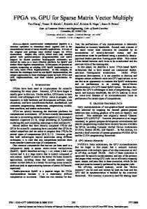
Figure 2. System with PPC in datapath Figure 1. Scalable Coprocessor Architecture process of sliding over B’s rows, and A’s columns is continued until the entire B matrix has been traversed. At this point, the complete product for the first 8xN elements of C has been computed and can be written back to RAM. The algorithm then repeats itself computing eight rows of C at a time until all of the C results have been calculated.
3
System Architecture
An interesting characteristic of the algorithm presented in section 2.3, is that the algorithm leads to a loosly coupled and scalable coprocessor architecture. As shown in Fig. 1, the coprocessor has an input FIFO, output FIFO and single register called N-Reg. The controlling processor writes the dimension of the matrices into N-Reg. For a given coprocessor configuration, N-Reg is the only control parameter that needs to be set at runtime. Based off the single N-Reg parameter, the coprocessor’s entire control FSM is determined. Therefore, in addition to a simple runtime configuration, the coprocessor’s control logic is captured by a low-overhead FSM. The coprocessor’s architecture also allows the designer to configure parameters optimal for their specific system. For example, Fig. 1 displays a coprocessor with a single MAC row. To implement a coprocessor that computes eight rows in parallel, a single design parameter is set to add the additional computational capacity. In addition to computational capacity, the internal datapath width to the “Aunit” and “MAC Unit” is configurable as well. In fact, a design was tested and verified with a configuration of (Aunit = 8x4, MAC = 8x4) and (Aunit = 16x4, MAC = 16x2) within minutes of each other. Therefore, the coprocessor architecture can scale to utilize a system’s available resources.
4
Methodology
The system was designed and implemented in the GEZEL environment. The software and hardware components were co-simulated and verified without VHDL level simulations being required. The fdlvhd tool was used to
Figure 3. System with DMA controlling datapath
convert the GEZEL FDL into the coprocessor’s synthesizable VHDL.
5
Results
The results from two system architecture implementations are shown in Table 1. Both system architectures utilize the same underlying interface to the coprocessor, but with different elements controlling the datapath to the coprocessor. In Fig. 3, the PPC retrieves the matrix data from RAM and then sends the data to the coprocessor. Therefore, in this scenario, the data is transmitted across the bus twice for every transfer. The resulting system is bottlenecked with 93% of the time spent performing IO operations. Moving the PPC out of the datapath results in a much more balanced system, with approximately equal time spent transferring and computing each block. The dramatic reduction results from two main factors. One, instead of each data item hitting the bus twice, each item is only transferred once. Two, the DMA controller is able to take advantage of both bus and DDR RAM burst access.
N 128 256 512 1024 1 Due
Table 1. Matrix Multiplication Results Ref Speedup SW SW / PPC SW / DMA1 PPC / DMA 0.7s 20.8x 67x 3.2x 5.3s 24.5x 132x 5.4x 42.0s 26.9x 264x 9.8x 338.0s 28.5x 1540x 54.0x
a bug with the Xilinx EDK 9.1 PLB DMA IP core, the DMA version was not submitted for final judging. While the DMA IP core transmits the correct amount of data and presents valid control signals, the IP core corrupts the transmitted data.