ISSN: 2250–3676
RAJESH SINGH* et al. [IJESAT] INTERNATIONAL JOURNAL OF ENGINEERING SCIENCE & ADVANCED TECHNOLOGY
Volume-2, Issue-2, 297 – 300
WIRELESS PERSONAL AREA NETWORK DESIGN AND SIMULATION TO LOCATE ACCIDENTAL INFORMATION USING 2.4 GHZ TRANSCEIVER MODULE Rajesh Singh1, Vivek Kaundal2, Arpit Jain3 1
Head, Robotics Institute R&D, Assistant Professor, University of petroleum & Energy studies, Dehradun,
[email protected] 2 Assistant Professor, University of petroleum & Energy studies, Dehradun, India,
[email protected] 2 Assistant Professor, University of petroleum & Energy studies, Dehradun, India,
[email protected]
Abstract With increase in automobile industry the roads are becoming more and more crowdie day by day. With the crowd the chances for accident are also becoming more versatile. These accidents cause very large loss of life and money. However lives could be saved if the information could be transmitted in time. In this project a system has been proposed which could transmit the information to the nearest help centre as soon as the accident occurs. The system uses wireless data transmission in ISM band frequencies. The system uses a microcontroller based system to transmit the system.
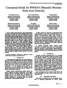
Index terms: Zigbee™, WPAN, ATMEGA 32 --------------------------------------------------------------------***-------------------------------------------------------------------------1. SYSTEM DESCRIPTION The proposed system uses an AVR core controller for coordinating the sensors and data transmission arrangement at both the transmitter and receiver side. The system is capable of transmitting the information to remote station within range of 100 meters. However the range can be increase as per requirement of a real time system and the cost of system. As soon as an accident takes place the information is transmitted to help centre by the microcontroller system at the accidental site. On the receiver side the information could be presented to the authority with the help of a suitable display device and an alarming system. In the given system the bump sensors are placed at suitable location inside the vehicle with the given arrangement. Data generated by the bump sensor is feed to the microcontroller as input. With the help of microcontroller data is processed and then write the suitable contents on LCD and also transmit the data through Zigbee transceiver module. The transmitting system is shown in figure (1.1)
Fig 1.1 block diagram of the transmitter module
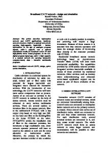
The data which is sent by transmitting station is received by the Zigbee module at receiving end and original data is extract from modulated data. Available data is read through controller and display through display system. We can also log the received data through RS 232 logic to PC with the help of
IJESAT | Mar-Apr 2012 Available online @ http://www.ijesat.org
297
ISSN: 2250–3676
RAJESH SINGH* et al. [IJESAT] INTERNATIONAL JOURNAL OF ENGINEERING SCIENCE & ADVANCED TECHNOLOGY suitable GUI like V1.9b Bray terminal or Mat lab or Lab view. The receiving system is shown in figure (1.2)
Volume-2, Issue-2, 297 – 300
MHz, allowing the system designed to optimize power consumption versus processing speed. D. LCD module -The LCD unit receives character codes (8 bits per character) from a microprocessor or microcomputer, latches the codes to its display data RAM (80-byteDD RAM for storing 80 characters, transforms each character code into a 5 ´ 7 dot-matrix character pattern, and displays the characters on its LCD screen. E. Transmitting module (ZigBee) - This is the radio frequency receiver module, which can facilitate the OEM designers to design their remote control applications in remote control in the quickest way. The circuit is designed with SMD components and the module size is small enough to be able to be fitted in almost any application. These modules are based on IC CC2500 by Texas Instrument. It works at frequency of 2.4GHz.
2.2 Receiving system design Fig 1.2 block diagram of the receiver module
2. HARDWARE DEVELOPMENT 2.1 Transmitting system design The transmitting node is in charge of collecting and transmitting bump sensor data, so it can be designed to Reduced Function device for reducing the power and cost. The chip CC2500and bump sensor constitutes the slave node. CC500 is the first SOC solution which supports the ZigBee protocol all over the world, an ATMEGA 32 MCU and a 2.4GHz wireless transceiver that suits to IEEE802. 15.4 standards are integrated inside. There’s an 2 KB random access memory in it, including 32 Flash storage unit, A/D converter, timer, watchdog timer, , meanwhile 1 UART interfaces and 32 programming I/O pins are contained in the chip. A. Power supply unit -this unit is basically designed to power up the transmitting system or slave node. This provides 5 V, 500mA output to drive the nodes. B. Sensing module- The bump sensor module is used for detecting accident. It can be used as pressure detector if put force on it. It works in 5Vand gives TTL output which can be directly given to microcontroller or to relay through a transistor. C. Microcontroller -The ATmega16 is a low-power CMOS 8bit microcontroller based on the AVR RISC architecture. By executing powerful instructions in a single clock cycle, the ATmega16 achieves throughputs approaching 1 MIPS per
The receiving system plays a coordinator role in the whole net, so it should be designed to a Full Function device; the main responsibilities of it are network establishing and maintenance, temperature data received in a wireless way, communication with the upper computer by serial port. We select CC2500 chip as the processor of the major-node, and expanding the serial communication port base on the CC2500 typical application circuit, MAX3232 chip is used to realizing level switch between TTL and RS232. A. Power supply unit- same as used in section2.1 B. Microcontroller- same as used in section2.1 C. LCD module - same as used in section2.1 D. Receiving module (ZigBee) - same as used in section2.1 E. Max 232(level converter)-The MAX232 is a dual driver/receiver that includes a capacitive voltage generator to supply EIA-232 voltage levels from a single 5-V supply. Each receiver converts EIA-232 inputs to 5-V TTL/CMOS levels. These receivers have a typical threshold of 1.3 V and a typical hysteresis of 0.5 V, and can accept ±30-V inputs. Each driver converts TTL/CMOS input levels into EIA-232 levels. F.USB to Serial cable- this provide the interfacing between coordinator node and personal computer G .personal computer- data logged off on PC with the help HyperTerminal and V1.9b Terminal
IJESAT | Mar-Apr 2012 Available online @ http://www.ijesat.org
298
ISSN: 2250–3676
RAJESH SINGH* et al. [IJESAT] INTERNATIONAL JOURNAL OF ENGINEERING SCIENCE & ADVANCED TECHNOLOGY
Volume-2, Issue-2, 297 – 300
3. SOFTWARE DEVELOPMENT Firmware for the modules has been developed with the help of WinAVR compiler and AVR studio. The controller is programmed with help of AVRDUDE. The software is written in C language and compiled using the open source compiler avr-gcc. For project management AVR Studio was used. I have used my fully buffered, interrupt driven USART library for usart related job. The library comes in two files. USART.c USART.h
Function to transmit and receive data Initialization of USART This function will initialize the USART. void USARTInit(uint16_t ubrr_value) { UBRR= ubrr_value; //Set Baud rate UCSRC=(1