This article has been accepted and published on J-STAGE in advance of copyediting. Content is final as presented. IEICE Electronics Express, Vol.* No.*,*-*
A 1.3V input fast-transient-response time digital low-dropout regulator with a VSSa generator for DVFS system Young-Jae Min1a), Chan-Hui Jeong2, Junil Moon2, Youngsun Han3, Soo-Won Kim1, and Chulwoo Kim1 1
School of Electrical Engineering, Korea University,
145, Anam-ro, Seongbuk-gu, Seoul, 02841, Korea 2
SK Hynix Incoporation,
2091, Gyeongchung-daero, Bubal-eub, Icheon-si, Gyeonggi, 17336, Korea 3
Department of Electronic Engineering, Kyungil University,
50, Gamsil-gil, Hayang-eub, Gyeongsan-si, Gyeongbuk, 38428, Korea a)
[email protected]
Abstract: A fast transient-response digital low-dropout regulator (D-LDO) is presented. To achieve fast-transient time, a VSSa generator and a coarse-fine power-MOS array techniques are proposed. The proposed D-LDO is implemented in a 65 nm CMOS technology with a die area of 0.067 mm2. The measured recovery time is less than 0.32 us when the load step-up time is 0.1 us from 2.5 mA to 120 mA, and the step-down time is 0.1 us at 1.2 V of supply voltage. Moreover, the voltage spikes are less than 190mV. Keywords: Low-dropout (LDO) regulator, Digital low-dropout (D-LDO) regulator, fast-transient-response time, dynamic voltage frequency scaling (DVFS) Classification: Power devices and circuits References [1] H.-C. Lin, et al.: “An active-frequency compensation scheme for CMOS low-dropout regulators with transient-response improvement,” IEEE Trans. Circuits Syst. II, Exp. Briefs 55 (2008) 853 (DOI: 10.1109/TCSII.2008.924366). [2] W. Oh and B. Bakkaloglu: “A CMOS low-dropout regulator with current mode feedback buffer amplifier,” IEEE Trans. Circuits Syst. II, Exp. Briefs 54 (2007) 922 (DOI: 10.1109/TCSII.2007.901621).
©IEICE 2017 DOI: 10.1587/elex.14.20170461 Received May 2, 2017 Accepted May 24, 2017 Publicized June 23, 2017
[3] T. Y. Man, et al.: “A high slew-rate push–pull output amplifier for low-quiescent current low-dropout regulators with transient response improvement,” IEEE Trans. Circuits Syst. II, Exp. Briefs 54 (2007) 755 (DOI:
1
IEICE Electronics Express, Vol.* No.*,*-*
10.1109/TCSII.2007.900347). [4] P. Hazucha, et al.: “Area-efficient linear regulator with ultra-fast load regulation,” IEEE J. Solid-State Circuits 40 (2005) 933 (DOI: 10.1109/JSSC.2004.842831). [5] M. Ho, et al.: “A low-power fast-transient 90-nm low-dropout regulator with multiple small-gain stages,” IEEE J. Solid-State Circuits 45 (2010) 2466 (DOI: 10.1109/JSSC.2010.2072611). [6] M. Al-Shyoukh, H. Lee, and R. Perez: “A transient-enhanced low quiescent current low-dropout regulator with buffer impedance attenuation,” IEEE J. Solid-State Circuits 42 (2007) 1732 (DOI: 10.1109/JSSC.2007.900281). [7] G. A. Rincon-Mora and P. E. Allen: “A low-voltage, low quiescent current, low drop-out regulator,” IEEE J. Solid-State Circuits 33 (1998) 36 (DOI: 10.1109/4.654935). [8] C. K. Chava and J. Silva-Martinez: “A frequency compensation scheme for LDO voltage regulators,” IEEE Trans. Circuits Syst. I, Reg. Papers 51 (2004) 1041 (DOI: 10.1109/TCSI.2004.829239). [9] P. Y. Or and K. N. Leung: “A fast-transient low-dropout regulator with load-tracking impedance adjustment and loop-gain boosting technique,” IEEE Trans. Circuits Syst. II, Exp. Briefs 57 (2010) 757 (DOI: 10.1109/TCSII.2010.2058590). [10] E. Beigne, et al.: “An asynchronous power aware and adaptive NoC based circuit,” IEEE J. Solid-State Circuits 44 (2009) 1167 (DOI: 10.1109/JSSC.2009.2014206). [11] Y. Okuma, et al.: “0.5-V input digital LDO with 98.7% current efficiency and 2.7-A quiescent current in 65 nm CMOS,” in Proc. IEEE Custom Integr. Circuits Conf., (2010) 1 (DOI: 10.1109/CICC.2010.5617586). [12] K. Mori, et al.: “Analog-assisted digital low dropout regulator (AAD-LDO) with 59% faster transient response and 28% ripple reduction,” in Proc. Int. Conf. Solid State Devices and Materials, (2013) 888 (DOI: 10.7567/SSDM.2013.H-2-4L). [13] Y.-C. Chu and L.-R. Chang-Chien: “Digital controlled low-dropout regulator with fast-transient and autotuning algorithms,” IEEE Trans. Power Electronics 28 (2013) 4308 (DOI: 10.1109/TPEL.2012.2230025).
1 Introduction The dynamic voltage frequency scaling (DVFS) techniques for multi-operating modes are appealing for use in an on-chip low dropout regulator (LDO regulator). The LDO regulator provides a stable voltage reference independent of input voltage variation, temperature, and time, while reducing wide fluctuations in upstream supply voltage and increasing the precision of the output voltage with few components. There are two categories of LDO regulator implementation in literature: analog and digital structures. The analog LDO can achieve a fast transient [1,2,3,4] and high power supply rejection ratio (PSRR) [5] within a smaller layout area with smaller power consumption [6,7]. Although it has many advantages, the analog structure faces many challenges. Under such a low voltage level, any parameter in the op-amp could further change the performance of the LDO. In addition, the analog LDO needs the use of a smaller output capacitor with low equivalent series resistance (ESR) in order to enhance the transient response
2
IEICE Electronics Express, Vol.* No.*,*-*
[8,9]. However, the use of analog design does not allow operation at low input and control voltages, and integration in digital functional unit is difficult. Moreover, the zero introduced by the small output capacitor may not be available for ensuring adequate phase margin. In this letter, the digital LDO with VSSa generator and a coarse-fine power-MOS array is proposed to achieve a fast-transient-response.
2 Previous digital LDO regulator The simplest digital LDO based on a discrete time (DT) control has an analog-to-digital converter (ADC) or digital control that converts the output regulated voltage to a digital word, and digital-to-analog converter (DAC) [10]. However, the analog-to-digital converter (ADC) and the digital-to-analog converter (DAC) blocks are still analog circuits. The digital LDO with digital comparator can operate at a low-voltage level (0.5 V) [11]. In addition, an analog-assisted digital low dropout regulator (AAD-LDO) can solve the problems caused by large output ripples in a conventional digital LDO [12]. A digital LDO with auto-tuning algorithms can achieve a fast transient using an auto-tuned voltage [13]. 1
Vlow Vhigh
2
Vlow Vhigh Vhigh≥ Vref ≥Vlow
‘HIGH’ state
Vhigh
Vcore= Vhigh-ΔV
Vlow
3
4
SoftSwitch
Vlow Vhigh Slow
Shigh CLK
Input data
Vcore= Ramp from Vhigh to Vlow or Vlow to Vhigh
Vcore C
Control
Vlow Vhigh ‘LOW’ state
Vref =Vlow
Vcore= Vlow-ΔV
Vcore= ~ Vlow
D→A
(a)
(b)
Fig. 1. (a) Block diagram of digital LDO with soft-switch, (b) Transition principle.
Fig. 1(a) shows a block diagram of a digital LDO with a soft-switch. It consists of a soft-switch, a clock generator, an op-amp, a control block, a DAC, and power MOSFETs (Shigh, and Slow). The soft-switch determines switching-on/off of power MOSFET (Shigh) whenever the output of LDO, Vcore, is changed. The clock in the clock generator operates the soft-switch and the control block. The op-amp compares Vcore and the output of DAC, which is a reference voltage. The control block modulates the soft-switch according to the output of op-amp and the DAC converts input data to a reference voltage. Fig. 1(b) shows the transition principles for changing Vcore. In 1-mode, the high values of power MOSFET (Shigh) are
3
IEICE Electronics Express, Vol.* No.*,*-*
switched on, while the others (Slow) are switched off; this is the ‘high’ state. Then, Vcore is equal to Vhigh - ∆V, where ∆V is the overdrive voltage, which is the highest voltage. In 2-mode, when the input data have a value between Vhigh and Vlow, Vcore also becomes a value between Vhigh and Vlow. The power MOSFETs (Shigh) are controlled by soft-switch on while the other MOSFET (Slow) is switched off. The soft-switch is used only in 2-mode. When input data is Vlow, LDO changes to the 3-mode, and the all power MOSFETs (Shigh, and Slow) are switched on. The low value of power MOSFET (Slow) is switched on while the other power MOSFETs (Shigh) are switched off; this is the ‘low’ state. Subsequently, Vcore is equal to Vlow ∆V, which is the lowest voltage. This ensures smooth transitions between Vhigh and Vlow without stopping the unit clock and computations. However, the op-amp and the digital-to-analog converter (DAC) blocks are still analog circuits, and their basic principle of operation is similar to that of the analog LDO. When using analog circuits, it is difficult to reduce the area as fabrication technologies advance in complexity. A low-input digital LDO consists of a bi-directional shift register, a switch array, and a comparator as illustrated in Fig. 2. Vin (0.5V)
Q1 Q2 Q3
VREF (0.45V)
Bi-directional shift registor
Q256
Vcore C
ILOAD
Fig. 2. Block diagram of Low-input-digital LDO.
Unlike analog LDOs, this digital LDO has a lot of power MOSFETs (switch array). The bi-directional shift register determines the switching-on/off of the switch array, and the resistance of the switch array is changed to control Vcore. The reference voltage, VREF, and the comparator determine the direction of the bidirectional shift register whether the value of Q [1:256] increases. This digital LDO eliminates all analog circuit, and is controlled by digital circuits. However, the digital LDO cannot operate at high load currents such as 100 mA, and cannot provide a quick response to a large load transient because of its shift-register based control method. Fig. 3(a) shows a block diagram of analog-assisted digital low dropout regulator (AAD-LDO). The AAD-LDO is composed a main digital LDO and sub analog LDO. The structure of main digital LDO is similar that of a low input digital LDO, and the analog LDO is an auxiliary LDO for fast-response. The digital LDO slowly controls Vcore with soft-switching in the controller to adjust coarse digital voltage step, and the analog LDO quickly changes Vcore with a fine analog voltage control to improve output ripple. However, because the digital LDO has an op-amp as an analog circuit, it also exhibits the stability issues of the op-amp. Fig.
4
IEICE Electronics Express, Vol.* No.*,*-*
Main digital LDO
Sub analog LDO
VREF (0.95V)
Controller
Vin (1.2V)
Q1 Q2 Q3
VREF (0.95V)
Q256
Vcore ILOAD
C
(a) Vin (1.8V)
Compensator
Vcore C
Dref Charge balance
+-
DAC
ILOAD
SAR ADC
Auto-tuning Fast-transient controller
(b) Fig. 3. (a) Block diagram of AAD-LDO, (b) Block diagram of digital LDO with auto-tuning algorithms.
3(b) shows a block diagram of a digital LDO with auto-tuning algorithms. This digital LDO consists of a power stage, a DAC in a successive approximation register (SAR) ADC, a compensator, a fast-transient controller, and a SAR ADC. In steady state, Vcore converts digital code DVout using the SAR ADC. This digital code is compared with a digital input Dref to generate a digital error De. Based on this digital error, the compensator generates a control code DVg to drive the power MOSFETs. Since the control code is digital, it needs to be transformed again by the SAR ADC to become an analog signal Vg. When a load transient is detected, a charge balance controller in the compensator quickly pulls the output voltage back to the reference voltage. Because different operating conditions may affect the efficacy of the fast-transient algorithm, an auto-tuning block sets coefficients in the fast-transient algorithm for an accurate output voltage. However, because it uses the SAR ADC and the DAC, it has a large area and large power consumption.
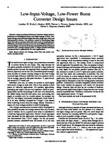
3 Proposed digital LDO The block diagram of the proposed digital LDO is illustrated in Fig. 4(a). It consists of a power-MOS array, two comparators, a control circuit with shift register and a VSSa generator. The power-MOS array is divided into a coarse array and a fine array. To improve a fast transient-response, the coarse array changes the output voltage Vcore by the digital code Coarse [6:0] from the DVFS system. The
5
IEICE Electronics Express, Vol.* No.*,*-*
VIN
Fine[0] Fine[1] Fine[7] Coarse[0] VSSa Fine[0] Fine[1]
VSSa
VSSa generator
Fine[7] Coarse[1] VSSa
Comp0
Power -MOS array
Comp1 Fine[0] Fine[1] Fine[7] Coarse[6] VSSa
Fine[7:0]
Coarse[6:0]
Comp0 SVSSa
Vref - 20mV
Dynamic Comparator
Control
Vcore
Comp Clocked Comparator
Shift register
Rload
Vref
Cload
Comp1 From DVFS system
EN
Dynamic Comparator
Clk
Vref + 20mV
(a) Coarse [6:0]
XXXXXXXX
1100000
1100000
Fine [7:0]
XXXXXXXX
11110000
11110000 11110000
1100000 11110000
11100000
11000000 11100000
11000000
11100000
CLKRX EN Comp
XXXXXXXX
1.2V
Vcore
1.10V 1.11V
1.12V 1.13V 1.12V 1.13V 1.12V
1.13V
(b) Fig. 4. Proposed digital LDO: (a) Block diagram, (b) Timing diagram.
fine array controls Vcore by using a comparator and a shift register. The comparators compare Vcore and Vref, which is converted from digital code in the DVFS system by the DAC. The shift register in the control circuit determines the switching-on/off of the fine-array. When a load transient is detected, the VSSa generator compensates for the ripple voltage. Fig. 4(b) shows the timing diagram of the proposed digital LDO. When the supply voltage in the DVFS system changes, Coarse [6:0] quickly pulls Vcore back to a revised Vref. Then, Fine [7:0] slowly tracks the revised Vref with a linear gate-width scaling of power MOSs. After Coarse [6:0] is entered, an enable signal EN is generated, and Fine [7:0] is started at the mid-point of Fine [7:0], “1111000”. The comparator checks whether Vcore is higher than Vref, and the output of the comparator, Comp, determines the direction of the shift register. When Comp is high, Fine [7:0] shifts to the left in order to increase the resistance of the power-MOS array. By contrast, when Comp is low, Fine [7:0] shifts to the right in order to decrease the resistance of the power-MOS array. To eliminate the timing issue, the comparator detects the voltage difference between Vcore and Vref at the falling edge and changes Fine [7:0] at the rising edge. After seven cycles of processing the changed supply voltage in the DVFS system, the control circuit sends an enable signal, SVSSa, to activate the VSSa generator.
6
IEICE Electronics Express, Vol.* No.*,*-*
3.1 Linear power-MOS array The proposed digital LDO uses a coarse-fine power-MOS array with linear resistance scaling. Because the resistance of the power-MOS is linearly scaled―the gate-width of the power-MOS is nonlinearly scaled, the dropout voltage attributable to the power-MOS is controlled accurately. The resistance of the power-MOS divided into the coarse array and fine array is determined by resistance, load current, and supply voltage as shown in Fig. 5.
Power-MOS resistance (Ω)
850
Coarse[0]
90 80 70
Coarse[1]
60 50
Coarse[2]
40 Coarse[3]
30 20
Coarse[4]
10
Coarse[5] 0.85V (0.5~2.5mA)
Coarse[6]
1.2V 1.05V 1.1V 1.15V 1V 0.9V 0.95V (4~14mA) (15~28mA) (30~48mA) (50~68mA) (70~88mA) (90~108mA) (110~128mA)
Fig. 5. Resistance of power-MOS array according to a load current and a supply voltage.
When the supply voltage is low (0.8 V), the load current becomes low except in the case of a line regulation or a load regulation. Similarly, when the supply voltage is high (1.2 V), the load current becomes high as well. Therefore, Coarse [6:0] determines the supply voltage and a range of load currents. When Coarse [6:0] is “1111111”, the power-MOS controlled by Coarse [6:0] turns off and a basic power-MOS operates. (A basic power-MOS is always turned on.) Then, the supply voltage becomes 0.8 V and the load current becomes 80 µA; this is sleep mode. The range of load current is 80 µA–128 mA and the range of supply voltage is 0.8 V–1.2 V. 3.2 VSSa generator Because Fine [7:0] is slowly changed by the shift register due to the slow operating frequency, it needs a compensation circuit to improve the load transient. The VSSa generator compensates for the slow load transient by controlling the gate voltage of the power-MOS. Fig. 6(a) shows the block diagram of the VSSa generator. The VSSa generator consists of a current source, NAND gate, and small capacitor. VSSa is 0 V within seven cycles after starting. After seven cycles, when Vcore is larger than Vref + 20 mV because of a varying load current, Comp1 becomes high-state. Since SVSSa is high-state after seven cycles, the output of the NAND gate becomes low-state, and VSSa increases rapidly by the current source due to small capacitor Ca as shown in Fig. 6(b). When Vcore is smaller than Vref – 20 mV, Comp0 becomes high-state, and VSSa decreases rapidly by the current source. The VSSa generator can compensate for the decreasing load current and the increasing load current.
7
IEICE Electronics Express, Vol.* No.*,*-*
Vin
VIN
Comp1 SVSSa
Fine[0] Fine[1]
VSSa Comp0 SVSSa
Fine[7] Coarse[0]
Ca
VSSa
(a)
SVSSa Comp0 Comp1
Vcore
Load transient Ref
VSSa 0V
(b) Fig. 6. Proposed VSSa generator: (a) block diagram, (b) timing diagram
3.3 Comparator and shift register In the LDO design, the large quiescent current degrades current efficiency of LDO. Thus, the low quiescent current is very important. In order to reduce the quiescent current, a clocked comparator is used in the digital LDO. However, because two static comparators for VSSa generator use the conventional comparator using a current mirror op-amp, the comparators have yet large power consumption. Fig. 7(a) shows the block diagram of a clocked comparator using a sense amplifier and a static comparator. In the clocked comparator, when Clk is low, the inputs to the NAND SR latch (A and B) are pulled high. When Clk is high, the inputs are compared to generate the output of the clock comparator. Fig. 7(b) shows the circuit implementation of the shift register. The shift register consists of MUXs and D-FFs. The shift-right or the shift-left operation of the shift register is determined by Comp. First, output of D-FFs, Fine [7:0], is set as mid-point, “11110000”, because Fine [7:4] set a “1” and Fine [3:0] resets as “0”. When Comp is low, Fine [3] moves to Fine [4], and Fine [7:0] becomes “11100000”, which achieves the shift-right operation. By contrast, when Comp is high, Fine [4] moves to Fine [3], and Fine [7:0] becomes “11111000”, which achieves the shift-left operation.
8
IEICE Electronics Express, Vol.* No.*,*-*
Clocked comparator
Vin
Clk
Static comparator
Vin
Clk B
A
Vcore
Vref A
ClkB
+
OUT
VBN
Comp
B
(a) Fine[0] Fine[1]
0
Fine[3] Fine[4]
Fine[4] Fine[5]
Fine[7]
1
D Q
D Q
D Q
D Q
S
S
R
R
Comp Clk Set
Fine[0] Fine[1] Fine[2] Fine[3] Fine[4] Fine[5] Fine[6] Fine[7]
0
0
0
0
1
1
1
1
(ii) Shift right 0
(i) Initialize
0
0
0
0
1
1
1
(iii) Shift left
0
0
1
1
1
1
1
0
(b) Fig. 7. (a) Block diagram of comparators, (b) Block diagram of shift register.
4 Experimental results The proposed digital LDO is fabricated with 65 nm CMOS technology for verification purpose. A microphotograph of the LDO is shown in Fig. 8. The active die area without the I/O pads is 0.067 mm2, which has the trade-off between the active area and the maximum load current. Fig. 9 shows the measured output of the LDO when digital code is updated to change the supply voltage. The step-up time is 0.1 µs from 1.2 mA to 120 mA, and the step-down time is 0.1 µs because the LDO requires converting time to change digital code to an analog signal. According to the digital code, the supply voltage and the load current are changed simultaneously. Fig. 4.11 shows the load transient. The load step-up time is 0.1 µs from 2.5 mA to 120 mA, and the step-down time is 0.1 µs at 1.2 V of supply
Driver VSSa Comp. generator
192 BMR
125
Power -MOS array
Shift registor 190
225
Fig. 8. Microphotograph of the chip
9
IEICE Electronics Express, Vol.* No.*,*-*
voltage. This time the recovery time is less than 0.32 µs. If Vcore has a large vibration due to a large variation in the load current, VSSa catches up to the changed Vcore as shown in Fig. 10(a) and 10(b). The voltage spikes are less than 190 mV.
Fig. 9. Measured output of proposed LDO
(a)
(b) Fig. 10. Measured load transient: (a) when a load current is changed from 1.2 mA to 120 mA, and (b) when a load current is changed from 120 mA to 1.2 mA.
10
IEICE Electronics Express, Vol.* No.*,*-*
5 Conclusion To summarize this study, performance comparisons with papers of digital LDO are listed in Table 1. Compared to those of the digital LDOs, though the quiescent current of the proposed scheme is the large due to three comparators, proposed scheme has smallest response time, 320 ns. Table 1 indicates that the proposed LDO can achieve fast response time for the DVFS system. The proposed D-LDO can work under low supply voltage and provide output voltage ranging from 0.8 V to 1.2 V for the DVS function. Experimental tests show that the proposed D-LDO not only is able to perform fast transient but also is capable of performing the DVS function. Table 1. Performance summary of LDO. This work
[10]
[11]
[12]
[13]
Type
digital
analog
digital
digital
digital
Tech
CMOS 65 nm
CMOS 0.18 μm
CMOS 65 nm
CMOS 0.18 μm
CMOS 0.18 μm
Minimum input voltage
1.3 V
-
0.5 V
1.2 V
0.9-1.8 V
Output voltage
0.8-1.2 V
0.8-1.2 V
0.45 V
0.95 V
0.8-1.5 V
Load current
80 µA -120 mA
-
0.2 mA
11 mA
200 mA
Response time
320 ns
500 ns
-
2.4 µs
2 µs
Decoupling capacitor
Not used
Not used
1 µF
10 nF
1 µF
Switching frequency Quiescent current Area Load regulation
16 MHz
-
1 MHz
1 MHz
5 MHz
1.5 mA
-
2.7 µA
14.2-242 µA 0.036 mm2 0.65 mV/mA
0.81 mm2
93.3-99.6 %
99.6 %
Current efficiency
2
2
0.067 mm
-
2 mV/mA
-
0.042 mm 0.65 mV/mA
98.75 %
-
98.65 %
-
Acknowledgments This work was supported by the Brain Korea 21 Plus Project in 2017.
11