Fujitsu Laboratories of America, Inc. ... miss. Thus, accessing the block will always cause a cache miss. Otherwise, the ..... Black dots represent results of our.
A Cache-Defect-Aware Code Placement Algorithm for Improving the Performance of Processors Tohru Ishihara and Farzan Fallah Advanced CAD Technology Fujitsu Laboratories of America, Inc. Sunnyvale, California 94085, USA Abstract— Yield improvement through exploiting fault-free sections of defective chips is a well-known technique [1][2]. The idea is to partition the circuitry of a chip in a way that faultfree sections can function independently. Many fault tolerant techniques for improving the yield of processors with a cache memory have been proposed [3][4][5]. In this paper, we propose a defect-aware code placement technique which offsets the performance degradation of a processor with a defective cache memory. To the best of our knowledge, this is the first compiler-based technique which offsets the performance degradation due to cache defects. Experiments demonstrate that the technique can compensate the performance degradation even when 5% of cache lines are faulty. In some cases the technique was able to offset the impact even in presence of 25% faulty cache-lines.
I.
INTRODUCTION
Most of today’s microprocessors including embedded ones employ one or more on-chip caches. Currently in most chips, caches occupy a large percentage of the area and the percentage is expected to increase in future. For example in StrongARM SA-110 processor, one half of the total chip area is devoted to the two 16KB caches [6]. Since cache arrays are designed with the tightest feature and scaling rules available in a given technology, they are more susceptible to faults compared to logic blocks [7][8]. Thus, the yield of microprocessors with on-chip caches can be enhanced considerably if cache defects are tolerated without noticeable performance degradation. Many techniques have been proposed for disabling faulty cache blocks in partially good chips [3][4][5][9]. Since using a smaller cache memory does not affect the correct operation of a processor, the processor can still be used after some changes even if the cache contains manufacturing defects. Therefore, the most straightforward solution to fix a chip with a faulty cache is to disable the entire cache. For set-associative caches, a possible solution is to disable the cache-way which contains the defect [9]. A more sophisticated way is disabling only the defective cache-line because the existence of a defect in a cache-line does not affect other cache lines. This can be done by using an extra bit added to the flag bits associated with each block and using the added bit for marking a faulty cache block [10]. If the bit is one, the corresponding cache
block will not be used for replacement in case of a cache miss. Thus, accessing the block will always cause a cache miss. Otherwise, the block is non-faulty and will be used. In this paper, we refer to the extra bit as FT-bit (FaultTolerance bit) [11]. Other names used in literature are: availability bit [3], the second valid bit [4] and purge bit [5]. The idea of adding the FT-bit was initially proposed in [10]. In this paper, we propose a defect-aware code placement technique which reduces the performance degradation of a processor with a partially good cache memory. We used FTbits in our technique. Our approach is to modify the placement of basic blocks or functions in the address space so that the number of cache misses is minimized for a given defective cache. To the best of our knowledge, this is the first compiler technique which reduces the performance degradation of a partially good cache memory. The rest of the paper is organized as follows. In Section 2, we summarize previous work and our approach. The definition of the problem and our algorithm for solving it are presented in Section 3. Section 4 presents experimental results. The paper concludes in Section 5. II.
PREVIOUS WORK AND OUR APPROACH
A.
Techniques for Recovering Cache Performance A replacement technique called the Memory Reliability Enhancement Peripheral (MREP) is presented in [12]. The idea is to have several spare words in a small set associative cache which may replace faulty words in the main memory. A technique similar to MREP is presented for on-chip caches in [13]. A very small fully associative spare cache is added to a direct-mapped cache and is used as a spare for the disabled faulty blocks. The experimental results in [13] show that one or two spare blocks are sufficient to avoid most of the extra misses caused by a few (less than 5%) faulty blocks. However, for a large number of faults, a few spare blocks will not be sufficient. Sohi [3] investigated the application of a Single Error Correcting and Double Error Detecting (SEC-DED) Hamming code in an on-chip cache memory. The idea of the SEC-DED approach is to use extra bits per word to store an
error correcting code and correcting data if a single error is detected [14]. The approach is effective for a single bit error per word (e.g., a single defect on a bit line) only.
Furthermore, no complicated hardware support like a Programmable Address Decoder (PAD) is required.
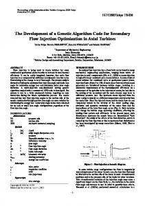
Shirvani et al. proposed a new cache architecture called PADded cache [11] which requires neither spare blocks nor error correcting bits. The idea is to recover the performance degradation due to faulty cache lines by mapping them to existing non-faulty cache lines. This is made possible by the use of programmable address decoder. Consider the direct mapped cache shown in Figure 1.
B. Conventional Code Placement We first explain the idea behind the conventional code placement technique. Consider a direct-mapped cache of size C ( = 2m words) whose cache line size is L words, i.e., L consecutive words are fetched from the main memory on a cache read miss. In a direct-mapped cache, the cache line containing a word located at memory address M can be calculated by (⎣M/L⎦ mod C/L). Therefore, two memory locations Mi and Mj will be mapped onto the same cache line if the following condition holds,
f0 a0 + f1 a1
f0
T0 f1 a0 + f0
a1
f1
T3
DATA
C ⎛ ⎢ Mi ⎥ ⎢ Mj ⎥ ⎞ =0 ⎜ ⎢ ⎥ − ⎢ ⎥ ⎟ mod L ⎝ ⎣ L ⎦ ⎣ L ⎦⎠
Cache-Line 1 TAG
f2
T2 f3 a0 + f2
Cache-Line 0 TAG
T1 f2 a0 + f3
FT-bit
DATA
Cache-Line 2 TAG
f3
DATA
Cache-Line 3 TAG
DATA
Several code placement techniques have used the above formula [16][17][18][19][20][21]. I-cache L=32 bytes
main memory A C
Figure 1. Programmable Address Decoder (PAD)
The number of sets is 4. Let a1a0 be the cache-line address. If a1a0 = 00, cache-line 0 is selected. If a1a0 = 01, cache-line 1 is selected, and so forth. Assume that cache-line 0 is faulty. The gates of transistors T0 and T1 are controlled using the FT-bit such that when cache-line 0 is marked faulty, T0 is always off and T1 is always on. As a result, all references to cache-line 0 are re-mapped to cache-line 1. Therefore, the addresses mapped to cache-line 0 are still cached, but they will have conflict misses with cache-line 1. By adding another FT-bit to the cache-line, it can be indicated whether both cache-line 0 and cache-line 1 are faulty. Thus, the second level of the decoder can be controlled and cache-line 0 and 1 can be mapped to 2 and 3 or vice-versa. The approach can be extended for set associative caches. Note the fault tolerance is achieved at the cost of higher complexity for the decoder which makes the cache-line access slower. Furthermore, there is a large area overhead due to adding FT-bits to each block. Note that FTbits must be implemented using flip-flops. One way to avoid adding extra bits is using the unused combination of the already available flag bits (e.g., valid bit = 0 and lock bit = 1) to indicate a fault in the cache-line. The lock bit is used to lock some or all contents of the cache in place. This feature is available on several commercial processors including PowerPC 604e, 405 and 440 families [22][23], Intel-960, some Intel x86 processors, ARM 10 family [24], NEC V830R processor [25] and so on. However, this results in performance degradation because it requires one extra cycle to read the FT-bits from the tag memory and configuring the address mapping. Unlike previous approaches, our approach needs neither any spare memory blocks nor error correcting codes.
(1)
conflict misses in cache-line 1
A
main memory A
B B
D
D
... ...
B
D
C ... ...
main loop
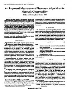
Figure 2. An Example of Code Placement
Assume a direct mapped cache with 4 cache-lines, where each cache-line is 32 bytes. Functions A, B, C and D are placed in the main memory as shown in the left side of Figure 2. If functions A, B, and D are accessed in a loop, conflict misses occur because A and D are mapped onto the same cache line. If the locations of C and D are swapped as shown in the right side of Figure 2, the cache conflict is resolved. Code placement modifies the placement of basic blocks or functions in the address space so that the total number of cache conflict misses is minimized. C. Our Approach Fabricated Chip
Target Application
Detect locations of defects
Generate a new object code or reuse an object code previously generated
Mark faulty cache-lines
Execute object code
Figure 3. Compiler Optimization Flow
Testing Phase Compiling Phase Booting Phase Running Phase
An overview of our approach is depicted in Figure 3. First, we detect the locations of defects in a cache memory. Next, our code placement technique generates the object code such that the number of cache misses will be lower than a given number. Therefore, we perform recompilation only if the original object code does not satisfy the required performance for a specific chip. If the original object code or an object code previously generated for another defect can satisfy the required performance, we use it. Every time the chip is turned on, it executes an initialization step during which based on the information collected during test, faulty cache-lines are marked using lock and valid bits. Then the chip executes the compiled code. Our approach exploits an unused combination of existing flag bits (i.e., valid bit=0 and lock bit=1) to indicate a fault in a specific cache-line. Assuming a 4-way set associative cache with lock and valid bits, if the lock bit of the way1 in the 5th cache-set is “1” as shown in Figure 4, the corresponding cache-line will not be used for replacement in case of a cache miss. If the valid bit of way1 in the 5th cacheset is “0”, accessing to the corresponding block will always cause a cache miss. Therefore, this mechanism guarantees the correctness of the processor operation even in presence of defects in tag or data memory. Lock bit Valid bit L V Tag0 0 1 2 3 10 4 5 01 6 7
Way0
L V Tag1
Way1
Manufacturing defect L V Tag2
Way2
L V Tag3
Way3
LV 01
01
LV 1 0
01 10
LV 0 1
where oi represents the i instruction of the original object code. Assume ai represents the address of oi. Each instruction oi is mapped to a memory block whose address is ⎣ai/L⎦. From the instruction trace we generate the trace of memory block addresses accessed, TMB = (b1, b1, b2, b3, …) We define X(bi) as,
⎧1 ⎪⎪ X (bi ) = ⎨ ⎪ ⎪⎩0
if there are at least Ws accesses to s = (bi mod S) between an access to bi and its next access otherwise.
where S and Ws are the number of cache-sets and the number of non-faulty cache-lines in the sth cache-set, respectively. The total number of misses can be calculated by,
Mtotal =
∑ X (b ) .
∀ bi ∈TMB
(3)
i
The above formula, which takes into account the effect of faulty cache-lines, is an extension of the formulae derived in [18]. Although the approach [18] results in many gaps in the object code (i.e., the memory requirement increases), our approach does not increase the size of object code.
LV 0 1
Cache Replacement Flow Figure 4. Cache Locking Function
Although most existing commercial processors do not allow to set the lock bit for an invalid cache-line (i.e., valid bit=0 and lock bit=1 is not a valid combination), supporting this combination is possible by a minor modification of the cache control circuitry. Note that for a set associative cache, the associativity of the cache-set which includes the faulty cache-lines is reduced by one. In a direct mapped cache, every access to the cache-set which includes the faulty cache-line will cause a cache miss. Our method modifies the placement of functions in the address space so as to compensate the increased number of cache misses due to faulty cache-lines. The most important feature of our approach is that it does not have any hardware overhead if the target processor has the cache lock function. III.
(2)
th
B. Trace Compaction For a given trace, it is usually possible to generate a shorter trace which results in the same number of misses, but can be processed faster.
10
1 0
(o0, o1, o3, o5, o6, o7, o3, o5, o7, o3, o5, o6, o7, o3)
PROBREM DEFINITION
A. Cache Miss Calculation We first generate an instruction trace corresponding to an execution of the application program as follows,
I-cache
main memory
cache line (L=32 bytes)
memory block (32 bytes) A function (104 bytes)
S=4 conflict misses in cache-line 1
... ...
Figure 5. An Example of a Self-Conflict Miss
Consider a function whose size is smaller than the cache size as shown in Figure 5. Left shows a direct mapped cache with four 32-byte lines. If a function whose size is 104 bytes is placed in the main memory, cache conflict misses occur in the cache-line 1 because the first and last words of the function are mapped onto the same cache-line. If the size of the function is 100 bytes, no self-conflict miss will occur no matter where in the address space the function is placed. Therefore, the condition for the self-conflict free function is as follows, The size of the function ≤ L×(S−1) + I
(4),
where L, S, an I represent cache-line size in byte, the number of cache-sets and instruction word size in byte, respectively.
C. Problem Formulation We summarize notations used in the problem formulation as follows, S: The number of cache-sets. L: Cache-line size in byte. Wi: The number of non-faulty cache-ways in the ith cache-set. Tc: The compacted trace of memory block addresses accessed. F: The list of functions in the target program sorted in descending order of their execution counts. Mtotal: The total number of cache misses. Mbound: The upper bound of the number of cache misses. This parameter is given by the user. The problem can be formally defined as follows: “For a given S, L, a set of Wis, Tc, F, and Mbound, find an order of functions, for which Mtotal is less than Mbound.” D. Algorithm Procedure Defect_Aware_Code_Placement Input: S, L, a set of Wis, Tc, F and Mbound Output: order of functions in the optimized object code Mmin = infinity; repeat for (t=0; t