Figure 2: The architecture of the Display Controller. The architecture ..... X_IP;+! EVAL2(1). XjPi+2. EVAL2(X,DX). XjPi+3. SETI(I). XjPi+4. SETI(X.DX}. Figure 11: ...
10 A Display Controller for an Object-level Frame Store System ~:~ JAK.S. Jayasinghe, A.A.M. Kuijk, and L. Spaanenburg
In [3] and [1] a new architecture for a Computer Image Generating (CIG) system designed to have optimal Interaction support for cealistlc 3D graphics has been presented. There it was stated that -from an interaction paint of view there IS no need to have access to an image representation as low as the pixel level. This. and the fact that the performance and resolution to a major extend has been limited by the pixe update speed enforced by memory technologies. led us to the conclusion that it should be investigated whether a CRT display could be refreshed fro·11 an object-level representation of the frame instead of the conventional pixel-level frame store. In thiS paper we present as a result of thiS study an architecture of a (multi-processor) Display Controlier that is capable to di'ectly refresh a raster display from such an Object-level frame representation.
CR Categories and Subject Descriptors: B.7.1 {Integrated Circuits] . Types and Design Styles VLSI C.l.m. [Processor ArChitectures] .' Miscellaneous - Hybrid systems C.3 [Special-Purpose and Application-based Systems} .' Rea/-time systems 1.3. t [Computer Graphics] .' Hardware Architecture - Raster display devices 1.3.3 {Computer Graphics]. Picture/Image Generation - Display algorithms Key Words & Phrases: Display Controlie', Computer Image Generation. Raster Graphics, Object Representation, MaSSive Parallelism. RISC, VLSI.
1. Introduction In present day workstations, high quality visualization and interaction facilities are becoming essential features. Recognizing this, system designers paid special attention to the image generation pipeline in order to improve both image quality and interaction behaviour. By improving the image generation pipeline, the frame buffer access bottleneck became more and more apparent. To overcome this problem, all sorts of partitioning * This study is partly funded by the Dutch Technology Foundation (STW).
142
strategies have been developed, without asking the basic question: "do we need a pixel level frame buffer?" The basic justification of a frame buffer in graphics systems is the need to uncouple the real-time refresh process from the computation intensive image generation process. In order to separate these two processes, storage of the image is needed in a representation suitable for the refresh process. Due to ever increasing demands on image quality and image complexity, even the vast evolution of hardware we could witness the last decade did not result in an image generating system that could meet the timing requirements imposed by the refresh process. This justifies the expectation that uncoupling of the image generating and the refresh process will always be needed. Realising this, the basic question posed above can be changed into: "do we need a frame representation level as low as the pixel level?" To answer this question from an interaction point of view an inventory of the types of graphics based interaction [3] shows that these interactions basically act on three representation levels (see Table 1). These levels are: Low: visible parts of objects (LDF). Medium: objects as a whole (MDF) and High: the image as a whole (HDF). Note that there are no interactions that address individual pixels at all. so the answer to the last question from interaction point of view is no. LDF
MDF
Highlight
Priority
BlinK
ViSibility
Depth Cue
Transparency
Pick
I
HDF
i Viewing Control
Grouping
Shading, Reflection
Scale, T ranslste, Rotate
Clip
Change, Replace
Table 1: Examples of some graphics based interaction operations and the representation lev els on which they operate. LDF is the level of visible parts of objects, MDF is the object level and HDF is the image level.
Based on this inventory, we designed a workstation architecture where all three levels mentioned are accessible for interaction purposes [1,3]. Since these three levels are present in our architecture, it is only a small step to come up with the final question: "is it possible to refresh directly from the lowest representation level needed for interaction?" In order to answer this question, firstly some details on this lowest representation level (LDF\
t
LDF stands for Low level Display File or alternatively Linear Display File following earlbom [2J
143 In our architecture, the LDF is a bucket-sorted structure of primitives called patterns It is the result of a hidden surface removal algorithm that operates in object space [5). It is essential to note that, since only the visible parts of objects are in this file, the patterns in this LDF are non-overlapping. The geometrical properties of these patterns are described by domains (O(x, y), in the form of a sorted list of slices designed for efficient HSR and scan conversion) whereas the colour properties are described by colourjunctions (C(x, y). What properties should a Display Controller (DC) have that can indeed refresh directly from this LDF, the lowest but still structured object-level representation we have accessible for interaction? It should be noted that since the number of patterns in the LDF can be very high for a complex scene (in the order of lOOK), the band-width of the LDF/DC interface will be a prime factor that could limit the performance of the DC. Because -as mentioned in the above- patterns in the LDF are non overlapping, only a few patterns, the so called Active Patterns, contribute to a given pixel-row. Active Patterns in general will contribute to several pixel-rows. Due to high refresh speeds, on-chip storage of the Active Patterns will be necessary to reduce the band-width requirements of the LDF/DC interface. Since each "slice" of a domain has enough information to paint the pixels up to the next slice, the on-chip storage could be kept to a minimum (i.e. instead of storing the complete active pattern in the on-chip storage, only one slice of an Active Pattern needs to be stored).
As real-time scan-conversion is a very demanding process, full exploitation of coherence so that incremental calculations can be done is essential. For each pattern, the colour of adjacent pixels as well as the intersections of the edges of a pattern with the next pixel row can be calculated incrementally. The exploitation of these coherencies of the patterns reduces the processing power requirements of the display controller dramatically (see the Appendix). Even with these incremental calculations several hundred MIPS are required for real-time scan-conversion. However, due to the technological limitations we have to face today, the capacity of processing elements will be limited to an order of 10 MIPS. Therefore, if we stick to the idea of refreshing from the LDF, the bandwidth requirements as well as the processing requirements enforce a multiprocessor implementation of the Display Controller. In this paper we present the basic structure of the Display Controller as shown in Figure I, designed with the above considerations in mind. The Display Controller consists of an Increment Processor (IP) capable of painting pixels on the display at refresh speed, an Active Patterns Store (APS) implemented as an on-chip memory of the IP, a high band-width LDF/DC interface, and a Pattern Loader (PL) which loads the active patterns from the LDF into the APS. Note that both the IP and the PL must be realized as multiprocessor arrays.
144
~
Incremental Processor (IP)
DC
V
G:) Figure 1: Functional block diagram of the Display Controller (DC). It consists of a Pattern Loader (PL) that loads the active patterns in the on chip Active Pattern Store (APS). These Ac tive Patterns are used by the Increment Processor (IP) to produce the pixel stream. Note that PL as well as IP are multiprocessor arrays.
2. A Multiprocessor Display Controller. During the design of the multiprocessor Display Controller, the following aspects have been taken into account. • Since all of the elements in the DC cannot be integrated into a single chip, the DC must be partitioned. This partitioning should not cause any considerable degradation of the DC performance. • The system should be scalable. That is, it should be adaptable to different resolutions and complexity demands. • The adaptability should show a performance improvement linear with the increase of hardware. • Ability to use the same architecture for increased packing densities (i.e. the architecture should not be determined by current VLSI technology).
145
•
Ability to handle images conslstmg of lots of small patterns having rather simple colour functions as well as images consisting of fewer patterns, but having more complex colour functions.
•
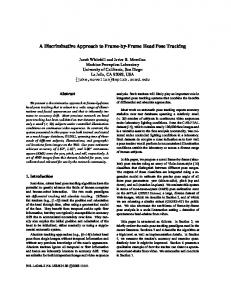
lmplementable in VLSL LDF
APS
rl-f --M _. --M V
seB
d~ J\ V
se Bus
V 0
APS: Active Pattern Store PL : Pattern Loader se : Scan-line Command SCB : se Buffer X IP : X Incremental Processor Y=IP : Y Incremental Processor
J\ V
oe
Figure 2: The architecture of the Display Controller.
The architecture presented in Figure 2 satisfies these requirements. This figure merely presents the data flow through the system. The control flow will be discussed in the next section. The high band-width of the LDF IDe interface, has been achieved by parallel accesses of the LDF by multiple PLs. Due to the fact that patterns in the LDF do not overlap, the PLs can work completely independently.
146
The nature of the DC process -incrementally generating streams of pixels, row by row suggests a splitting of these incremental operations in horizontal (x) and in vertical (y) direction. The y-increments to calculate both the intersection O(x) of a pattern with the current scanline as well as the colour function C(x) of that pattern on the current scanline. The x-increments to ealculate the pixel values of that section. Since the time constraints of these two processes differ in an order of the number of pixels on a scanline, it is reasonable to suggest an implementation of the IP array by two different types of processor elements, X_IP and Y_IP. The Y_IPs calculate the intersections of the pattern edges with the current pixel-row, the colour values at the left most edge, the incremental colour values along the pixel-row direction, etc, and generate from this the scanline commands that are sent into the Scanline Command Buffer (SCB). The X_IPs are pixel processors, of which there are as many as there are pixels on the pixel-row. The X_IPs are connected as a systolic-array. The left-most X_IP is fed by scanline commands from the Scanline Command buffers. Each X_IP performs incremental calculations on the scanline command it receives which is then passed on to its right neighbour. Depending on the type and destination range of a command, internal registers of the X_IPs are updated. Between commands from one scanline and the next, a special Refresh command is fed to the X IP array, which causes the X_IP that receives this command to output the resulting colour value and reset its internal registers to be able to start calculations for the next pixel-row. Since due to this mechanism Refresh commands directly control the pixel flush, they will have to come at regular intervals, dictated by the total line time. The architecture as presented in Figure 2 inherits the following features: • The number of X_IPs can be adapted to any display resolution desired. • The ratio of processor elements can be tuned to maximize the throughput of the DC. (e.g. if the throughput of a Pattern Loader seems to be larger than that of a YIP, one PL can be made to serve several Y_IPs.) • PLs and Y IPs can be added to the DC in order to increase the processing power. With this, the performance of the system can be increased up to a level where it can render the most complex pictures (i.e. pictures without any coherence between the pixels). • Realistic pictures "ith multiple light sources, and objects with diverse shading properties can be scan-converted in real-time. The realism of the generated picture can be improved by anti-aliasing the edges of the patterns (see the Appendix). As the processors in the systolic-array have to perform some calculations before they transfer data to their neighbouring processors, the transfer speed and consequently the maximum resolution is limited (with the targeted technology this will be in the order of 1 K X 1 K). Due to the anti-aliasing capabilities, the effective resolution of the display can
147
be improved beyond that. Alternatively, if a higher resolution is essential even without anti-aliasing, one can use a numbcr of X_IP arrays in paralleL As the speed of VLSI implementations is continuously increasing, it can be expected that within a few years time, also very high resolution displays can be refreshed using a single X IP array.
3. Partitioning the Multiprocessor Display Controller As sub-micron technology and wafer scale integration are not available on a cheap commercial basis, the DC has to be partitioned into several chips. As we mentioned before, this partitioning must not degrade the performance of the DC. Figur~ 3 shows the different levels of partitioning that can be done.
-_ ....•..........•
DC
....•••......... --- ....
Display
~
~
.. ! High priority Medium Priority Low Priority
Figure 3: The different levels of partitioning of the Display Controller.
148
As indicated by the thick dashed box, it would be desirable to have one complete, maximally configured, De in a single chip. This however is impossible, not only due to limitations of the silicon technology, but also due to the large number of I/O pins needed for a high band-width LDF IDe interface (which is realized by multiple busses). For this, the De can be partitioned as indicated by thin dashed boxes. This partitioning includes a PL and some Y_IPs on one chip, and the X_IPs on another chip. If even more partitioning is enforced by the technology available, we can do it as indicated by filled boxes. Here only a few X_IPs are integrated on one chip, the PL on a separate chip, and some Y_IPs with the APS on another chip.
4. Implementation of the Multiprocessor Display Controller 4.1. The Pattern Loader
As the output of the X IP array is directly used to refresh the display, the De will have to fulfill high throughput requirements. As a result programmability of the De must be kept to a minimum. On the other hand, in order to be able to adapt to future developments in lighting models, mapping techniques etc, we do not want to impose a severe restriction upon the representation in the LDF. Therefore any mismatch between the data representations in the LDF and the representations as needed by the increment processors must be resolved by a data dependent mapping, i.e. by making the PL programmable.
Program Memory I..
~I
RISC CPU
Figure 4: The basic block structure of the Pattern Loader.
Because of the high throughput requirements, calculations performed by the increment processors will have to be done using fixed-point numbers. Floating-point numbers, however, are indispensable for up stream processes in the image generating pipeline, such as the hidden-surface removal algorithm. As a resnlt, we propose the PL to be a pipe-lined RISe processor with a floating-point to fixed-point converter (preferably on-chip for maximum throughput). Since the LDF contains the data of the patterns, a separate memory is employed to store the RISe processor program. Figure 4 shows the basic blocks of the Pattern Loader. The data memory of the RISe processor consists of the LDF memory and APS memory. The PLs
149 will operate in MIMD (Multi-Instruction Multi-Data) mode, to be able to handle
differently structured data.
The function of the Pattern Loader (PL) is to transfer the active patterns from the Low
level Display File (LDF) into the Active Pattern Store (APS). The internal architecture of
the proposed RISC CPU. and it's instruction set are given in Figure 5 and Table 2
respectively. The estimated packing density is one PL per 1 p, CMOS chip. The number of
I/O lines connected to the PL is about 40. The PL could also be implemented using a
general purpose processor, probably at the cost of some performance degradation.
Functions to be performed by the PL's hardware are described in the coming sub-sections.
4.1.1. Program Loading Mode. In this mode the PML signal will be kept low by the host, and the PL':> program will be down loaded via the PL's data bus, otherwise used for LDF and APS memory access only. In this mode the normal operation of the PL will be suspended. Once the complete program memory is down-loaded. the PML line will be set on a high level again and the PL can start the pattern loading process. 4.1.2. Index Table Construction Mode. Although it may be possible to find the patterns contributing to the pixel-row being scan-converted on the fly, it is much more efficient to make use of an index table, i.e. a table, indicating which patterns are contributing to a given pixel-row. Modification of such an index table has to be carried out during the vertical retrace time, since at that time, no patterns are scan-converted. The index table can be stored in the LDF memory. There should be an entry in the index table for each pixel-row on the display and each entry of the index table must indicate which patterns become active on the pixel-row in question. This index table mechanism can be used to assure that pattern loading can be sustained at a sufficient rate. 4.1.3. Pattern Loading Mode. In this mode the active patterns indicated by the index table, will be transferred into the APS. As fixed-point numbers are used within the Display Controller, floating-point numbers will be converted into fixed-point representation. Complex patterns which, due to the fixed sized APS segments cannot be stored as a whole, must be decomposed into simple patterns. Sudden peaks in the pattern loading process can be minimized by loading patterns in advance. -- - The signals VAP, RE, GE and BE. are used to load the active patterns into the APS. The PL will lower the signal on the APSR line (by a RAPS instrnction) in order to get a free segment of APS memory. In return APSA will be lowered, if a free APS memory segment is available. The PL will wait for this signal if the WAPSA instruction has already BE and BE signals are used for selective transfer of colour been executed. The dependent data. Once an active pattern is loaded, the PL signals on VAP, indicating the incremental processors can scan-convert the pattern.
150 To I From LOF, APS
PC Add-Sub BA
APSA
Control
Register File
32 Bit x 16
INTA
32..1'
Barrel Shifter
DDB
Floating-point Fixed-point Converter I
I PI
LLC
ALU ...... RST
APSR BA BE GE INT INTA IRC LC LLC
APS Acknowledge
MUX PC PI RE RLC RST Temp
APS Request Branch Address Reg. Blue Enable Green Enable Interrupt Interrupt Acknowledge Increment LC Line Counter Last LC Reg. 2: 1 Multiplexer Program Counter Processor Identity Reg. Red Enable Reset LC Reset Temporary Reg.
VAP
Valid Active Pattern
Flags
APS Interface
t t t tt APSA APSR VAP
RLC ILC
FiE GE BE
Figure 5: Register level architecture of the Pattern LoadeL
The on-chip counter LC indicates which pixel-row is being scan-converted, whereby the PL can check whether it is loading the patterns in time. Such a check is needed, since a delay in the APSA signal might delay the PL. The LC counter is incremented by the signal on lIe and reset by RLe (Note that if a general purpose CPU is used for the PL, LC must be implemented in external hardware). If the patterns could not be loaded in time the host computer must be informed about this situation. The INT signal. generated by the OINT instruction, is used to report pattern loading problems to the host. The INT signal will transfer the value of the LC when the problem occurred (which is stored in LLC register) as well as a pattern identification number (which is stored in the PID register), when the host responds via tbe line INTA. In order to reduce the pin count of the PL, these data will
151 Genera! Control instructions
Data Transfer Instructions U)
liL
"[vi
Hi bits
NEG Ri
RI
-Ai
NOT Ri
RI
Not RI
OR RI, RI
RI
RI Or RI
SUB Ri, R)
RI
Ri-R)
SUBC RI, Rj
RI
RI-Rj-C
SUBI Ri, D
RI
Ri-D
SUBIC RI, [)
RI
RI-D-C
Table 2: Instruction set of the Pattern Loader, Ri, Rj are registers RO, R1" R15, "M and "Ri is the address given by M or Ri and