ESSCIRC 2002
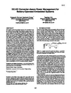
A Fast Response Adaptive DC–DC Switching Converter using On–Chip Dual–Loop One–Cycle Control Dongsheng Ma, Wing-Hung Ki and Chi-Ying Tsui Department of Electrical & Electronic Engineering The Hong Kong University of Science & Technology Clear Water Bay, Hong Kong SAR, China Fax: (852) 2358–1485 Email:
[email protected] Abstract A switching buck converter with variable output voltage using one–cycle control is presented. The control loop employs dc level shifting technique to eliminate the use of negative supply voltage. This controller accommodates both continuous and discontinuous conduction operation, and improves on existing open loop designs by adding a feedback loop for tight output voltage control. It was fabricated using a 0.5µm n–well CMOS process. The output voltage can vary from 0.9V to 2.5V, with a tracking time of 15µs for a step change of 1.2V. Efficiency is enhanced by a dynamic loss control, and a maximum efficiency of 93.7% is achieved with good line and load regulation.
the inductor current, which is very noise sensitive, and these converters normally have poor noise susceptibility. In this paper, we propose an integrated dual–loop one–cycle control variable–output switching converter. With this control technique, the converter is stable under all conditions, has no steady–state error, and has fast transient response. 2. On–chip one–cycle control with adaptive output 2.1 Principle of one–cycle control
1. Introduction Dynamic voltage scheduling (DVS) techniques have been shown to be the most effective methods in reducing power dissipation in digital systems [1]. Supply voltages are varied adaptively according to the loading of the system. In order to implement DVS techniques, multiple or variable on–chip supplies must be employed [2]. An adaptive voltage converter, compared with a fixed–output one, should have faster transient response to adapt to the rapid and large dynamic changes of the output voltage and load current. In the frequency domain, the dynamics of a switching converter depends on the locations of the poles and zeros of the closed–loop gain, which are functions of the output voltage and load current. If the changes of the output voltage and/or load current are large, the poles and zeros would vary accordingly, making the design of the compensation network extremely difficult. In the time domain, when the input supply voltage is perturbed, the duty ratio will not be adjusted until the error signal changes first. A typical transient overshoot will be observed at the output voltage and the converter takes a long time to reach the steady state. Conventional variable voltage control schemes employed worst case designs, resulting in a slow transient response, or controllers with very complicated designs [3~7]. In general, converters with current mode control have better dynamic performance. However, they need a current sensor to sense This research is in part supported by the Hong Kong Research Grant Council CERG HKUST 6209/01E
Figure 1. A buck converter with conventional one-cycle control
Fig.1 shows a buck converter with one–cycle control [8]. It is based on extracting information from the node vx instead of the output node Vo. When the transistor is on, vx = Vg. When it is off, vx = 0. The average value of vx is thus ( 1 / Ts )∫0Ts v x dt = ( 1 / Ts )∫0DTs Vg dt = DVg. If the converter works in continuous conduction mode (CCM), we have DVg = Vo. Hence, the output voltage can be controlled indirectly through monitoring vx. From Fig.1, The output of the integrator is vint(t) = –(Ts/CR) ∫0t v x dt , and the trip point is Vref = –(Ts/CR)DVg. Hence, Vo = – k1Vref with k1 = CR/Ts, which can be set equal to 1. The scheme is called one–cycle control because in every cycle, the integrated vx is set equal to a reference voltage Vref, and any perturbation in Vg can be corrected within one cycle. Therefore, it attains fast dynamic response. Because the converter has no dependence on past cycles, similar to employing dead–beat control, it is stable under all conditions. Previous implementations of one–cycle control converters all focused on fixed voltage regulation. Due to the nature of open loop control, the control equation can be satisfied cycle by cycle without waiting for the output to change. Therefore, the change in output is
379
governed by the dynamics of the power stage, not on the feedback loop. This feature is desirable for implementing a power source with variable output voltage, and the change is governed by the change in the reference voltage:
V
( s)
ref vo(t) = L−1 1 + ( L R) s + LCs 2 where L–1 indicates the inverse Laplace transform.
(1)
2.2 DC level shifting for on–chip implementation
X1 in Fig.2, the output of this integrator will be V1 = 1 2 Vg + 1 2 Vg D3 − 1 2 V g D − V0 D3 .
(6)
During D3T, Vo and Vg are both integrated, but the 2nd term in Eqn.6 should not appear in the integrator output. We solve this problem by replacing X1 and X2 in Fig.2 by those in Fig.4. Another opamp A11 in Fig.4 is added, and the corresponding output voltage Vc is given by Vc = 1 2 Vg − 1 2V g ( D1 + D3 ) . (7) Therefore, the output of X2 equals to V2 = V1 + Vc = V g − V g D − Vo D3 .
(8)
This modification allows the converter to switch between CCM and DCM smoothly.
Figure 2. Integrator with DC level shifting
Several drawbacks arise if the one–cycle control scheme is directly implemented on a CMOS chip. (1) The integrator uses a positive supply Vdd = Vg and an additional negative supply –Vss. All reported one–cycle control converters so far are implemented with discrete components that use both Vdd and –Vss. (2) A negative reference voltage has to be used. (3) It is an open loop control and the output voltage cannot be tightly regulated. A DC level shifting circuit in Fig.2 is proposed to solve the first problem. The integration of charge into C is now referenced to Vg/2 instead of ground to give V1(DTs) = (1/2)(Vg – DVg) (2) and simple analysis shows that V2(DTs) = Vg – (Ts/RC)DVg (3) V3 = Vg – Vref (4) which gives Vo = k1Vref. Now, instead of comparing DVg with Vref, we compare (Vg–Vref) with (Vg−DVg). Also, a positive Vref can be used. 2.3 One–cycle control extension to DCM converters For the converter to operate in discontinuous conduction mode (DCM), the one-cycle control scheme is still valid [8]. From Fig.3a, Vo is given by Vo = DVg D3Vo . (5) However, the DC level shifting technique in Fig.2 has to be modified: if the integrator in Fig.3b is used to replace
(a)
(b)
Figure 3. (a) Waveforms of buck converter in DCM, (b) a conventional integrator in DCM
380
Figure 4. An integrator for both CCM and DCM operation
2.4 Error correction loop for load regulation
Figure 5. Error correction loop
The original one–cycle control is an open loop control and cannot correct output voltage error. However, for adaptive applications, load regulation is very important. A change in load current will affect the output voltage immediately. For tight regulation of the output voltage, an error correction loop (ECL) in Fig.5 is added to this converter, which replaces the block X3 in Fig.2. Both upper and lower error voltage bounds r+ and r– can be set in advance. For Vref −r– < Vo < Vref + r+, the ECLs will be defeated. But if Vo > Vref + r+, Vo will be selected at node S1. An error voltage r = Vo − Vref will then be added to the reference voltage, which will be equal to Vg − (Vref + r) = Vg – Vo. As the reference voltage increases, the duty ratio of the converter decreases to lower the output Vo. When Vo < Vref −r–, a lower bound ECL functions in a similar fashion. 2.5 Dynamic loss control For a large load current, the power devices should be large to reduce conduction loss, but for a small load
current, they should be small to reduce switching loss. Efficiency is enhanced if the sizes of power devices could be adjusted accordingly. Such a dynamic loss control is implemented in this converter, which tailors for applications that a higher supply voltage (larger load current) is needed in the active mode, while a lower supply voltage is needed in the sleep mode. Since power transistors are built from smaller ones connected in parallel, some of the power transistors will be turned off as the output voltage drops. Note that the power diode in Fig.1 is implemented using nMOS transistor. 2.6 System Implementation
Figure 6. Schematic of the converter.
Fig.6 shows the overall schematic of the proposed converter. The integrator of Fig.4 is used here to allow the converter to work in both CCM and DCM. Error correction loops are installed to improve load regulation as discussed in Section 2.4. A multiplexer is used to select the reference level according to whether the output is larger than Vref or not. A voltage comparator across the nMOS power transistor works as a zero current detector [2] to determine the working mode of the converter and prevent the inductor current from going negative in DCM. 3. Experimental Results
Figure 7. Chip micrograph
The proposed converter has been fabricated in a standard 0.5µm n–well CMOS process. The chip micrograph is shown in Fig.7. The chip area is 2.31mm2. A 68µH inductor is used and the output capacitor is in the range of 1µF. Fig.8 shows the efficiency at different loadings and output voltages. High efficiency is obtained over a wide range with a maximum efficiency equal to 93.7%. Fig.9 shows the waveforms of the converter in
the steady state. The ripple voltage is less than 40mV, which is mainly due to large ESR and ESL of the filtering capacitor. Dynamic performance is measured using a test set–up shown in Fig.10. Test set–up (a) is used to measure the dynamic response as the reference voltage Vref varies. Fig.11 and 12 show the responses when Vref steps up and down by 1.2V, respectively. In both cases, the tracking times are within 15µs. The integrator output V2 and the inductor current IL are also shown. Test set–up (b) in Fig.10 is used to measure line regulation. Two DC power supplies differ by 1V are selected alternately as the input supply to the converter at 50kHz. Due to a large filtering capacitor Cin, the voltage Vg varies slowly rather than as a pulse train, as shown in Fig.13. Although Vg varies between 2.5V and 3.5V, the integrator adaptively adjusts its integration slope and the output voltage Vo stays almost constant. Test set–up (c) in Fig.10 is used to measure load regulation. Here, the load resistance changes periodically at 50kHz, which corresponds to a load current variation of 100mA. The results in Fig.14 show that the output voltage variation is less than 50mV. Finally, Table 1 compares this work with prior arts [3~7]. It shows that this design has a much better dynamic performance and a smaller chip area. 4. Conclusions An integrated dual–loop one–cycle controlled variable–output converter is presented in this paper. Design techniques that improve the control scheme and allow the controller to be realized on–chip are discussed. Experimental results show that the proposed converter has very fast dynamic response, good line and load regulation and high efficiency. 5.
References
[1] J. Rabaey, M. Pedram, Low Power Design Methodologies, Kluwer Academic Publishers, Boston, 1996. [2] D. Ma, W.H. Ki and C.Y. Tsui, “A pseudo–CCM/DCM SIMO switching converter with freewheel switching”, IEEE Int'l Solid–State Ckts. Conf., pp. 390-391, San Francisco, Feb. 2002. [3] W. Namgoong, M. Yu and T. Meng, “A high–efficiency variable–voltage CMOS dynamic dc–dc switching regulator”, IEEE Int'l Solid–State Ckts. Conf., pp. 380381, San Francisco, 1997. [4] G. Wei and M. Horowitz, “A fully digital, energy– efficient, adaptive power–supply regulator”, IEEE J. of Solid-State Circuits, pp. 520-528, April 1999. [5] F. Ichiba, et.al., “Variable supply–voltage scheme with 95%-efficiency DC–DC converter for MPEG–4 codec”, IEEE Int'l Symp. on Low Power Elec. Devices, pp. 54-59, 1999. [6] J. Kim and M. Horowitz, “An efficient digital sliding controller for adaptive power supply regulation”, IEEE VLSI Symp. on Ckts., pp. 133-136, Kyoto, June 2001. [7] M. Hiraki, et. al., “A 63µW standby–power micro– controller with on–chip hybrid regulator scheme”, IEEE VLSI Symp. on Ckts., pp. 225-228, Kyoto, June 2001. [8] K.M. Smedley and S. Cuk, “One–cycle control of switching converters”, IEEE Tran. on Power Electronics, Vol. 10, pp. 625-633, Nov. 1995.
381
Figure 12. Transient response when Vref steps down Figure 8. Efficiency of the converter
Figure 13. Line regulation performance
Figure 9. Waveforms of the converter in the steady state
Figure 14. Load regulation performance
Figure 10. Dynamic performance test set-ups
Table 1. Comparison with prior arts Tracking speed
Figure 11. Transient response when Vref steps up
382
Controller area @ CMOS process
Namgoong [5]