A HARDWARE / SOFTWARE CODESIGN METHOD FOR GENERAL PURPOSE RECONFIGURABLE COMPUTING Octavian CreŃ, Kalman Pusztai, Cristian Vancea, Balint Szente, Ligiu Uiorean Technical University of Cluj-Napoca, Computer Science Department, ROMANIA {Octavian.Cret, Kalman.Pusztai}@cs.utcluj.ro
[email protected],
[email protected],
[email protected]
Abstract: CREC is an original, low-cost general-purpose Reconfigurable Computer whose architecture is generated through a Hardware / Software CoDesign process. The main idea of the CREC computer is to generate the best-suited hardware architecture for the execution of each software application. The CREC Parallel Compiler parses the source code and generates the hardware architecture, based on multiple Execution Units. The hardware architecture is described in VHDL code. The VHDL source code is generated by a program, which was written in C. Finally, CREC is implemented in an FPGA device. The great flexibility offered by the general-purpose CREC system makes it interesting for a wide class of applications that mainly involve high intrinsic parallelism, but also other kinds of computations. Keywords: Reconfigurable Computing, Multiple Execution Units, FPGA, VHDL, ILP.
1. INTRODUCTION Programmable architectures heavily and rapidly reuse a single piece of active circuitry for many different functions. In configurable architectures, the active circuitry can perform any of a number of different operations, but the function cannot be changed from cycle to cycle. The most common examples are processors that may perform different instructions on their ALU on each cycle (for programmable devices), and FPGA devices (for configurable devices) [1]. The field of Reconfigurable Computing systems has known a significant development in the last years. Their efficiency has been proven in several types of applications, like DSP, image processing, pattern recognition, evolvable hardware, etc. In most projects, the main idea was to integrate a small processor together with a reconfigurable computing unit ([2], [3]) inside a single chip, thus achieving a considerable gain of performance for specific
applications, overcoming even the performances of specialized DSP processors. General-purpose reconfigurable computers (GPRCs) represent an (quite) old problem. A very important GPRC implementation was the DPGA [1], which basically consists of an array of reconfigurable computing elements (RCE), where the context memory of each RCE can store not only one (like in FPGAs), but several configuration contexts. This is a distinctive feature of all RC devices: the local storage of several configuration contexts for each RCE; it was adopted as a main characteristic of CREC. However, implementations of GPRCs are more rare. In this paper we introduce CREC (Calculator REConfigurabil): a GPRC with dynamically generated architecture, built in a Hardware / Software CoDesign manner. 2. MAIN CONCEPTS
The main idea of the CREC design was to exploit the intrinsic parallelism present in many low-level applications by generating the best-suited hardware for implementing a specific application. This way, there will be a different architecture implementing each application. The link between software and hardware is very tight: for each program written in CREC assembly language, the CREC environment generates the optimal architecture, that is then downloaded into an FPGA device (which constitutes the physical support of the CREC), and then the application is executed by it. We are thus building the CREC architecture without creating a specialized VLSI chip (like in most implementations of RC applications), but only by using existing tools and physical support: a VHDL compiler and synthesizer, a C++ or JAVA compiler, FPGA download programs and FPGA device(s). Even if the compilation time increases, for applications that need a big execution time, it will be largely recovered at run-time by the parallel execution instead of the classical, sequential one. This approach opens the way for a new family of computing systems, where there will be no restrictions on the number of execution units - EUs (there will always be a restriction given by the FPGA device capacity, but with the technological progress it will continuously increase, thus leading to more complex implementations of CREC-like architectures). 3. DESIGN FLOW The CREC architecture combines several architectural styles (RISC, DPGA, ILP-like multiple EUs) into a scalable structure. In fact, CREC is the final product of a Hardware & Software CoDesign process, where the hardware part is dynamically and automatically generated during the compilation process. The resulting architecture is optimal because it exploits the intrinsic application parallelism. The main steps in the application development are: 1. The application source code is written in a specific CREC assembly language, in RISC style. 2. The source code is compiled using a parallel compiler, which allows the implementation of ILP (instruction-level parallelism). The compiler detects and analyses data dependencies, then it determines which instructions can be executed in parallel (the program slices). Thus, the whole program is divided into slices; their size depends on the designed number of EUs used for program execution. 3. According to the slice’s size, the hardware structure will be generated that will run the program. The structure will be materialized in an FPGA device. The generic hardware architecture already exists in a VHDL source file, so at this moment it is only automatically adjusted according to the slice’s
size and some other options that will be discussed below. 4. The memory is divided in three parts. This is a quite different approach compared with other GPRCs. These parts are: Data Memory, off-chip; Instructions Memory, on-chip; Operands Memory, located on-chip or off-chip, according to the FPGA device capacity. 5. The VHDL file is compiled and the FPGA device is configured. 4. THE SOFTWARE DESIGN PROCESS The software part is implemented in two variants. The first one is written in ANSI-C and uses the BISON parser, without a user-friendly interface. In the second variant, the development software of the CREC computer is written in ANTLR and embedded in an integrated development system consisting of: the RISC Editor, the Parallel Compiler, the Instruction Expander and the Test Bench. The RISC Editor is a simple tool for writing RISC code to be compiled by the Parallel Compiler. Its main features are: Syntax help, Syntax checking, Save and load of RISC source files. The Parallel Compiler parses the CREC-RISC source code and determines the minimal number of program slices and also the instructions to be executed in parallel in each slice. Slices are a very important concept in the CREC compiler design. The instructions that are assigned to each EU to be executed at a same moment of time make up a program slice. The task of the Parallel Compiler is to determine the program slices. In order to do this, it analyses the data dependencies and applies a set of rules, which will not be detailed here by lack of space. An example of such a rule is: each slice can contain at most one LOAD, STORE or JUMP statement. Integrated CREC Development System
Application source code (written in CREC Assembly Language)
Application Execution
Parallel Compiler (determination of the number of slices and instructions scheduling)
FPGA Configuration Process
VHDL source code Generator (written in JAVA and ANTLR)
VHDL file Compilation
Fig. 1. The CREC design flow
The compiler reads the application source code (written in CREC assembly language) and generates a file in a specific format that describes the tailored CREC computer: the size of the various functional parts, the subset of instructions from the instruction
set involved, the number of EUs, etc., together with the sequence of instructions that makes up the program. The CREC Instruction Set was designed in RISC style. The number of instructions is relatively big; the arithmetic is performed only on unsigned integers, memory is accessed only through Load and Store; all operations are performed on data stored in the internal register. The usual arithmetic, logic, conditional data moving and conditional branching instructions are present, and the resulting CREC architecture will contain only the hardware needed to execute the subset of instructions used in the program. What makes CREC particular with respect to classical processors, besides its reconfigurable nature, is its the parallel nature: each register has an associated EU. Thus, at each moment during the program execution, there are N distinct EUs, each one running the instruction that was assigned to it. The compiler is the one that assigns the instructions to EUs, taking into account their nature and the rules associated with instruction scheduling. Some instructions specify which EU should execute them, while other instructions can be executed by any EU. For instance, “mov R1, 7” will be executed by EU1, since it works with R1, while “jmp 3” has no specific EU to execute it, and will be assigned one by the compiler, depending on the availability.
5. THE VHDL SOURCE CODE GENERATOR The information generated by the compiler is transmitted to the hardware structure by the means of a VHDL source file. Thus, after compiling the VHDL file, the different components of the hardware architecture are configured. The VHDL file contains an already written source code, where the main architecture’s parameters are given as generics and constants. This way, the hardware structure can be resized according to the needs of the application to be executed. The following components can be tailored: the number of EUs; the register width in each EU (all registers have equal width; so have the stacks, the load buffer and the store buffer); the size of the Instructions Memory; the slice-mapping block, containing instructions for each EU. This method allows to increase the operating speed and to the flexibility: the hardware architecture is resized according to application requirements. If a bus or Control Signal is not used, it will not appear, because no VHDL code will be created for it. Each EU is able to execute most common arithmetic and logic operations. Some of the operations might be useless for a specific configuration. In this case no VHDL code will be created for their implementation. The VHDL Source Code Generator needs the files provided by the Parallel Compiler, in the specific format established. The result will be several VHDL files describing the general CREC architecture. The generated VHDL source code can be compiled without any other adjustments. The whole design flow is fully automatic, i.e. the user involvement in this process is kept to a minimum. Hardware configuration is described using the generated VHDL code, which is also optimized using a package of programs. The optimization consists of eliminating each element, signal or bus from the final structure if not needed.
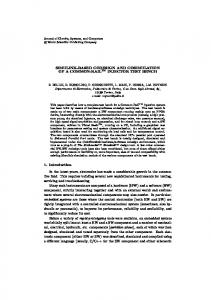
Fig. 2. CREC development system
All the EUs initially have an identical structure, and each one is able to execute any kind of instruction from the CREC Instruction Set. This means that the accumulators in each EU have equal capacities, but the internal structure of each EU will be different, according to the instructions subset (from the CREC Instruction Set) that each EU will actually execute. Having a greater number of EUs has the obvious advantage of introducing ILP, i.e. the execution of several instructions from the same program in parallel. The Test Bench is a simulator that allows the user to follow the execution steps, i.e. showing the instructions that are executed on each clock cycle by each EU.
6. THE HARDWARE ARCHITECTURE The hardware architecture is composed of: the N EUs; N local configuration memories for the N EUs, called Instructions Memories; a Data Stack Memory, used in instructions like PUSH or POP; a Slice Stack Memory, used to store the current slice address; a Slice Program Counter; an associative memory that maps instructions to the slices that must be executed by each EU, called Slice Memory; a Store Buffer and a Load Buffer (used to store information to/from Data Memory); a Data Memory; Operand Memories, containing the direct operands for the EUs. 6.1 The Instruction Set Each instruction is encoded on the same number of bits, like in RISC architectures. The instruction set is
The EU consists of: a Decoding Unit; a Control Unit; a Multiplexer Unit; an Operating Unit; an Accumulator Unit; a Flag Unit. The Operating Unit has a symmetrical organization. At the right side are the binary instruction blocks, and at the left side are the unary operation blocks. The four subunits are the following:
The conditions are: C (Carry), Z (Zero), E (Equal), A (Above), AE (Above or Equal), B (Below), BE (Below or Equal) and the negation of these with the N prefix.
Register MUX
Instruction Decoder
Input Port
Stack
Load Buffer
Instruction Code
Immediate Operand
Logic Unit – for the logical And, Or and Xor. It is composed of simple LUTs, 2 bits per slice. RN
•
R2
The Program Control Group contains instructions for altering the program execution. Each instruction is conditioned, thus offering a great flexibility: the source code can be optimized. Most of the Compare and Jump statements (the typical and frequently used instruction pairs) can be eliminated by the conditional instructions.. The instruction categories are: Slice counter manipulation (Jump, Call, Return); Data movement; Stack manipulation (Push / Pop); Input from / Output to port; Load / Store from the external memory.
but there was the need to increase the performance of the EU and to obtain almost equal propagation times. The second variant uses a general VHDL code, not optimized for any FPGA devices. This increases CREC’s portability, but the architectural optimizations become the VHDL compiler’s task, reducing the designer’s control over the generated architecture. In the next sections the Virtexoptimized architecture will be presented.
R1
divided in two groups: the Data Manipulation and the Program Control groups. The Data Manipulation Group contains the specific instructions for manipulating the value of the EU’s accumulator. The EU instructions are: Addition with / without carry; Subtraction with / without borrow and compare; Logical And, Or, Xor, Not and bit test; Shift arithmetic and logic to left or right; Rotate and rotate through carry to left or right; Increment or decrement the accumulator and negation.
Data MUX
Decoding Unit
Reg/Data MUX Multiplexer Unit
Addr
Addr
Addr
Addr
Addr
Addr
Instructions Memory
Operand Memory
Instructions Memory
Operand Memory
Instructions Memory
Operand Memory Shift Left Unit SHL/ROL/NEG INC/DEC/
Slice Memory
EU
EU
…
Logic Unit AND/OR/XOR
EU Shift Right Unit SHR/ROR/NOT
Arithmetic Unit ADD/SUB
Carry Generator
Slice Counter Operating Unit
DO
Addr
Load Buffer
Fig. 3. The general CREC architecture
The links between EUs are point-to-point (for example, these links are used when executing a “mov R1, R2” instruction), but the Data Memory, the Slice Counter, the Slice Stack Memory are accessed via Address, Data and Control busses. The Operand Memory can be accessed only by its corresponding EU.
CONDITION BUS
ZF
Control Signal Generator
Register
CF EXECUTION UNIT
DI
Data Memory
Condition Generator Flag Unit
Accumulator
CONDITION BUS
REG/DATA
Store Buffer
Control Unit
Data Stack Memory
JMP CALL RET PUSH POP LOAD STORE MOV STB W OUT
Slice Stack Memory
Register Value
Operand Value
Fig. 4. The basic CREC EU
6.2 The Execution Unit The main part of the CREC processor is the scalable EU. The word length of the EU is n*4 bits. At the current state of the implementation, the parameter n is limited to 4, so the word length can be up to 16 bits. There are two variants of the CREC EU implementation. In the first one, each subunit is strongly optimized for the Xilinx VirtexE FPGA family, occupying the same number of Virtex Slices (2*n Slices) and using the dedicated Fast Carry Logic. This leads to a platform-dependent solution,
Fig. 5. Block diagrams of the logic, arithmetic and shift units
•
Arithmetic Unit – implements Addition and Subtraction. The basic part is the two-bits adder, implemented in a single Virtex slice.
Fig. 9. The shift operations
Fig. 6. The ADD/SUB basic cell
•
Shift Left Unit – for the Shift and Rotate Left instructions paired with Increment or Decrement.
Fig. 7. The SHL/ROL/INC/DEC/NEG basic cell
•
Shift Right Unit – for the Shift and Rotate Right instructions paired with the logical NOT.
The output of the Flag Unit is a 6-bits wide Condition Bus for the six possible condition cases: Zero, Not Zero, Carry, Not Carry, Above and Below or Equal. This bus validates the conditioned Program Control instructions. The Multiplexer Unit is built on two levels for optimal instruction encoding. The Multiplexer Unit is also customizable. In VirtexE FPGAs, only 8-to-1 multiplexers can be implemented on a single level of CLBs. For this reason, the Multiplexer is optimized for up to 8 inputs. If the CREC architecture includes more than 8 EUs, than these multiplexers are implemented on two levels of logic. This disadvantage can be overcome if using larger capacity FPGAs where it is possible to implement wider multiplexers. The 2:1 bus multiplexer, which selects the output of the Data or Register Multiplexer, is implemented with tri-state buffers. The Accumulator Unit is built up from simple D FlipFlops. The Control Unit generates the validation signals for the Program Control instructions taking into account the Condition Bus. The Decoding Unit generates the appropriate signals for the functional parts of the Operating Unit. One EU uses only a fraction of the FPGA device. For example, an EU with 8-bits wide registers occupies approximately 4%, and an EU with 16-bits wide registers occupies approximately 6% of the available CLBs in a Virtex600E FPGA chip. 6.3 The Memories
Fig. 8. The SHR/ROR/NOT basic cell
All four subunits use the same number of slices, corresponding to 2 bits per slice. For this reason, the size of the Operating Unit is growing linearly with the word length. But the operating time will not decrease significantly with the increase of the word length, because the number of CLB levels is constant. Another important aspect is that the EU can be easily pipelined for higher frequency operation, using the Data Flip-Flops embedded inside the CLBs. For example, a complete EU (with all the subunits generated) having an 8-bit accumulator will consume 17 CLBs, but the same EU with a 16-bits accumulator will consume 33 CLBs.
The Slice Memory is an associative memory that stores the general slice word. This is composed of the slice words for each EU. A slice word contains two fields: the address of the instruction to be executed by the EU (a pointer in the Instructions Memory IM), and a pointer in the Operands Memory - OM. According to the number of instructions that each EU must perform, the width of the fields is variable and will be different for each EU. In the Virtex FPGA, this memory is implemented in the BlockRAMs. The instructions and the direct operands memories are distributed memory blocks, implemented in the Look-up Tables that are present in each Virtex slice. They are configured as ROMs. Their size depends on the number of instructions and on the number of
direct operands that each EU works with during the application execution. The size is optimized according to these parameters, in the VHDL code. The general Data Stack is implemented as a RAM. Its size is variable and will be estimated according to the number of Push / Pop instructions. The Slice Stack is used by Call and Return instructions. Here is stored the slice number when a procedure call/return from procedure call is performed. The Data Memory is normally implemented outside the FPGA chip, but for simulation purposes we created a Data Memory block inside the Virtex chip (in the BlockRAMs). 7. EXPERIMENTAL RESULTS At this point of the project, the software part of the CREC system is already finished, but can still be subject to modifications, as the Instruction Set will evolve and new features will be added. The parallel compiler is functional in two variants. The first variant is written in ANSI-C and uses BISON parser. The second variant is written in ANTLR and is integrated in an IDE; it has been tested and verified for some classical benchmark applications. The tests were performed on classical general-purpose algorithms. Some of the results are shown in Table 1. The algorithms were executed on CREC architectures having a different number of EUs; the reference architecture is the classical one, where an instruction is executed in each cycle. The performance indexes show how many times faster a given algorithm is executed on an optimized CREC system than in the case of classical execution flow (with one instruction executed per cycle). The efficiency of the CREC system is obvious for all kinds of algorithms. Higher improvements are obtained for DSP-like applications. Table 1. Performance evaluation of the CREC system CREC Optimized CREC Algorithm architecture Worst Best Bresenham’s line 3.00 3.00 CREC-10 Bresenham’s circle 4.08 4.60 CREC-12 Bubble sort 1.12 1.67 CREC-3 Quick sort 2.66 3.00 CREC-5 Map colouring 1.53 1.70 CREC-8 Integer square root 1.61 1.64 CREC-4 The hardware part of the CREC system has been implemented in some earlier versions (with a smaller, less complex instruction set and less architectural optimizations). The targeted FPGA device was a Xilinx VirtexE600. The physical implementation was made on a Nallatech Strathnuey + Ballyderl board, containing a Virtex 600E FPGA. Several CREC architectures were simulated and downloaded in this development system. A preliminary version of the CREC system having 4 EUs (CREC-4) with 4bits wide registers occupies 4% of the CLBs and 5%
of the BlockRAMs in the VirtexE600. A CREC architecture having 4 EUs with 16-bits wide registers occupies 18% of the CLBs and 20% of the BlockRAMs in the same device. The operating clock frequency is of 100 MHz. 8. CONCLUSIONS AND FURTHER WORK This paper presents CREC, a low-cost GPRC that combines hardware and software CoDesign. CREC exploits the intrinsic parallelism present in many low-level applications by generating the best-suited hardware for implementing a specific application. After generation, the architecture is downloaded into an FPGA, where the application is executed. CREC structure is basically composed of two main parts: the parallel compiler and the hardware structure, implemented by a Xilinx Virtex FPGA device. The physical implementation is made on a Nallatech board. The CREC computing system has been proven to be a very effective, low-cost reconfigurable architecture, allowing the execution of parallel applications with considerable performance improvements, not only for DSP-like algorithms, but also for all kinds of applications. Further research will consist of creating the possibility of writing high-level programs for CREC. In the first phase, this will imply to extend the functionalities of the parallel compiler, then to create a C compiler for CREC applications (the instructions scheduling in slices will be realized from the C source code). CREC will be used to perform more research on hardware distributed computing, using the FPGAs configuration over the Internet (application that is already implemented and tested). Another usage of CREC will be for developing new parallel algorithms for distributed computing. 9. REFERENCES [1]. DeHon, A. “Reconfigurable Architectures for General-Purpose Computing”. PhD. Thesis. Massachusetts Institute of Technology (1996). [2]. Singh, H. et. al. “MorphoSys: An Integrated Reconfigurable System for Data-Parallel and ComputationIntensive Applications”. IEEE Transactions on Computers, Vol. 49, no. 5, (May 2000).
[3]. Hauser, J., et. al. “Garp: A MIPS Processor with a Reconfigurable Coprocessor”. Proceedings of the IEEE Symposium on Field-Programmable Custom Computing Machines, April 16-18 (1997). [4] DeHon, A., Wawrzynek, J. “Reconfigurable Computing: What, Why, and Design Automation Requirements?”, Proceedings of the 1999 Design Automation Conference (DAC '99), June 21-25, (1999). [5] DeHon, A. “Very Large Scale Spatial Computing”, Proceedings of the Third International Conference on Unconventional Models of Computation (UMC'02), (2002)