Finally, factors bbx(i) and bby(i) denote the x and y dimensions, respectively, of the bounding box of network i. Similar to placement, our router is a negotiated ...
2012 NASA/ESA Conference on Adaptive Hardware and Systems (AHS-2012)
A low-cost fault tolerant solution targeting to commercial FPGA devices Kostas Siozios and Dimitrios Soudris School of Electrical and Computer Engineering National Technical University of Athens, Greece Email: {ksiop, dsoudris}@microlab.ntua.gr
possibly at a reduced level, rather than failing completely, when some part of the system fails. Even though the fault tolerance is a well known feature, up to now it was mainly applied on ASIC designs. However FPGAs poses new constraints, while the existing fault models are not necessarily applicable. More specifically, SEUs in an FPGA can alter the design, not just user data. Additionally, at FPGAs only a subset of hardware resources are actually utilized per design, and hence not all SEUs have an effect. Due to this, FPGA-specific mitigation techniques are required, that can provide the best trade-off among area overhead, performance penalty, single and multiple upset correction, process technology and implementation cost. Up to now there are two approaches to implement faulttolerant circuits in SRAM-based FPGAs and radiation hardened chips. The first approach is to design a new FPGA architecture composed of fault-tolerant elements [17] [19]. These new elements can either replace the existing hardware blocks in the FPGA, or a new architecture can be designed to improve robustness. On the other hand, it is possible to use an existing FPGA device and provide fault-tolerance at higher level (i.e. application description) by using some sort of redundancy [17] [18] [19] [1]. This solution is very attractive since it is potentially able to combine the needed dependability level, offered by faulttolerant architectures, with the low cost of commodity devices. However, the disadvantage of software implementation is that the designer is responsible for protecting his/her own design. Additionally, there are some overheads in terms of area, performance and power dissipation. Up to now, the only known commercial tool targeting to provide fault masking at FPGAs, is Xilinx Triple Modular Redundancy (TMR) [1]. The principle idea of TMR is the usage of hardware redundancy to mask any single failure by voting on the result of three identical copies of the circuit. Apart from the efficiency at fault masking, this approach introduces mentionable mitigation cost which usually is affordable only for mission critical systems. Hence, there is an awareness that Xilinx TMR could not be though as the preferable solution for consumer products. In order to meet this requirement, a number of solutions that exhibit reduced mitigation cost, have been proposed [14] [15] [16]. Even though these solutions exhibit superior performance compared to Xilinx TMR, they are mostly applied to provide
Abstract—Technology scaling in conjunction to the trend towards higher performance introduce an increased number of upsets due to reliability degradation. This problem becomes an important design concern, not only for safety critical systems, but almost for the majority of architectures. At this paper, a novel software-supported framework targeting to provide sufficient fault masking at SRAM-based FPGAs against to reliability degradation, without the excessive mitigation cost of similar approaches, is introduced. Experimental results with a number of industrial oriented DSP kernels prove the effectiveness of our solution, since we achieve considerable delay and power improvements for comparable fault masking.
I. I NTRODUCTION More than at any other time, global economics favor programmable chips over costly ASICs and ASSPs, since the costs and risks associated with application-specific devices can only be justified for a short list of ultra-high volume commodity products. Hence, programmable platforms, and more specifically FPGAs, have become the only viable means for today’s companies to meet increasingly stringent product requirements: cost, power, performance, and density. Reconfigurable industry recently released a number of lowcost FPGA platforms with increased performance, density and system-level functionality (e.g. Virtex and Stratix families). Apart from their superior performance, these devices exhibit increased power dissipation. Meeting power, and consequently thermal budgets, is an essential criterion by which customers measure the success of their FPGA-based designs. This problem becomes far more urgent for FPGAs, where the power density is almost doubled every three years [11]. For commercial grade FPGAs, the maximum die temperature without performance degradation is reported as 80◦ C, whereas the absolute maximum temperature is 125◦ C [12]. Furthermore, an average-sized design mapped onto a VirtexE FPGA with 90% device utilization leads to average die temperature of 50◦ C above the ambient temperature [12]. Note that among others thermal stress accelerates reliability degradation and hence the mean time between failures (MTBF) [3]. The last ten years many discussions were done about the development of reliable architectures; able to overcome from faults occurred either during the fabrication process or the execution time. More specifically, the term fault-tolerant corresponds to a design which is able to continue operation,
978-1-4673-1916-4/12/$31.00 ©2012 IEEE
46
2012 NASA/ESA Conference on Adaptive Hardware and Systems (AHS-2012)
(a) 0% – 20%
(b) 40% - 60%
60% - 80%
80% - 100%
Maximum Temperature
Fig. 1. Thermal profile for the JPEG application: (a) initial (without TMR) and (b) with Xilinx TMR [1].
This section highlights the limitation of Xilinx’s TMR to provide sufficient fault masking against to upsets due to reliability degradation. For demonstration purposes we study the JPEG application [4] mapped onto a Stratix-based FPGA. Note that the selected device does not incorporate any dedicated fault tolerant mechanism. Throughout this paper, we investigate the impact of Negative Bias Temperature Instability (NBTI) physical degradation to FPGAs. This phenomenon has recently gained a lot of attention due to its increasingly adverse impact on nanometer CMOS technology. NBTI is typically seen as a threshold voltage shift after a negative bias has been applied to a MOS gate at elevated temperature. The NBTI phenomenon mainly affects pMOS transistors, while degradation of channel carrier mobility is also observed [23]. Equation 1 gives the mean time to failure (MTTF) due to NBTI. � E � � 1 �λ a × exp Vgs k×T
20% - 40%
Minimum Temperature
II. M OTIVATION E XAMPLE
M T T F = AN BT I ×
Full TMR (e.g. Xilinx TMR [1])
Initial (without TMR)
fault coverage against to Single Event Upsets (SEUs) due to cosmic radiation. On the other hand, throughout this paper we propose a framework to mask upsets that occur due to reliability degradation. More specifically, by clustering parts of the design based on their sensitivity to errors, and then applying selectively redundancy only to suspicious parts, it is possible to achieve a trade-off between the desired fault coverage and the consequence mitigation cost. The rest of the paper is organized as follows: Section II gives the motivation example, whereas section III introduces the proposed methodology. Experimental results that prove the efficiency of our solution are provided in section IV. Finally, conclusions are summarized in section V.
existing way for protecting designs against to SEUs, depicted in Fig. 1(b), introduce redundancy even at regions with almost negligible probability of failure due to aging phenomena. Furthermore, the excessive insertion of redundancy leads to additional thermal stress. For instance, the uniform insertion of TMR leads to average temperature of 79.8◦ C, while the number of temperature hotspots are also increased. In order to retrieve these maps, thermal analysis was performed at slice level with Quick Hotspot tool [24] [25]. For demonstration purposes, the temperature value at slice assigned to spatial location (i, j) is plotted in normalized manner over the maximum on-chip temperature.
(1)
V alue(i, j) =
T emp. slice(i, j) � � (2) max T emp. slice(m, n) (m,n)∈{(0,0),(X,Y )}
, where AN BT I is a process related constant, Vgs is the gate voltage, λ is voltage acceleration factor, Ea is activation energy, k is Boltzmann constant and T denotes the onchip temperature. Note that the selection of NBTI does not affect the efficiency of proposed methodology, which is also applicable to any other aging degradation phenomenon (e.g. electromigration, time-depended dielectric breakdown, hotcurrier, etc). Based on Equation 1, reliability degradation is tightly firmed to thermal stress [23]. Hence, Figs. 1(a) and 1(b) plot (in normalized manner) the thermal maps for JPEG application, when no TMR and uniform TMR (similar to [1]) is assumed, respectively. Thermal analysis was performed with Hotspot5.0 tool [13] at slice level. Different colors in this figure denote regions of the device that operate under different temperature values, whereas as closer to red color a region is, the corresponding slices are affected by increased thermal stress. Based on thermal map depicted in Fig. 1(a), the reported temperatures range between 75.2◦ C and 83.5◦ C (average temperature 76.4◦ C). Hence, the reliability degradation varies considerable even between adjacent spatial locations of the device. Furthermore,
, where X, Y denote the number of FPGA slices at horizontal and vertical axis, respectively. These conclusions impose that existing fault tolerant techniques do not take into consideration the thermal stress, and therefore they are not suitable for protecting designs against upsets due to aging phenomena. Furthermore, by introducing redundancy to FPGA regions with (almost) negligible probability of failure, the additional thermal stress leads to higher failure rates. To make matters worst, the mitigation cost imposed by existing fault tolerant solutions rarely can be though affordable for consumer products, since power and delay overheads might violate system’s specifications. Hence, the problem we tackle in this paper is summarized as follows: Problem Formulation: Given the application’s HDL, a general-purpose FPGA and the maximum affordable performance degradation, find an application implementation that corresponds to the maximum possible fault coverage against to reliability degradation in respect to system’s specifications.
47
2012 NASA/ESA Conference on Adaptive Hardware and Systems (AHS-2012) Inputs #1 ‐ #18
slice
CLB
CLB
CLB
Logic Element #1
Replica #1 (A) (Original BLE)
Logic Element #2
Replica #2 (B)
18
CLB
Logic Element #4
CLB
CLB
Logic Element #5
0
0
0
Replica #3 (C)
Outputs #1 ‐ #8
Fig. 3.
1
1
1
1
B
0
0
1
1
0
0
1
1
C
0
1
0
1
0
1
0
1
V
0
0
0
1
0
1
1
1
(a)
8
0
Output (V)
Logic Element #3 8
SB
SB
A
(b)
Employed majority voter: (a) architecture and (b) truth table.
Logic Element #6
SB
SB
this scenario, only one of the total eight (fabricated) LEs per CLB is actually employed for application implementation; the rest seven LEs support the task of fault masking. More specifically, the first four LEs (marked as “Input Voter #1” up to “#4”) perform as majority voters for the replicated routing paths, whereas the outputs are feeded to the triplicated instantiation of application’s functionality (“Replica #1, #2 and #3”). Then, the three partial outputs are voted one more time at “Output Voter” in order to derive the CLB’s output. Note that each of the replicated routing paths that are fed to the same voter have to exhibit identical delay in order to guarantee proper functionality of “Input Voters”. As an improvement, Fig. 4(b) depicts an instantiation of TMR, where only logic resources are protected against to upsets. More specifically, this approach supports two distinct functionalities, named “A” and “B”, to be mapped onto a single CLB. Even though a number of upsets might be occurred at routing infrastructure, the considerable reduced mitigation cost makes this approach suitable for consumer products. The last instantiation of TMR discussed in this paper affects the case where only a subset of utilized logic resources are protected with TMR. This approach, depicted schematically in Fig. 4(c), enables to cluster inside a single CLB application’s functionality with different requirements for redundancy. Among others, this selection leads to additional performance improvement. In order to support this approach, the last four LEs per CLB implements a triplicated instantiation of application’s functionality, whereas the rest four LEs operate similar to conventional application mapping. Regarding the CLB outputs, there are up to four signals for the unprotected LEs, as well as an a signal output from the majority voter. Compared to rest TMR-based solutions, this one enables to cluster into the same CLB application’s functionalities with different requirements for redundancy.
Logic Element #7
CLB
CLB (a)
CLB
Logic Element #8
(b)
Fig. 2. Architecture of target FPGA: (a) an instantiation of a 3×3 array and (b) the structure of a CLB.
III. A LTERNATIVE I NSTANTIATIONS OF TMR Previous section highlighted that an optimal fault coverage solution has to combine regions with different efficiency in fault masking. For this purpose, at this section we introduce three candidate TMR-based techniques, each of which tradesoff the efficiency in fault masking with the consequence delay, power and area overheads. However, in advance of proceeding to these solutions, we provide an overview of the underline FPGA device. The employed reconfigurable architecture consists of an array of slices, each of which includes a Configurable Logic Block (CLB) and the surrounding routing infrastructure. The next level of hierarchy assumes that CLBs are formed by eight Logic Elements (LEs), while each LE in turn is composed by a 4-input Look-Up Table (LUT), a flip/flop and a number of multiplexers (at inputs and outputs). Communication among LEs is provided through low-latency local interconnects which enable LUT chain connections by transferring the output of one LEs LUT to the adjacent LE (in order to provide fast sequential LUT connections). Around each CLB, there are uniformly distributed 27 logically equivalent I/O pins (18 input, 8 output and 1 clock). Fig. 2 gives an abstract view of this architecture, as well as the CLBs structure. Note that apart from the selected FPGA, our proposed methodology and the supporting CAD tools are also applicable to any other commercial device without dedicated fault tolerant mechanism (e.g.through the Altera’s QUIP [4]). Fig. 3 gives the architecture of employed majority voter, as well as the corresponding truth table. Note that the functionality of this voter could be mapped onto a single 4input LUT. Even though our framework can also provide fault coverage to upsets occurred to voters, such a feature is not studied throughout this paper because it imposes an excessive mitigation cost. The first instantiation of TMR, depicted schematically in Fig. 4(a), protects both logic and routing infrastructure. For this purpose, LEs, as well as routing paths that provide signal transmission among CLBs, are protected with redundancy. At
IV. P ROPOSED F RAMEWORK This section introduces the proposed framework for performing application mapping with the maximum affordable (in terms of system specifications) fault coverage against to aging phenomena. This methodology, depicted in Fig. 5, is software supported by a number of new and existing CAD tools, which are public available through [6]. After application’s synthesis with Quartus Framework, the derived netlist is annotated with TMR (e.g. similar to [1]), resulting to the maximum possible fault coverage. The output from this step, as it was discussed in Fig. 4(a), protects
48
2012 NASA/ESA Conference on Adaptive Hardware and Systems (AHS-2012)
Triplicated routing path Triplicated routing path Triplicated routing path Triplicated routing path
{ { { {
Input #1 Input #2 Input #3 Input #4 Input #5 Input #6 Input #7 Input #8 Input #9 Input #10 Input #11 Input #12
Input Voter #1 Input Voter #2 Input Voter #3
Input #1 Input #2 Input #3 Input #4
10
Replica #A1 Replica #A2
protected routing
Replica #A3
Logic Element
protected logic
unprotected logic
Logic Element 4
Outputs #1‐#4
Logic Element Input Voter #4 Output Voter A Replica #1
Input #5 Input #6 Input #7 Input #8
Replica #3
Output Voter
Output TMR (A)
Logic Element Input #11 Input #12 Input #13 Input #14
Replica #B1
Replica #1
Replica #B2
Replica #2 protected logic
Replica #B3
Output TMR
Output Voter B
(a) Fig. 4.
Inputs #1 ‐ #10
Replica #2 protected logic
protected logic
Replica #3
Output TMR (B)
Output TMR
Output Voter
(b)
(c)
Alternative instantiations of TMR: (a) protect both logic and routing fabric, (b) protect only logic fabric and (c) protect a subset of logic fabric. INPUT
Application’s netlist
Protect both routing and logic resources (section III)
Application’s placement (section IV.C)
Application’s routing (section IV.C)
Compute thermal map
Fault masking analysis
Fault injection
Reliability‐aware framework
NO
OUTPUT Application’s implementation
Relax the aggressiveness of fault tolerance (section IV.A)
YES
Application’s routing (section IV.C)
Acceptable solution?
Application’s placement (section IV.C)
Compact design (section IV.B)
YES
Reliability‐aware framework
Control No. 2 Input/Output
Fig. 5.
Existing tool
Application’s specifications NO
Acceptable solution? Control No. 1
New tool
Proposed methodology for supporting the low-cost fault tolerance.
both logic and routing infrastructure against to upsets, but it imposes the maximum mitigation cost. Then, application is P&R with our proposed reliability-aware framework. Upcoming subsections provide additional details about the employed algorithms. Having the application implementation onto the target FPGA, it is possible to compute power consumption per slice, as well as a thermal profile, similar to the one depicted in Fig. 1. Since application is implemented with the maximum possible fault coverage, the derived map of temperature values corresponds to the worst-case scenario. Next, a number of upsets are injected into the application’s configuration file. For shake of completeness, their spatial and temporal distributions follow the studied TDDB (time-dependent gate oxide breakdown) reliability degradation model [7]. Note that apart from this aging degradation phenomenon, any other approach can also be studied (e.g. NBTI, EMI, etc). This task is software supported by our tool, named Fault-Inject [6]. By performing an error propagation analysis, it is possible to retrieve the hardware sensitivity in failures. Furthermore, during this analysis it is possible to identify slices that map
application’s functionalities with considerable low (or high) temperature values, and hence probability of failure. This information is appropriately handled in order to eliminate gradually the aggressiveness of redundancy from slices which are not expected to suffer from failures due to aging phenomena. Among others such a selection leads to considerable improvement of system’s performance. This task of gradually elimination of TMR from slices with reduced failure probability is repeatedly applied until the derived solution meets application’s specifications. The selective alleviation of TMR’s aggressiveness results to an application implementation, where only a subset of hardware resources (logic and routing) remain utilized. Hence, in order to retrieve a more efficient solution we have developed a new tool, named “Compact Design”. This tool clusters into the same CLB functionalities from different (non-fully utilized) CLBs having as goal to minimize the switching capacitance (due to its correlation to the thermal stress). Finally, a refinement step is applied, where we perform partial P&R under reliability constraints. Rather than similar frameworks that optimize either the application’s delay (e.g. [5]), or its power consumption (e.g. [10]), throughout this
49
2012 NASA/ESA Conference on Adaptive Hardware and Systems (AHS-2012) is employed. The procedure of re-clustering stops either when algorithm reaches the maximum capacity for all the CLBs, or it utilizes all the available input/output pins. Note that this task does not correspond to clustering algorithms found in relevant approaches (e.g. [5], [10]) because it focuses on alleviating the consequences posed by reliability degradation.
refinement we are interest to further improve parameters that affect the thermal stress. The derived application implementation is evaluated against to the system’s specifications, whereas in case these specifications are not meet, there is a feedback loop for additional improvements. Next subsections describe in more detail the new algorithms that support the proposed methodology.
Require: U ← LEs utilized by the design Require: S ← delay and power specifications 1: Function Compact Design (U, S) 2: while (Clustered LE NOT NULL) do 3: if (Clustered LE ∈ non-fully utilized CLB) then 4: J ← Max{Attr(U, MinTemp(U))}; 5: evaluate(new power, new delay); 6: if (J satisfies S S) then 7: U ← U J; 8: Clustered LE ← Clustered LE - J; 9: else 10: RestoreLastLegalState(J); 11: end if 12: end if 13: end while 14: end Function Algorithm 2: Proposed algorithm for compact design.
A. Relax the Aggressiveness of Fault Tolerance The first step in our proposed reliability-aware framework deals with the removal of redundancy from application’s functionalities mapped onto resources with reduced probability of failure. This procedure is software supported by a new open source tool [6]. Algorithm 1 depicts the pseudo-code for this tool. Require: P ← utilized slices Require: M ← thermal map Require: S ← delay and power specifications 1: Function Relax TMR (P, M, S) 2: for (each slice ∈ P) do 3: G(slice) ← failure probability(M); 4: end for 5: PF ← sort descending(P, G(P)); 6: while (S NOT satisfied) do 7: if (P NOT belong to control path) then 8: for (G(P) ∈ (min{PF}, max{PF})) do 9: select a relaxed TMR scenario; 10: evaluate(new power, new delay); 11: if (S satisfied) then 12: break; 13: end if 14: end for 15: end if 16: end while 17: end Function Algorithm 1: Proposed algorithm for relaxing the aggressiveness of fault tolerance.
The selection of candidate LE J to be clustered to CLB C is based on an attraction function (Attr(J)), which is defined as follows: Attr(J) =
�
� � � α × Crit(J) + 1 − α ×
β ×
networks P
�
� Act(i)
i=1
ActAvg
+ (1 − β) ×
networks P �
� Q(i)
i=1
More specifically, this tool sorts in descending order the application’s functionalities based on their probability of failure (mentioned as P F ). Then, starting from slices with the minimum P F values, we gradually alleviate the aggressiveness of employed fault tolerance. For this purpose, we apply alternative solutions depicted in Fig. 4.
(3) , where Crit(J) denotes how close LE J is to being on the critical path, whereas Q(i) corresponds to the number of networks between the LE J and those LEs already clustered in CLB C. Act(i) gives the switching activity of network i, whereas ActAvg is the average switching activity of all the networks in the design. Finally, weights α and β tune the importance of either improving application’s delay or reliability, respectively. Throughout this paper we found that optimal results are retrieved with α = 0.6 and β = 0.4.
B. Compact Design
C. Reliability-aware Placement and Routing
Since redundancy removal imposes that some CLBs are unutilized, the next step in our framework aims to derive a more compact design. For this purpose, application’s functionalities mapped onto non fully utilized CLBs are candidate to be re-clustered with application’s functionalities from other CLBs. The goal during this task is to minimize the intercluster connections, especially those with increased switching capacitance. In order to support this task, a software tool that is based on a hill climbing algorithm (depicted in Algorithm 2),
The last tool in our framework deals with application’s P&R under reliability constraints. The employed algorithms are based on VPR tool [5]; however they have extensively modified in order to be aware about parameters that affect system’s reliability. More specifically, rather than similar approaches (e.g. [5], [10]), our solution apart from delay and/or power optimization pays also effort to improve the thermal stress. The employed cost function during simulated-annealing placement follows:
50
1
9
9
7
5
2
0
2012 NASA/ESA Conference on Adaptive Hardware and Systems (AHS-2012)
(γ × Creliability ) + (1 − γ)× δ × Cwire + (1 − δ) × Ctiming
00.95 .9 5
(4)
i
00.85 .8 5
00.75 .7 5
N ets h X
X
(6)
0% 0%
h
Crit(i, j)const × Delay(i, j)
i
(7)
Parameters γ and δ define the relative importance of weighting factors (reliability, wire-length and timing). Based on our exhaustive exploration with a representative number of benchmarks [4], we found that optimal balance between thermal stress and mitigation cost is achieved when γ=0.6 and δ=0.4. Crit(i, j) indicates how close to the critical path the connection is [8], Delay(i, j) gives a delay estimation from source i to sink j, whereas const is a constant. N ets parameter corresponds to the total number of application’s networks, while z(i) is used to better estimate wire-length by scaling the bounding boxes for networks with more than 3 terminals [8]. Finally, factors bbx (i) and bby (i) denote the x and y dimensions, respectively, of the bounding box of network i. Similar to placement, our router is a negotiated reliabilitycongestion-delay algorithm based on PathFinder [9]. Rather than similar instantiations of PathFinder router, which focus either on delay [5], [6], [8] or power [10] optimization, the cost function at our algorithm takes also into account reliability-aware parameters. Next, we describe the employed cost function for evaluating the efficiency of a routing path from source i to sink j:
� h 1 − Crit(i, j) × Act(i) × cap(n)+
0 .7 5 0.50 0 .7 0 0.40 0 .6 5 0.30
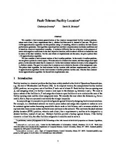
35% 65% 90% 94% 20% 350% 0% 40% 575% 0% 684% 0% 70% 80% 997% 0 % 1100% 00% P e r c e n t a g e o f trFault ip lic aMasking te d h a r d w(%) a r e r e s o u r c e s (F r ) Maximum Operation Frequency (Timing-Aware P&R [1, 2]) Maximum Operation Frequency (Reliability-Aware P&R) Power Consumption (Timing-Aware P&R [1, 2]) Power Consumption (Reliability-Aware P&R) 115% 0%
Fig. 6.
Fault masking under different redundancy scenarios.
injected upsets ranges between 3% and 5% of the size of configuration file, while for a given resource, the temporal distribution between consecutive upsets follows TDDB model [7]. Note that this claim does not affect the generality of the proposed solution. Fig. 6 evaluates the efficiency of proposed framework to mask upsets, as we gradually alleviate the aggressive of redundancy. Horizontal axis corresponds to the percentage of masked over the injected upsets, whereas the maximum operation frequency and power consumption are plotted at left and right vertical axes, respectively. For demonstration purposes, both axes are plotted in normalized manner over the corresponding maximum values among the alternative solutions. For the scopes of this analysis, JPEG application was mapped with two different scenarios: a timing-aware [5] and the proposed reliability-aware frameworks, whereas as reference we employ two border solutions: without fault tolerance (marked as “No TMR”) and with uniform insertion of redundancy (mentioned as “Full TMR”) [1]. A number of conclusions might be derived from Fig. 6. Among others, uniform insertion of redundancy, as it is applied with Xilinx TMR [1], leads to an excessive mitigation cost, which usually is not affordable for consumer products. More specifically, “Uniform TMR” solution imposes a penalty in delay compared to initial application implementation (i.e. without fault masking) ranging between 16% and 25%, depending on the selected framework. Similarly, the penalty in term of power consumption for this instantiation of TMR ranges from 39% (for our proposed reliability-aware framework) up to 78% (regarding the conventional timing-aware P&R). On the other hand, our proposed methodology provides a spectrum of solutions that balance the desired fault masking with the consequence mitigation cost. For instance, assuming that a system can afford reduction at maximum operation frequency up to 5%, then a number of alternative implemen-
Cost = Crit(i, j) × Delay(n)+
�
Maximum affordable degradation in operation frequency
00.65 .6 5
∀i,j∈netlist
�
0 .8 0 0.60
00.70 .7 0
i z(i) × (bbx (i) + bby (i))
i=1
Ctiming =
0 .8 5 0.70
00.80 .8 0
i [z(i) × (bbx (i) + bby (i))] × Act(i) (5)
i=1
Cwire =
0 .9 0 0.80
13% No TMR
Creliability =
N ets h X
0 .9 5 0.90
8%
00.90 .9 0
where
22%
Uniform TMR [1]
h
1.00 1 .0 0
5%
NNormalized o r m a liz e d PPower o w e r CConsumption o n s u m p t io n
N o r m a liz e d M a x im u m O p e r a tio n F r e q u e n c y Normalized Maximum Operation Frequency
11.00 .0 0
Cost =
(8)
� i 1 − Act(i) × bc(n) × hc(n) × pc(n)
, where Delay(n) is the Elmore delay of node n [9], the cap(n) gives the capacity of this node, while bc(n), hc(n) and pc(n) gives the base cost, the historical cost and the present congestion of node n, respectively. V. E XPERIMENTAL R ESULTS This section provides a number of experimental results that prove the efficiency of proposed methodology. For evaluation purposes, we employ a number of industrial oriented kernels [4], whereas the target device is an Altera Stratix-based FPGA without dedicated fault tolerant mechanism. The number of
51
2012 NASA/ESA Conference on Adaptive Hardware and Systems (AHS-2012) tations are feasible, each of which corresponds to different efficiency in fault masking. More specifically, in case we employ our proposed reliability-aware framework, then it is feasible to achieve 68% coverage at upsets due to reliability degradation (this solution is marked with a green color circle in Fig. 6). Similarly, in order to achieve this level of fault coverage with the usage of a timing-aware toolflow [5], then there will be an additional delay about 8%. Furthermore, in case we apply the timing-aware framework and the maximum affordable performance degradation is up to 5%, then our framework reports that only 24% of the injected upsets could be masked (blue color circle in Fig. 6). Note that apart from performance improvement, our proposed reliabilityaware framework achieves also power savings as compared to the existing timing-aware P&R [2]. More specifically, regarding the studied scenario of fault coverage, our solution leads to additional power savings 13%. Next, we evaluate the delay and power penalties, whenever applications are implemented with three alternative frameworks. More specifically, we provide results about a timingaware P&R [5], a power-aware framework [10], as well as the proposed reliability-aware solution. For each of these flows, we study three alternative fault tolerant scenarios: (i) without TMR, (ii) with the proposed ”Compact TMR”, and (iii) uniform insertion of TMR (similar to [1]). For this study we assume (without affecting the generality of proposed methodology) that the selected level of fault coverage (horizontal axis in Fig. 6) is set to 90% of the injected upsets. The results from this analysis are summarized in Tables I and II, respectively. Based on the results summarized in Table I, uniform insertion of redundancy leads to the maximum performance degradation among the studied solutions. More specifically, this approach imposes an average delay overhead, as compared to application implementation without fault tolerance (“No TMR”), ranging from 25% up to 33%, depending on the selected implementation flow. On the other hand, the proposed “Compact TMR” flow introduce significant lower average delay overhead, which ranges between 17% (reliability-aware) and 19% (timing-aware). Apart from the performance improvement, the selectively insertion of TMR results also to considerable power savings. Based on Table II, the power overheads imposed by the uniform insertion of TMR range between 161% and 172%, as compared to initial application implementation (without TMR). On the other hand, the power overhead whenever only critical for failure resources are triplicated (proposed solution), ranges from 49% up to 57%, respectively. Moreover, we have to notice that power savings reported in this table are complementary to those already depicted about maximum operation frequency. Additionally, even though the power-aware toolflow [10] exhibits lower delay and power consumption compared to our proposed reliability-aware framework, it does not tackle issues related to aging phenomena (e.g. thermal stress, temperature gradient, etc). In order to prove this claim, Table III gives the percentage of fault masking, when application implementation
is performed with the three studied toolsets (timing-aware, power-aware and the proposed fault reliability-aware). For this study, the number of injected upsets was set equals to the 5% of the applications configuration file size. Note that such a percentage could be though as a worst-case scenario about the reliability degradation for consumer products [20] [3]. TABLE III P ERCENTAGE OF FAULT MASKING FOR ALTERNATIVE FRAMEWORKS .
Kernel jpeg fip_risc8 aes_core des_des3perf huffman_video oc_mem_ctrl oc_mips oc_wb_dma oc_correlator fm_receiver Average: Improvement:
Timing aware [5] 90.12% 77.20% 83.29% 75.45% 83.23% 87.54% 92.11% 80.98% 85.33% 91.68% 84.95% 1.00
Power aware [10] 79.05% 77.35% 87.40% 88.35% 85.00% 82.82% 81.19% 97.23% 98.19% 85.44% 86.19% 1.01×
Reliability aware 93.01% 91.29% 95.29% 94.19% 98.55% 92.64% 99.01% 98.35% 99.12% 96.45% 95.79% 1.13×
Based on the experimental results summarized in this table, we can conclude that almost 96% of the injected upsets could be successfully masked with our introduced framework, whereas the corresponding percentage for existing solutions, either timing-aware or power-aware, is about 85%. The additional improvement of fault masking could be explained if we take into consideration that upsets at FPGAs are most likely to affect logic resources (CLBs), rather than routing paths, since the number of programmable transistors at utilized logic blocks is considerable higher compared to the corresponding value for utilized routing fabric [21] [22]. Notice that only a subset of fabricated routing resources are actually utilized at designs; hence the majority of corresponding configuration bits remain empty. VI. C ONCLUSION A novel framework for supporting efficient application mapping under reliability constraints, was introduced. Rather than similar approaches that protect the entire design, our solution provides a trade-off between the desired fault coverage and the consequence delay and power overheads. Experimental results proven the efficiency of introduced framework, since it outperforms similar solutions for comparable fault masking. R EFERENCES [1] TMRTool User Guide Xilinx User Guide UG 156, 2004. [2] K. Siozios, and D. Soudris, “A Methodology for Alleviating the Performance Degradation of TMR Solutions,” IEEE Embedded Systems Letters, Vol. 2, No. 4, pp. 111-114, Dec. 2010. [3] J. Srinivasan, et.al., “The impact of technology scaling on lifetime reliability, Proc. of the 2004 Int. Conf. on Dependable Systems and Networks, pp. 177, 2004. [4] Benchmark Designs For The Quartus University Interface Program (QUIP), Version 1.0, Altera Corp., June 2005. [5] V. Betz, J. Rose, and A. Marquardt, “Architecture and CAD for DeepSubmicron FPGAs,” Kluwer Academic Publishers, Feb. 1999. [6] http://proteas.microlab.ntua.gr
52
2012 NASA/ESA Conference on Adaptive Hardware and Systems (AHS-2012) TABLE I E VALUATION
Kernel jpeg fip_risc8 aes_core des_des3perf huffman_video oc_mem_ctrl oc_mips oc_wb_dma oc_correlator fm_receiver Average: Overhead: Total penalty:
IN TERM OF MAXIMUM OPERATION FREQUENCY
Timing-aware P&R No Compact Uniform TMR TMR TMR 73.36 61.37 60.68 49.06 43.17 39.15 108.67 98.89 89.81 90.24 81.21 69.73 162.28 129.83 110.35 86.92 73.88 76.80 24.3 21.63 20.08 91.8 74.36 80.24 51.02 39.90 43.18 42.5 32.06 35.19 78.02 65.63 62.52 18.87% 24.78% 18.87% 24.79%
(MH Z ).
Power-aware P&R No Compact Uniform TMR TMR TMR 68.96 59.42 50.62 46.6 38.22 33.36 103.23 85.68 86.93 83.02 74.72 66.78 154.17 124.27 104.29 81.7 71.90 64.32 23.09 20.08 17.74 87.21 74.13 59.67 46.94 41.04 38.77 39.10 31.88 33.58 73.40 62.13 55.61 18.13% 32.00% 6.29% 25.57% 40.28%
Reliability-aware P&R No Compact Uniform TMR TMR TMR 60.68 49.76 45.51 41.01 36.09 28.71 98.89 81.73 79.85 81.21 66.33 63.99 129.83 120.65 99.61 73.88 64.69 53.31 21.63 18.46 15.68 74.36 60.00 53.25 39.79 33.91 29.02 33.63 29.25 23.76 65.49 56.09 49.27 16.77% 32.92% 19.13% 39.09% 58.35%
TABLE II E VALUATION
Kernel jpeg fip_risc8 aes_core des_des3perf huffman_video oc_mem_ctrl oc_mips oc_wb_dma oc_correlator fm_receiver Average: Overhead: Total penalty:
IN TERM OF POWER CONSUMPTION ( M WATT ).
Timing-aware P&R No Compact Uniform TMR TMR TMR 190.00 283.10 507.30 98.00 141.12 263.62 127.00 181.61 335.28 447.00 733.08 1166.67 218.00 368.42 647.46 193.00 306.87 482.50 56.00 74.48 166.88 229.00 384.72 638.91 119.00 176.12 354.62 95.00 137.75 264.10 177.20 278.73 482.73 57% 172% 57% 172%
Power-aware P&R No Compact Uniform TMR TMR TMR 171.00 212.33 410.91 75.46 118.54 229.35 109.22 143.47 281.64 393.36 608.46 898.34 183.12 287.37 582.71 167.91 248.56 361.88 44.80 62.56 133.50 206.10 327.01 562.24 96.39 153.22 273.06 76.00 114.33 235.05 152.34 227.59 396.87 49% 161% -14.02% 28.43% 124%
[7] R. Doering and Y. Nishi, “Handbook of semiconductor manufacturing technology,” 2nd Edition, CRC Press, Taylor & Francis Group, 2008. [8] Marquardt, A., Betz, V., and Rose, J., Timing-Driven Placement for FPGAs, Proc. Intl. Symp. on FPGAs, pp. 203-213, Feb. 2000. [9] L. McMurchie and C. Ebeling, “PathFinder: a negotiation-based performance-driven router for FPGAs,” Proc. of the ACM Int. Symp. on Field-Programmable Gate Arrays, Feb. 1995, pp. 111-117, 1995. [10] J. Lamoureux and S. Wilton, “On the Interaction Between PowerAware Computer-Aided Design Algorithms for Field-Programmable Gate Arrays”, Journal of Low Power Electronics, Vol.1, No.2, August 2005, pp. 119-132. [11] S. Borkar, “Design challenges of technology scalling”, IEEE Micro, pp. 23-29, July-Aug. 1999. [12] Lesea, et. al., , “Powering Xilinx FPGAs”, 2002 [13] W. Huang, et.al., ”Accurate, Pre-RTL Temperature-Aware Processor Design Using a Parameterized, Geometric Thermal Model”, IEEE Trans. on Computers, 57(9):1277-88, Sept. 2008. [14] R. Jain, A. Mukherjee and K. Paul, ”Defect-aware design paradigm for reconfigurable architectures”, IEEE Computer Society Annual Symposium on Emerging VLSI Technologies and Architectures, 2006. [15] S. Sivaswamy and K. Bazargan, ”Statistical analysis and process variation-aware routing and skew assignment for fpgas”, ACM Trans. Reconfigurable Technol. Syst. Vol. 1, No. 1, pp. 135, 2008. [16] R. Rubin, et.al,”Choose-your-own-adventure routing: lightweight loadtime defect avoidance”, Int. Symp. on FPGAs, pp. 23-32, 2009. [17] K. Nikolic, A, Sadek, and M. Forshaw, “Fault-tolerant techniques for nanocomputers”, Nanotechnology 13, pp. 357362, 2002. [18] D. Bhaduri, and S. Shukla, “NANOPRISM: A Tool for Evaluating Granularity vs. Reliability Trade-offs in Nano Architectures”, Great Lakes Symposium on VLSI (GLSVLSI), pp. 109-112, 2004.
Reliability-aware P&R No Compact Uniform TMR TMR TMR 172.90 260.45 466.72 90.16 132.65 242.53 120.65 168.90 318.52 424.65 659.77 998.41 202.74 350.00 615.09 177.56 276.18 434.25 52.64 67.78 153.53 208.39 365.48 594.19 111.86 165.55 326.25 90.25 129.49 240.33 165.18 257.63 438.98 56% 166% -6.78% 45.37% 148%
[19] F. Kastensmidt, L. Carro, and R. Reis,“Fault-Tolerance Techniques for SRAM-Based FPGAs”, Springer, 2006. [20] ITRS, “International technology roadmap for semiconductors, yield enhancement”, Tech. Rep., 2009. [21] Altera, “Stratix device handbook”, Jul 2005. [22] V. Kalenteridis, H. Pournara, K. Siozos, K. Tatas, N. Vassiliadis, I. Pappas, G. Koutroumpezis, S. Nikolaidis, S. Siskos, D. Soudris, and A. Thanailakis, “A complete platform and toolset for system implementation on fine-grain reconfigurable hardware”, Microprocessors and Microsystems, vol. 29, no. 6, pp. 247259, 2005. [23] S. Mahapatra, M. A. Alam, P. B. Kumar, T. R. Dalei, D. Varghese, and D. Saha, “Negative bias temperature instability in cmos devices”, Microelectron. Eng., vol. 80, pp. 114121, June 2005 [24] W. Huang, S. Ghosh, S. Velusamy, K. Sankaranarayanan, K. Skadron, and M. Stan, “Hotspot: a compact thermal modeling methodology for early-stage vlsi design”, Very Large Scale Integration (VLSI) Systems, IEEE Transactions on, vol. 14, no. 5, pp. 501513, may 2006. [25] K. Siozios, D. Rodopoulos, and D. Soudris, “On supporting rapid thermal analysis”, IEEE Computer Architecture Letters, vol. 99, no. RapidPosts, 2011.
53