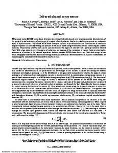
270
IEEE TRANSACTIONS ON MICROWAVE THEORY AND TECHNIQUES, VOL. 56, NO. 2, FEBRUARY 2008
A Monolithic Phased Array Using 3-bit Distributed RF MEMS Phase Shifters Kagan Topalli, Student Member, IEEE, Özlem Aydin Civi, Senior Member, IEEE, Simsek Demir, Member, IEEE, Sencer Koc, and Tayfun Akin, Member, IEEE
Abstract—This paper presents a novel electronically scanning phased-array antenna with 128 switches monolithically implemented using RF microelectromechanical systems (MEMS) technology. The structure, which is designed at 15 GHz, consists of four linearly placed microstrip patch antennas, 3-bit distributed RF MEMS low-loss phase shifters, and a corporate feed network. metal–air–metal capacitors are MEMS switches and highemployed as loading elements in the phase shifter. The system is fabricated monolithically using an in-house surface micromachining process on a glass substrate and occupies an area of 6 cm 5 cm. The measurement results show that the phase shifter can provide nearly 20 /50 /95 phase shifts and their combinations at the expense of 1.5-dB average insertion loss at 15 GHz for eight combinations. It is also shown by measurements that the main beam can be steered to required directions by suitable settings of the RF MEMS phase shifters. Index Terms—Microelectromechanical systems (MEMS), micromachining, microwave, phased array, phase shifter.
I. INTRODUCTION
O
VER THE past decade, RF microelectromechanical systems (MEMS) technology has offered solutions for the implementation of novel components and systems [1], [2]. This technology promises to solve many limitations of other technologies, especially for high-frequency applications. RF MEMS enables the realization of reconfigurable components such as switches, capacitors, and phase shifters with low insertion loss, low power consumption, and high linearity compared to the conventional techniques. One of the important components of the RF MEMS technology is to implement RF MEMS phase shifters for phased-array applications that require better performance than the arrays with conventional phase shifters in terms of losses and size. Phased arrays consist of multiple stationary radiating elements each of which are fed by tunable phase or time-delay control units to steer the beam [3], [4]. Phased arrays are generally implemented using separately produced components such as a feed network, phase shifters, and antennas. Hybrid connection
of these components not only increases the system size, but also introduces parasitic effects, packaging cost, and losses. In order to eliminate these drawbacks, there is a need to produce these components on the same substrate, forming a monolithic phased array, which is possible with the enabling RF MEMS technology [5], [6]. This paper presents a novel monolithic electronically scanning array using the RF MEMS technology. The phased-array system in this study is designed to operate at 15 GHz, and it employs 3-bit distributed MEMS transmission line (DMTL) type phase shifters. These phase shifters are monolithically integrated with the feed network and four linearly placed microstrip patch antennas on the same substrate [6]. The use of MEMS phase shifters in a phased array offers some advantages. First, MEMS phase shifters have low-loss performance with nearly zero dc power consumption compared to semiconductor-based counterparts [7], [8]. Moreover, MEMS phase shifters are suitable for monolithic phased-array designs with their reduced cost and volume compared to semiconductor- and ferrite-based counterparts. The phase shifters in the phased array presented in this study are used to obtain various combinations of progressive phase shift in the excitation of radiating elements to steer the beam. In this study, phase-shifter performance is improved using high- metal–air–metal (MAM) capacitors in addition to MEMS switches. Furthermore, the system losses and size are reduced by implementing the RF MEMS phase shifters in a phased array monolithically manufactured by micromachining technology. To the authors’ knowledge, this study is one of the first few monolithically fabricated electronically scanning phased-array systems employing a large amount of RF MEMS components reported in the literature [5], [6]. Section II gives the configuration of the electronically scanning array, while Section III presents the design, implementation, and measurement results of the low-loss MEMS phase shifter used in the phased array. Section IV provides the fabrication and measurement results of the array, which is followed by conclusions in Section V. II. PHASED-ARRAY STRUCTURE
Manuscript received April 26, 2007; revised October 4, 2007. This work was supported by The Scientific and Technical Research Council of Turkey (TUBITAK-EEEAG-104E041), by the Turkish State Planning Organization (DPT), and by the AMICOM (Advanced MEMS For RF and Millimeter Wave Communications) Network of Excellence under the 6th Framework Program of the European Union. The authors are with the Department of Electrical and Electronics Engineering, Middle East Technical University, Ankara 06531, Turkey (e-mail:
[email protected]). Color versions of one or more of the figures in this paper are available online at http://ieeexplore.ieee.org. Digital Object Identifier 10.1109/TMTT.2007.914377
The phased array proposed in this paper is composed of four microstrip patch antennas, a corporate feed network, and four RF MEMS phase shifters. The operation frequency is selected as 15 GHz to be able fit the entire system into a single . 500- m-thick 4-in glass substrate The total size of the system is approximately 6 cm 5 cm. The device is fabricated using the surface micromachining process developed at the Middle East Technical University (METU), Ankara, Turkey. Fig. 1 presents a layout and photograph of
0018-9480/$25.00 © 2008 IEEE
TOPALLI et al.: MONOLITHIC PHASED ARRAY USING 3-bit DISTRIBUTED RF MEMS PHASE SHIFTERS
271
Progressive phase shifts of 135 and 180 can also be provided by the phase shifter; however, the main beam cannot be steered to the corresponding scan angles due to the element pattern. III. DIGITAL PHASE SHIFTER USING MAM CAPACITORS
Fig. 1. Proposed monolithically integrated phased array. (a) Layout drawing and (b) photograph of the fabricated device. The device is fabricated using an in-house surface micromachining process. The total chip size is approximately 6 cm 5 cm.
2
the monolithically integrated phased array. Microstrip patch antennas having dimensions of 4.65 mm 4.65 mm are equally spaced by (1 cm) distance from each other’s phase center. A corporate feed network, which is composed of 70 (2.2 mm) transformers, is optimized at around 15 GHz. The width of 50- and 70- lines are 0.95 and 0.43 mm. Tapered lines with low return loss are required for the transitions from microstrip lines to conductor backed coplanar waveguide (CB-CPW) since RF MEMS phase shifters are implemented on CB-CPW. These phase shifters are designed to provide progressive phase shifts of 45 /90 /180 and their combinations at 15 GHz. When both the array factor and element pattern are taken into account, the 3-dB beamwidth of the array is 25 , and the main beam can be rotated to approximately 12 and 24 for progressive phase shifts of 45 and 90 , respectively.
Most phase shifters currently being used in phased arrays are based on ferrite or semiconductor devices such as p-i-n diodes or field-effect transistor (FET) switches. Ferrite-based phase shifters are generally used in arrays where a low insertion loss is required ( 1 dB) and slow-switching time (150 s) is permissible [9], [10]. However, these phase shifters are not suitable for the implementation of low-profile and low-weight phased arrays. FET-based phase shifters consume very low power, but they have a large amount of RF loss (4–6 dB at 12–18 GHz) [11]. p-i-n diode-based phase shifters consume more dc power and have slightly better performance compared to FET-based phase shifters [12], [13]. However, the semiconductor device-based phase shifter cannot compete with the loss performance of the MEMS-based phase shifter, which has been shown with various designs [1]. MEMS phase shifters are designed using switched line [7], [8] or distributed loaded line [14]–[19] approaches. Switched line phase shifters are implemented using MEMS switches on microstrip transmission lines. These phase shifters either require via-holes for series switch configuration, increasing the fabrication complexity [7], or radial stubs for shunt switch configuration, limiting the bandwidth of the phase shifter [8]. Among the MEMS phase shifters, the ones designed using distributed techniques, namely, DMTL, offer wideband and low-loss cascadable devices with a simple design and fabrication method on relatively and glass low-permittivity substrates such as quartz . These low-permittivity substrates also allow the implementation of radiators monolithically integrated with the phase shifters. Therefore, the monolithic phased-array structure in this study employs a phase-shifter structure designed using distributed techniques. The reason for low-loss characteristics of a MEMS phase shifter is that the MEMS switches used in the implementation of a DMTL have a very low series resistance (0.1–0.3 ) compared to solid-state devices [14]–[19]. The average loss of a typical 3-bit MEMS phase shifter is 1.2 dB at 13.6 GHz [17], which is a 3–4-dB improvement compared to designs using GaAs FET switches. This leads to an improvement of 6–8 dB in the insertion loss of a radar system. Therefore, one of the amplifier stages can be removed from the system, reducing both dc power consumption and manufacturing costs of the system. A. Phase-Shifter Design The digital phase shifter used in the system is composed of a periodically loaded high-impedance transmission line with MEMS bridges in series with lumped capacitors forming a DMTL [15]. Fig. 2 shows a general view of the phase shifter and its unit cell. Fig. 3 gives the corresponding circuit model of the unit cell, which provides the required closed-form expressions. The unit cell has two states for the bridge: the up position and the down position. The total loading capacitance when the MEMS bridge is in the upstate position is the series and . As the bridge is combination of two capacitors:
272
IEEE TRANSACTIONS ON MICROWAVE THEORY AND TECHNIQUES, VOL. 56, NO. 2, FEBRUARY 2008
electric constant of the unloaded transmission line, respectively. The periodicity, i.e., the total length of the unit cell, is defined as , and it is optimized as 800 m considering the Bragg frequency, , which is the cutoff frequency observed in periodic structures when the guided wavelength is getting closer to the GHz as periodic spacing. The selection of ( GHz) ensures the proper operation of the phase shifter as true-time delay at 15 GHz with acceptable return and insertion losses. The following equations can be solved to define the required capacitance values and periodicity. Equations (1)–(4) are based on the work of Hayden and Rebeiz [17] and Hung et al. [18], and are summarized here for completeness: meters farads
(3) farads
Fig. 2. (a) Phase-shifter structure. The air bridge on the external resistor is removed in the drawing for better visualization. (b) Top view of the unit cell of the phase shifter showing the dimension.
Fig. 3. Circuit model for the unit cell of the phase shifter.
actuated by applying a dc-bias voltage and collapsed on the dc isolation dielectric, the bridge capacitance increases by a factor of 60–70 theoretically, and the resulting loading capacitance seen by the line is simply reduced to . These two states in the loading capacitance yields two distinct loaded characteris(upstate loaded charactics impedance of DMTL, namely, (downstate loaded characterteristic impedance: 58 ) and istic impedance: 44 ), where an acceptable return loss for both states can be achieved [17]–[19]. The phase shift per unit section can be controlled with the change of the phase velocity due to the change in the loaded characteristic impedance as [17]:
(2)
(4)
The designed unit cell shown in Fig. 2(b) can provide nearly an 11.5 phase shift at 15 GHz, which is verified with Ansoft’s High Frequency Structure Simulator (HFSS) simulations where (55 fF) and (115 fF) are tuned to achieve the specified and . The nonmovable static capacitor is realized as a MAM capacitor, which has a high- factor ( 400 at 15 GHz) compared to metal–insulator–metal (MIM) capacitors [17]. The height of membranes in the MAM capacitor and the switch is 2 m. The characteristic impedance of the unloaded transmission line is selected to be (CB-CPW dimensions: m, m). The attenuation constant and of the unloaded line is found the effective dielectric constant to be 20 dB/m and 2.8 at 15 GHz, respectively [20]. The overall 3-bit RF MEMS phase shifter employed in the system consists of three sections with a total of 28 unit cells within an area of 22.4 mm 2.1 mm. The first section has four . The cells and is designed to have a phase shift of second section has eight cells providing 90.4 , and the next 16 cells forms the third bit, which is designed to give 182.6 at 15 GHz. The dominant loss mechanism of the phase shifter is the loss of the unloaded CB-CPW. However, the series resistance of the also play a significant role. bridge and the factor of the To be more specific, in order to accurately model the loss of in the upstate the structure, a series resistance of and in the downstate is used, which is found by is found curve fitting. The factor of the static capacitor k . The high- values to be 433 with a value of of MAM capacitors improve the loss performance of the phase shifter. However, the bias resistors have an adverse effect on the factor of the capacitors and the loss of the phase shifter, which is explained in Section III-B. B. Effect of Bias Resistors
rad/section
(1)
where is the frequency in radians, is the free-space velocity, and and is the characteristic impedance and effective di-
In order to actuate each section of the phase shifter separately, thin-film resistors are employed. Fig. 2(b) shows that Si–Cr bias lines are placed inside the gaps of CB-CPW extending from one bridge to the other to carry the dc actuation voltage. The con-
TOPALLI et al.: MONOLITHIC PHASED ARRAY USING 3-bit DISTRIBUTED RF MEMS PHASE SHIFTERS
273
TABLE I SIMULATED AND MEASURED CIRCUIT PARAMETERS FOR THE UNIT CELL OF THE DMTL PHASE SHIFTER
Fig. 4. Simulated insertion loss of the phase shifter, which is obtained from S when the ports of the structure are tuned as 44 (Z ).
ductivity of the Si–Cr layer is optimized during the fabrication S/m), which is cruprocess to have a low value ( Si Cr cial in determining the loss of the structure. The return loss of the structure is not significantly affected by the presence of the bias resistors since the return loss is determined by the loaded and , which are only affected from the line impedances unloaded transmission line parameters and the loading capaciand . Fig. 4 shows the effect of the bias lines using tors the simulation results of insertion-loss characteristics. The designed phase shifter has an insertion loss of nearly 1.08 dB for the worst case (i.e., when all switches are down) if no bias lines are present. The insertion loss is calculated directly from characteristics with the return loss removed by tuning the port impedance to 44 , i.e., downstate loaded line impedance. The bias lines, which are placed inside the gaps of the CB-CPW, have an adverse effect on the insertion loss due to the decrease of the factor of the static capacitor . The internal Si–Cr bias lines of shown in Fig. 3 are shunt connected to the self resistance the static capacitor , reducing the factor. Since each static capacitor sees two bias lines, the equivalent resistance of the careduces to from (40 k ) where pacitor (internal bias resistor) is equal to 20 k S/m, Si–Cr m, width m, and thickness m). length The factor reduces accordingly to 87 from 433. The insertion loss of the entire structure, which is calculated as 1.08 dB without any bias lines, increases to 1.56 dB due to reduced factor of . The external bias resistors that are placed underneath the air bridges on the ground depicted in Fig. 2 are used only for the three cells to actuate each bit separately. Due to the strong coupling between the ground plane and external bias resistor underneath, the external bias resistor is modeled with k . The factor a smaller effective resistance of the static capacitor reduces accordingly to 13 for those three cells. The insertion loss of the structure is 1.91 dB, where the factor of three cells with external bias lines is 13 and the factor of the remaining 25 cells (out of 28) is 87. C. Phase-Shifter Measurements The phase shifters of the phased array are also fabricated separately on the same wafer for characterization purposes. They are measured using thru-reflect-line (TRL) calibration with a
port impedance of 77 , where all eight states are measured by applying dc voltage with dc probes and bias tee. Actuation voltage of the phase shifters is measured to be 16 V. All the states have a return loss better than 10 dB with a worst case insertion loss of 2 dB at 15 GHz. The average insertion loss for eight states is 1.5 dB. Table I shows the simulated and measured circuit parameters for the unit cell. The bridge capacitance for ) can be fabricated very close to the designed the upstate ( value. However, the MAM capacitors ( ) show a deviation compared to the simulated value. The measured downstate capacitance value is also degraded compared to simulated value due to the surface roughness [21]. Nevertheless, the measured downstate capacitance is high enough to have a virtual short circuit through the bridge. The MAM capacitors have a different mechanical design and are fixed on three sides to have a rigid structure that might result in an increase in the height due to the residual stress on the structural layer metal. Fig. 5 shows a 3-D plot of the surface profile data of the fabricated phase shifter obtained using a light-interferometer microscope. The bridge height is around 2 and 2.6 m for the central bridge and MAM capacitor, respectively. The decrease of the MAM capacitances and . The shift reduces shifts the loaded line impedances unit cell performance of the measured phase shifter to 6 according to (1), which is 11 for the designed phase shifter. Fig. 6 shows the measured insertion phase characteristics for all the states of the phase shifter. The measured phase shifter provides approximately 20 /50 /95 phase shifts and their combinations. Table II shows simulated and measured loss components at 15 GHz. The loaded line loss, which is defined when , is directly related to the unloaded . The loaded line line loss with a multiplicative factor of loss is increased in the measurements due to the increase of the of the unloaded line. The factor attenuation constant losses are increased not only due to the decrease of the quality factor, but also due to the change of the loaded line impedance factor of to 52.9 from the designed value of 44 . The the MAM capacitors with internal bias resistors reduces to 53
274
IEEE TRANSACTIONS ON MICROWAVE THEORY AND TECHNIQUES, VOL. 56, NO. 2, FEBRUARY 2008
Fig. 5. Surface profiler view of the unit cell of the phase shifter obtained using an interferometer microscope.
Fig. 7. Insertion loss of the phase shifter (extracted from measurement results), which is obtained from S when the ports of the structure are tuned as 52:9 (Z ).
Fig. 6. Measured insertion phase-shift characteristics of the phase shifter for different states.
TABLE II SIMULATED AND MEASURED LOSS COMPONENTS AT 15 GHz. LOADED LINE LOSS IS DEFINED WHEN R = 0 ; R = 40 k ; R = R
!1
(simulated value: 87) due to the decrease of the capacitance factor of the MAM capacitors having both invalue. The ternal and external resistors is equal to 8 (simulated value: 13). Fig. 7 shows the insertion-loss analysis for the measured structure illustrating the effect of -factor values of MAM capaci(no bias line present) for 28 tors. These cases are: 1) cells; 2) for 28 cells; and 3) (for 25 cells) (for three cells). The analysis also shows that if a and conductivity of 2500 S/m is achieved, the worst case insertion factors loss can be reduced down to nearly 1.6 dB, where can be increased to 132 for 25 cells with internal bias resistors and to 22 for three cells with both internal and external resistors. The average insertion loss of the phase shifter would be approximately 1.3 dB, which is quite close to the reported losses of these types of MEMS phase shifters [17]. The conductivity
Fig. 8. Process flow used in the fabrication of the phased array.
value of the Si–Cr film depends on the chamber conditions of the sputter equipment and the gas flow during processing, and it can be reduced by process optimizations to further reduce the losses of the phase shifters, which is under progress.
TOPALLI et al.: MONOLITHIC PHASED ARRAY USING 3-bit DISTRIBUTED RF MEMS PHASE SHIFTERS
275
Fig. 10. Measured return loss of the monolithic phased array.
Fig. 9. SEM photographs of the phase-shifter structure. (a) Two unit cells where Si–Cr internal resistors connecting the unit cells to carry dc signal can be seen. (b) Detailed view of the anchor region of the MEMS bridge where both external and internal resistors are attached. Etch holes on the suspended regions are used to improve the removal of sacrificial layer underneath those regions.
IV. FABRICATION AND MEASUREMENTS OF THE ARRAY The phased array presented in this study is fabricated using the surface micromachining process developed at METU for implementation of various RF MEMS components on 500- m-thick Pyrex 7740 glass substrates . The backside of the wafer is coated with a 100-Å/2- m Ti/Au layer by sputtering for ground metallization of microstrips and CB-CPWs. Fig. 8(i)–(vi) shows the surface micromachining process. (i) The process begins with 2000-Å-thick Si-Cr resistive layer deposition by sputtering and patterning by wet etching. (ii) The next step is the sputtering of a 100/3000-Å-thick Ti/Au layer, which is required as the seed layer for electroplating of the base metallization. The base metallization layer is formed using a 2- m-thick gold layer, which is electroplated inside the regions defined by the mold photoresist. The remaining Ti/Au seed layer is etched using wet etching with selective titanium and gold etchants. (iii)
Fig. 11. Measured radiation pattern of the monolithic phased array for different progressive phase shifts.
A 3000-Å-thick Si N layer is coated as the dc isolation layer using a plasma enhanced chemical vapor deposition technique (PECVD) and patterned using the reactive ion etching (RIE) technique. (iv) The next step is the spin coating of the photodefinable polyimide (PI 2737) as the 2- m-thick sacrificial layer. (v) A 1- m-thick gold layer is then sputter deposited and patterned as the structural layer. (vi) The sacrificial layer photoresist stripper, rinsed in is wet etched in the isopropyl alcohol, and dried in a supercritical point dryer. Fig. 9 shows the scanning electron microscrope (SEM) photographs of the phase shifters fabricated using the process flow described above. The radiation pattern measurements of the phased array are performed via an in-house anechoic chamber. In order to apply the dc voltages, the fabricated phased array is attached to a printed circuit board (PCB) card. There exist mechanical switches located at the back of the card in order not to affect the radiation characteristics. The dc connections to the phased array are obtained using wire bonds. Fig. 10 shows the reflection coefficient characteristics of the phased array. The measured resonant frequency of the system is at 14.62 GHz with a 10-dB
276
IEEE TRANSACTIONS ON MICROWAVE THEORY AND TECHNIQUES, VOL. 56, NO. 2, FEBRUARY 2008
bandwidth of 6%, which is very close to the designed value of 15 GHz with a 10-dB bandwidth of 2.5% [6]. Fig. 11 gives the measured radiation patterns of the phased array for different phase-shifter settings. It is observed that the beam can be tilted by 4 and 14 when the progressive phase shifts are adjusted nearly 20 and 50 , respectively. These values are quite close to the expected amount of steering. The back-radiation levels around 15 dB are acceptable considering the PCB card and the mechanical switches attached to this card for dc biasing of MEMS phase shifters. V. CONCLUSION This paper has presented the design and implementation of a novel monolithic phased-array system with RF MEMS phase shifters. The phased-array system is fabricated using the micromachining process developed at METU. The system employs 3-bit DMTL-type RF MEMS phase shifters, which are composed of high-impedance transmission lines loaded with MEMS bridges in series with MAM capacitors. The phase shifter can provide nearly 20 /50 /95 phase shifts and their combinations at the expense of 1.5-dB average insertion loss at 15 GHz, showing low-loss performance compared to semiconductor counterparts. The reduction of the losses in the phase-shifting elements of a phased array can be used to eliminate one of the amplification stages, decreasing both the system costs and dc power consumption. Radiation pattern measurements shows that the beam can be steered to the desired angles by the appropriate settings of MEMS phase shifters. This study shows that the use of RF MEMS phase shifters monolithically integrated with patch antennas and feed network can offer better performance phased arrays by reducing the dc power consumption, packaging costs, and the size of the system compared to arrays with ferrite- or semiconductor-based phase shifters. This study is one of the first that demonstrate the monolithic implementation of a phased array on a single substrate with an acceptable performance, which can be further improved by increasing the number of antenna elements. Such monolithically integrated MEMS-based phased arrays can be a good candidate in weight- and power-constrained applications such as fire-control radars and automotive radars. ACKNOWLEDGMENT The authors would like to thank to the Microelectronic Technologies staff of the Middle East Technical University, Ankara, Turkey, particularly O. S. Akar, for their support in the fabrication. The authors also thank M. Unlu and H. I. Atasoy for the process development and RF measurements. REFERENCES [1] G. M. Rebeiz, RF MEMS Theory, Design, and Technology. Hoboken, NJ: Wiley, 2003. [2] B. R. Norvell, R. J. Hancock, J. K. Smith, M. I. Pugh, S. W. Theis, and J. Kviakofsky, “Micro electro mechanical switch (MEMS) technology applied to electronically scanned arrays for space based radar,” in Proc. Aerosp. Conf., 1999, pp. 239–247. [3] R. J. Mailloux, Phased Array Antenna Handbook. Norwood, MA: Artech House, 1994.
[4] D. Parker and D. C. Zimmermann, “Phased arrays—Part II: Implementations, applications, and future trends,” IEEE Trans. Microw. Theory Tech., vol. 50, no. 3, pp. 688–698, Mar. 2002. [5] K. Van Caekenberghe, T. Vaha-Heikkila, G. Rebeiz, and K. Sarabandi, -band MEMS TTD passive electronically scanned array (ESA),” “ in IEEE Antennas Propag. Symp. Dig., Jul. 2006, pp. 513–516. [6] K. Topalli, M. Unlu, O. A. Civi, S. Demir, S. Koc, and T. Akin, “A monolithic phased array using 3-bit DMTL RF MEMS phase shifters,” in IEEE Antennas Propag. Symp. Dig., Jul. 2006, pp. 517–520. [7] M. Kim, J. B. Hacker, R. E. Mihailovich, and J. F. DeNatale, “A DC-to-40 GHz four-bit RF MEMS true-time delay network,” IEEE Microw. Wireless Compon. Lett., vol. 11, no. 2, pp. 56–58, Feb. 2001. [8] B. Pillans, S. Eshelman, A. Malczewski, J. Ehmke, and C. Goldsmith, “ -band RF MEMS phase shifters,” IEEE Microw. Guided Wave Lett., vol. 9, no. 12, pp. 520–522, Dec. 1999. [9] W. E. Hord, C. R. Boyd, Jr., and D. Diaz, “A new type of fast switching dual-mode ferrite phase shifter,” in IEEE MTT-S Int. Microw. Symp. Dig., Jun. 1987, vol. II, pp. 985–988. [10] C. R. Boyd, “An accurate analog ferrite phase shifter,” in IEEE MTT-S Int. Microw. Symp. Dig., May 1971, pp. 104–105. [11] V. Sokolov, J. J. Geddes, A. Contolatis, P. E. Bauhahn, and C. Chao, “A -band GaAs monolithic phase shifter,” IEEE Trans. Microw. Theory Tech., vol. MTT-31, no. 12, pp. 1077–1083, Dec. 1983. [12] P. R. Shepherd and M. J. Cryan, “Schottky diodes for analog phase shifters in GaAs MMIC’s,” IEEE Trans. Microw. Theory Tech., vol. 44, no. 11, pp. 2112–2116, Nov. 1996. [13] J. F. White, “Diode phase shifters for array antennas,” IEEE Trans. Microw. Theory Tech. (Special Issue), vol. MTT-22, no. 6, pp. 658–674, Jun. 1974. [14] K. Topalli, M. Unlu, S. Demir, O. A. Civi, S. Koc, and T. Akin, “New approach for modeling distributed MEMS transmission lines,” Proc. Inst. Elect. Eng.—Microw. Antennas Propag., vol. 153, no. 2, pp. 152–162, Apr. 2006. [15] N. S. Barker and G. M. Rebeiz, “Optimization of distributed MEMS transmission-line phase shifters— -band and -band designs,” IEEE Trans. Microw. Theory Tech., vol. 48, no. 11, pp. 1957–1966, Nov. 2000. [16] J. Perruisseau-Carrier, R. Fritschi, P. Crespo-Valero, and A. K. Skrivervik, “Modeling of periodic distributed MEMS, application to the design of variable true-time delay lines,” IEEE Trans. Microw. Theory Tech., vol. 54, no. 1, pp. 383–392, Jan. 2006. [17] J. S. Hayden and G. M. Rebeiz, “Very low-loss distributed -band and -band MEMS phase shifters using metal–air–metal capacitors,” IEEE Trans. Microw. Theory Tech., vol. 51, no. 1, pp. 309–314, Jan. 2003. [18] J.-J. Hung, L. Dussopt, and G. M. Rebeiz, “Distributed 2- and 3-bit -band MEMS phase shifters on glass substrates,” IEEE Trans. Microw. Theory Tech., vol. 52, no. 2, pp. 600–606, Feb. 2004. [19] H. T. Kim, J. H. Park, S. Lee, S. Kim, J. M. Kim, Y. K. Kim, and Y. Kwon, “ -band 2-b and 4-b low-loss and low-voltage distributed MEMS digital phase shifter using metal–air–metal capacitors,” IEEE Trans. Microw. Theory Tech., vol. 50, no. 12, pp. 2918–2923, Dec. 2002. [20] R. N. Simons, Coplanar Waveguide Circuits, Components and Systems. New York: Wiley, 2001. [21] J. B. Muldavin and G. M. Rebeiz, “High isolation CPW MEMS shunt switches—Part I: Modeling,” IEEE Trans. Microw. Theory Tech., vol. 48, no. 6, pp. 1045–1052, Jun. 2000.
Ka
Ka
Ka
U
W
X
Ka
W
V
Kagan Topalli (S’99) was born in Eskisehir, Turkey, in 1979. He received the B.Sc. and Ph.D. degrees in electrical and electronics engineering from the Middle East Technical University (METU), Ankara, Turkey, in 2001 and 2007, respectively. From 2001 to 2007, he was a Research Assistant with the Department of Electrical and Electronics Engineering, METU. He is currently a Senior Research Scientist with the same department. His major research interests include development, characterization, and integration of novel RF MEMS structures such as switches, phase shifters, and impedance tuners for RF front ends at microwave and millimeter wave, reconfigurable antennas, phased arrays, microwave packaging, and microfabrication technologies.
TOPALLI et al.: MONOLITHIC PHASED ARRAY USING 3-bit DISTRIBUTED RF MEMS PHASE SHIFTERS
Özlem Aydin Civi (S’90–M’97–SM’05) received the B.Sc., M.Sc., and Ph.D. degrees in electrical and electronics engineering from the Middle East Technical University (METU), Ankara, Turkey, in 1990, 1992, and 1996, respectively. From 1990 to 1996, she was a Research Assistant with METU. From 1997 to 1998, she was a Visiting Scientist with the ElectroScience Laboratory, The Ohio State University. Since 1998, she has been with the Department of Electrical and Electronics Engineering, METU, where she is currently an Associate Professor. Her research interests include analytical, numerical, and hybrid techniques in electromagnetic theory problems, especially fast asymptotic/hybrid techniques for the analysis of large finite periodic structures, multifunction antenna design, phased arrays, and RF MEMS applications. Since 1997, she has been a national expert on antennas of the European actions COST260, COST284, COST-IC0603. She is one of the work package leaders on RF MEMS of AMICOM, a European Network of Excellence. Since 2004, she has been a Technical Reviewer of the European community for scientific projects in the fields of antennas and communication. She has authored or coauthored over 80 journal and international conference papers. Dr. Civi was chair of the IEEE Antennas and Propagation (AP)/Microwave Theory and Techniques (MTT)/Electron Devices (ED)/Electromagnetic Compatibility (EMC) Chapter from 2004 to 2006. She is the chair of the IEEE Turkey Section and a member of the Administrative Committee of the Turkish National Committee, URSI. She was a recipient of the 1993 Erol Gelenbe Best Masters Thesis Award, the 1994 Prof. Mustafa Parlar Foundation Research and Encouragement Award with the METU Radar Group, and the 1996 URSI Young Scientist Award.
Simsek Demir (S’91–M’98) received the B.Sc., M.Sc., and Ph.D. degrees in electrical and electronics engineering from Middle East Technical University (METU), Ankara, Turkey, in 1991, 1993 and 1998, respectively. From 1991 to 1998, he was a Research Assistant with METU. From 1998 to 1999, he contributed to atmospheric radar antenna design with the International Research Centre for Telecommunications-Transmission and Radar, Technical University of Delft (TU-Delft), Delft, Netherlands. Since 2000, he has been a Professor with the Department of Electrical and Electronics Engineering, METU. His main scientific interests include microwave and millimeter-wave active and passive component and system design, analysis, and modeling. Some of his research topics have been exploitation of RF MEMS technology toward industrial use, power amplifier design, modeling and implementation, and radar applications. Dr. Demir was a recipient of several awards including the North Atlantic Treaty Organization (NATO) A2 Fellowship, which supported him as a Visiting Researcher with the University of Massachusetts at Amherst in 1995.
277
Sencer Koc was born in Yozgat, Turkey, in 1958. He received the B.S., M.S., and Ph.D. degrees in electrical engineering from the Middle East Technical University, Ankara, Turkey, in 1979, 1983, and 1987, respectively. He is currently an Associate Professor with the Department of Electrical and Electronics Engineering, Middle East Technical University. His research interests include numerical methods in electromagnetic theory, antenna measurements, and RF MEMS devices.
Tayfun Akin (S’90–M’97) was born in Van, Turkey, in 1966. He received the B.S. degree in electrical engineering (with high honors) from the Middle East Technical University (METU), Ankara, Turkey, in 1987, and the M.S. and Ph.D. degrees in electrical engineering from The University of Michigan at Ann Arbor, in 1989 and 1994, respectively. In 1995, 1998, and 2004, he was an Assistant Professor, Associate Professor, and Professor, respectively, with the Department of Electrical and Electronics Engineering, METU. He is also the Technical Coordinator of Microelectronic Technologies, METU, an integrated circuit fabrication factory, which was transferred to METU by the government for MEMS-related production. His research interests include MEMS, microsystems technologies, infrared detectors and readout circuits, silicon-based integrated sensors and transducers, and analog and digital integrated circuit design. Dr. Akin has served in various MEMS, Eurosensors, and Transducers conferences as a Technical Program Committee member. He was the co-chair of the 19th IEEE International Conference of MEMS (2006), Istanbul, Turkey. He was the recipient of a 1987 Graduate Fellowship provided by the NATO Science Scholarship Program through the Scientific and Technical Research Council of Turkey (TUBITAK). He was also the recipient of the First Prize in the Experienced Analog/Digital Mixed-Signal Design Category of the 1994 Student Very Large Scale Integration (VLSI) Circuit Design Contest organized and sponsored by Mentor Graphics, Texas Instruments Incorporated, Hewlett-Packard, Sun Microsystems, and Electronic Design Magazine. He coauthored a symmetric and decoupled gyroscope project, which received the First Prize Award in the Operational Designs Category of the international design contest organized by DATE Conference and CMP in March 2001. He also coauthored the gyroscope project, which received the Third Prize Award of the 3-D MEMS Design Challenge organized by the MEMGen Corporation (now Microfabrica).