Abstract-We will propose a new design approach for single-flux-quantum (SFQ) logic circuits based on a binary decision diagram (BDD). The BDD is a way to ...
IEEE TRANSACTIONS ON APPLIED SUPERCONDUCTIVITY, VOL. 9, No. 2, JUNE 1999
3161
A New Design Approach for RSFQ Logic Circuits Based on the Binary Decision Diagram Nobuyuki Yoshikawa, Hiroshi Tag0 and Kaoru Yoneyama Faculty of Engineering, Yokohama National University, 79-5 Tokiwadai, Hodogaya, Yokohama 240, Japan Abstract-We will propose a new design approach for single-flux-quantum (SFQ) logic circuits based on a binary decision diagram (BDD). The BDD is a way to represent a logical function by using a directed graph, which is composed of nodes having one input (root) and two outputs (branches). The node has binary states internally which can be controlled from outside, and it switches a messenger entering from the root into one of two branches dependingon the internal state. It has been proven that any combinational logic can be represented by this basic element. We will show that the BDD is effectively implemented by an SFQ circuit, where the node is replaced with an SFQ D2 flip-flop. Important features of the BDD SFQ logic circuit are simplicity of circuit structure, selftimed nature and high modularity. We have designed a BDD SFQ adder and showed that the junction count and latency are smaller than that of the conventional RSFQ adder.
I. INTRODUCTION Representation of logical functions using a binary decision diagram (BDD) has been developed actively in the field of VLSI design and computer algorithm, because it reduces the computational cost in terms of speed and memory size when the logical functions are processed on a computer [l], [2]. The idea of implementing digital circuits by replacing the BDD directly with real devices has been proposed by Asahi et al. [3], [4], and has mainly been investigated for application to single electron devices. Rapid single flux quantum (RSFQ) logic circuits [ 5 ] , where logical "1" and "0'are represented by the existence or absence of a single flux quantum (SFQ), have been developed extensively in the world because of their potentially high performance with clock frequency beyond hundreds of gigahertz and extremely low power consumption. However, because RSFQ logic circuits inherently need SFQ clock signals to all gates to reset them, precise timing is very hard when the operating frequency exceeds tens of gigahertz. In addition, the RSFQ logic circuits use Josephson transmission lines (JTL) for distributing the clock signals and for wiring gates, complicating the design of the logic circuits. In this paper, we will show that the circuit structure can be simplified if we use the BDD representation to design RSFQ logic circuits. This design approach eliminates the need for a synchronous clock, and also brings about high modularity of the circuits, resulting in high efficiency of the circuit design. Manuscript received September 15, 1998.
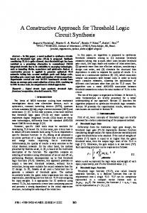
D. REPRESENTATION OF LOGICFUNCTIONS BY BINARY DECISION DIAGRAM It is an important subject in designing VLSI circuits to investigate how to represent the logical functions and process them efficiently on a computer. Usually the Boolean equation and the truth table have been used to represent digital functions; the BDD is another approach. The logical function can be accomplished by the BDD with small memory size and small calculation steps compared with the usual method. The binary decision diagram is a way to represent the logical functions by using a directed graph as shown in Fig. 1. The basic element of the BDD is a node having one input terminal (root) and two output terminals (branch0 and branchl). Each node has internal states "0" or "1" and points to one of the branches depending on the internal state, say branch0 for the "0" state and branchl for the "1" state. For example, when one traces from the top of the graph in Fig. 1, if the state of the node xi is "1" one will move to node "x2", and if "0" one will move to node "x3". Continuing this procedure, one reaches the end of the graph which is labeled by "0" and "1". This value corresponds to the solution of the logic operation. Figure 1 is an example of the representation of the logic operation f = X I .x2 + x 3 by the BDD. It is known that any logic function can be represented by the BDD.
Iroot Xl
x2 + x3
branchl
Fig. 1 The binary decision diagram (BDD). The figure shows an example ofthe logical function x i . x2 +X3.
1051-8223/99$10.00 0 1999 IEEE
3162
111. DESIGNOF RSFQ LOGICCIRCUITS BY THE BINARY DECISION DIAGRAM In order to design digital circuits based on the BDD representation, we must find the basic element which operates as the node in the BDD. This element has to switch the messenger, the particle representing the state of the system, from the root into one of the branches depending on its internal state [3]. Because the SFQ pulse can be used as the messenger, the BDD basic element can be effectively implemented by superconducting circuits. One way is to use a D2 flip-flop [6]as shown in Fig. 2. In this case, the root and the two branches in the BDD element correspond to the "Clock" and the complementary outputs, "Out" and " E t " in the D2 flip-flop, respectively. The internal state of the basic element can be changed by an input of an SFQ pulse into the complementary input, "Data" and "Data". The input of an SFQ pulse into "Data" ("Data") changes the state of the flip-flop into the "1" ("0") state,
regardless of the previous state. When an SFQ pulse is applied to the "Clock', an SFQ is outputted at "Out" ( " E t " ) if the state of the flip-flop is "1" ("0"). After the output of the SFQ pulse the state is reset to "0". Note that the BDD basic element can also be implemented by using B flop-flops [7]. Figure 3 shows an example of the implementation of the logic gates (AND, OR, XOR) by the BDD representation. These BDD gates have the following advantages over the conventional RSFQ logic gates. (i) Any combinational logic function can be performed by a series of identical basic elements, such as the D2 flipflop. (ii) The gates are dual rail, and they are data-driven selftimed [ 8 ] , [9]. Distribution of clock signals to the gate is not necessary in t h s case. (iii) The internal state is determined by the propagation of the messenger. The only requirement for the timing is that the messenger had to arrive to each gate after the transition caused by input data. (iv) Since complex logic circuits can be implemented by regular arrays of BDD basic elements, the modularity of the circuits is very large, which simplifies layout design. It should be noted here that if the complementary inputs to the first stage of the D2 flip-flop are directly ("xo", 50'') applied to the root of the next stage, the flip-flop at the first stage is eliminated as shown in Fig. 4.
Data
L5 512>