A Pipelined Configurable Gate Array for Embedded ... - CiteSeerX
Recommend Documents
SattLine. Chartwell Bratt Ltd. ISBN 0-86238-259-5. KHALIL, H. K. (1992): Nonlinear Systems. MacMillan, New York. KNUTH, D. E. (1969): The Art Of Computer ...
Jun 5, 2013 - [13] John Allen.âPhotoplethysmography and its application in clinicalphysiological measurementâ,Physiol. Meas. 28 (2007) R1âR39.
Frank Vahid*and Walid Najjar ...... [10] J. L. Hennessy and D .A. Patterson, âComputer architecture ... [15] J. Kin, M. Gupta and W. Mangione-Smith, âThe Filter.
ACM Transactions on Embedded Computing Systems, Vol. .... Alchemy. A. U1000. 16K. 4. 32. 16K. 4. 32. Motorola. MPC7455. 32K. 8. 32. 32K .... address' index field is decoded to simultaneously read out the appropriate tag ..... Table II. Dynamic Access
embedded system security focuses on the protection of application loading and ... Cost-sensitive embedded systems are used to execute end-user applications in a wide .... A description and analysis of experimental results regarding steady-.
as a free variable. The resulting low-power ... 198. Io'h Intemarional Conference on VLSI Design -January 1997 ... design to realize a processor array configurable for N ,. T, and /3. ..... ing!,â Technical Report, SERC Dept., Indian. Institute of
Abstract â We present a new architecture for signed multiplication which maintains the pure form of an ar- ray multiplier, exhibiting a much lower overhead than ...
Embedded DRAM for a Reconfigurable Array ... offs involved in the design of embedded DRAM for FPGAs. ..... ity of the DRAM is hidden from the programmer.
A New Pipelined Array Architecture for Signed Multiplication. Eduardo Costa,. Sergio Bampi. JosÑ Monteiro. UCPel, Pelotas, Brazil. UFRGS, P. Alegre, Brazil.
Rapid application development, Function Block, FPGA,. Embedded System. 1. Introduction. Early detection of system breakdown commonly necessitates a large ...
[email protected]. 3Electronics ... support for additional expansions through the use of add-on .... complex components that are needed to support com-.
Key words: Baugh-Wooley algorithm, Digital Signal Processing (DSP), Field Programmable Gate ... Applications Such as DSP, image processing and.
In this paper we present an efficient embedding of pyramids onto this architecture. The embedding has the property that neighboring nodes in the pyramid are ...
A Power-Configurable Bus for Embedded Systems. Chuanjun Zhang. Dept. of Electrical Engineering. University of California, Riverside [email protected].
here provides an architecture that supports a larger number of different SAD-based motion .... In the case of the ARM processor, it is estimated that the processor ...
[6] I. Kuon and J. Rose. Measuring the gap between. FPGAs and ASICs. Computer-Aided Design of. Integrated Circuits and Systems, IEEE Transactions.
slow, and the bit-parallel style is faster than necessary. Digit-serial algorithms have been proposed using on-line arithmetic. (most significant digit first) based on ...
Feb 19, 2011 - customised QP solver for optimal control of linear processes with constraints, which ..... Wk := LkS. â1 ..... program memory and have a counter iterating through ..... www.xilinx.com/support/documentation/data sheets/ds150.pdf.
Feb 19, 2011 - structure and accelerating the computational bottleneck in a primal-dual interior-point method. We then .... will only consider online numerical optimisation, thereby ..... movements of small blocks of data from main memory to.
Feb 24, 2016 - Field Programmable Gate Array Based Variable Speed Drive for a. Three-Phase .... This top level entity defines interconnections between.
Our new approach to embedded system security focuses on the protection ...
Cost-sensitive embedded systems are used to executing end-user applications in
a ...
Flight Critical Systems, Line Replaceable Unit , Integrated Modular Avionics, Time ... The avionics systems and software architecture of federated era was no ...
describe the stream model and its application to the BF561 to utilize low-latency ...... [33] Analog Devices, Inc. Software Development Kit (SDK) Down- loads ...
or run-time adaptation of application behavior to facilitate better performance combined ... development of middleware for self-configurable systems in the automotive sector. ...... cellphones such as the iPhone â that are less restricted than othe
A Pipelined Configurable Gate Array for Embedded ... - CiteSeerX
of OneChip processor [9] tightly couples a RISC processor ... plicitly structured to build configurable pipelines, even deep ones, but unlike ..... For classical.
A Pipelined Configurable Gate Array for Embedded Processors Andrea Lodi
very high non-recurrent engineering costs due to design and mask production. A more flexible approach introduces a reconfigurable interconnect network to connect a variety of computing elements [2], but the main drawback is that such an approach does not lead to an architectural model that makes software development easy for programmers proficient in high-level languages. A different solution exploits the improving FPGA technology, by coupling standard programmable processors, such as microcontrollers or DSP, with embedded configurable gate arrays that support application specific logic. Flexibility is enhanced thanks to the possibility to modify at deployment time the dedicated logic, making this solution more appealing because of rising mask costs and time-to-market constraints. Furthermore dynamic reconfigurability of new generation FPGAs allows one to even exploit temporal re-use through run-time modification of the instruction set, based on the currently executed algorithm (e.g. audio vs. video decoding). The main drawback of the existing solutions is that they hardly justify the cost in area due to configurable logic either because of inefficiency in the configurable unit and in the system architecture, or because of the increasing burden of the programmer, making the development of complex code very difficult. In this paper we present a new architecture tightly coupling a processor with a configurable unit. The integration of a configurable datapath in the processor core reduces any communication overhead towards functional units, thus increasing its use in more computation kernels. The approach adopted overcomes the limitations of similar preceding architectures relying on a new field configurable Gate Array, designed to extend microprocessor datapaths, and on an integrated software environment providing user-friendly tools for application development. A VLIW reconfigurable processor has been implemented on silicon to prove the effectiveness of the architecture proposed, focusing on speed-up and energy performance. Section 2 overviews previous work related to processor and FPGA coupling. In Section 3 we describe the approach adopted to design an architectural environment for the implementation of reconfigurable processors. In Section 4 a new configurable Gate Array is presented suitable for the architectural approach adopted. Section 5 describes the implementation of a prototype based on a VLIW processor, and Section 6 the related results. At last, Section 7 concludes our work with final remarks.
In recent years the challenge of high performance, low power retargettable embedded system has been faced with different technological and architectural solutions. In this paper we present a new configurable unit explicitly designed to implement additional reconfigurable pipelined datapaths, suitable for the design of reconfigurable processors. A VLIW reconfigurable processor has been implemented on silicon in a standard 0.18 µm CMOS technology to prove the effectiveness of the proposed unit. Testing on a signal processing algorithms benchmark showed speedups from 4.3x to 13.5x and energy consumption reduction up to 92%.
Categories and Subject Descriptors B.7.1 [Integrated Circuits]: Types and Design Styles— Gate arrays; C.5.3 [Computer System Implementation]: Microcomputers—Microprocessors
General Terms Design, Performance
Keywords FPGA, Reconfigurable processor, Pipeline, Energy
1.
INTRODUCTION
Energy consumption, computing power, increasing mask and design costs are the major issues in the project of today’s embedded systems. A possible solution is represented by mask configurable microprocessors, which define the processor architecture at the mask level [1]. This approach provides a user-friendly environment for application development, allowing to use a model where the required extensions are accessible as special functional units from the assembler code, however it is not efficient when specifications of the application change, with
Permission to make digital or hard copies of all or part of this work for personal or classroom use is granted without fee provided that copies are not made or distributed for profit or commercial advantage and that copies bear this notice and the full citation on the first page. To copy otherwise, to republish, to post on servers or to redistribute to lists, requires prior specific permission and/or a fee. FPGA’03, February 23–25, 2003, Monterey, California, USA. Copyright 2003 ACM 1-58113-651-X/03/0002 ...$5.00.
21
2.
RELATED WORK
which could even not be known at compile time. In fact the number of cycles needed to complete the execution may depend on the pGA pipeline status and on the values of the inputs when for example f or or while loops are entirely implemented inside the array. The computational model proposed takes advantage of the synergy between different application specific functional units tightly integrated in the same core. An FPGA behaving like a coprocessor needs to implement an entire computational kernel to achieve high throughput because the communication overhead to the processor core is considerable. As a consequence when a kernel is composed of both functions suitable to be mapped in an FPGA and operators which could not be efficiently implemented in the configurable unit, it is often completely executed in the processor core, leaving the array unused. In our model the communication overhead between the pGA and the other functional units is as small as possible, thus allowing to distribute the different operations included in a single kernel to the functional unit that best fit them. Wide multipliers, variable shifters, MACs, which are so difficult to implement efficiently in FPGA, could be executed in dedicated hardwired functional units, while the configurable unit exploits parallelism of even small portion of kernels. In this way utilization of the pGA considerably increases, justifying its cost in terms of area for a wide range of applications.
Probably the first prototype to couple a configurable hardware with a general purpose processor was the PRISM machine [3] which consisted of a multi-FPGA board plugged into a host system. The main contribution was to introduce a new computational model where the configurable hardware was accessed through instruction set extension. A similar approach was adopted by the Spyder architecture [4], but both machines suffered from size limitations of FPGAs at that time, and from inter-chip communication overhead between processor and configurable hardware. One step further was taken when several prototypes integrated FPGA on the same chip as the microprocessor, to achieve a higher communication bandwidth. Two main categories can be identified depending on the degree of FPGAprocessor coupling: tightly coupled and loosely coupled. In the first case the reconfigurable array is seen just as another functional unit in the processor datapath, thus fed with data by the register file. Such prototypes include PRISC [5], Chimaera [6, 7] and ConCISe [8]. The main limitation of these architectures is that the reconfigurable hardware supports only combinatorial circuits, in order to fit in the processor pipeline stages. Although this approach has the advantage of keeping the processor control logic unchanged, unfortunately configurable hardware is not able to exploit parallelism, resulting in poor speedups. The first version of OneChip processor [9] tightly couples a RISC processor with a multi-cycle FPGA, but this resulted in a memory bandwidth bottleneck. Therefore, in order to overcome this limitation, a direct access to memory of the gate array was provided [10] with dedicated instructions accessing blocks of memory, but again complex addressing strategies can hardly be handled with this kind of solutions. In loosely coupled architectures the reconfigurable array is integrated as a co-processor operating asynchronously, with a direct access to memory and connected to the processor host via a bus. This category includes the GARP processor [11, 12]. Since the FPGA is external, there is an overhead due to explicit communication using dedicated instructions to move data to and from the array, thus the use of the array is convenient only for kernels executed for a great number of clock cycles without the intervention of the processor.
3. 3.1
3.2
Architectural Implementations
From an implementation point of view, the introduction of the pGA requires minor changes of the system architecture. System control, memory and I/O interface are still operated by the processor core, while modifications needed are bound to the peculiarities of the configurable unit: high in/out band-width and variable latency. The pGA can receive up to four 32-bit words and produce up to two 32-bit words as result, thus the register file needs to provide at least 4 ports for read and 2 for write operations. We can distinguish modifications needed on the base of the underlying processor architecture:
3.2.1
Superscalar
In superscalar processors a number of units are able to execute instruction concurrently to exploit instruction level parallelism. In such systems dynamic scheduling is performed relying on complex hardware structures which analyze interdependencies between instructions executed in different functional units. The register file is already provided with multiple read/write ports which could be used to feed the pGA too. At the same time dynamic scheduling already provides a solution for the variable latency problem, so that no real modifications are needed.
SYSTEM ARCHITECTURE Overview
The approach adopted in the architecture proposed is to provide a microprocessor with an additional pipelined runtime configurable datapath (PiCo Gate Array, pGA), capable of introducing a large number of virtual application specific units. The reconfigurable unit is tightly integrated in the processor core, just like any other functional unit, thus receiving inputs from the register file and writing results back to the register file. Differently from [5] the pGA does not only allow multicycle latency functions, but it is explicitly structured to build configurable pipelines, even deep ones, but unlike PipeRench [13] which performs reconfiguration of a pipe stage in a clock cycle as the data fill in the device, the pGA has a traditional approach, assuming that a configuration is stored to be used for a sufficiently long time, in order to keep configuration power consumption low. Each configuration implements a peculiar data-path with a number of stages suitable for the function to be executed
3.2.2
VLIW
In Very Long Instruction Word (VLIW) processors independent operations are grouped into very long instructions, supporting the parallel execution of a number of functional units. Dependencies checking, in order to find independent operations, and following scheduling is done at compile time. While multi-ported register file is already provided because of the necessity to feed a number of functional units, the pGA must be supported with special hardware to take into count its variable latency. Read-After-Write (RAW) is the only data dependency to take care of as it is the only one
22
.
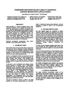
4x32−bit input data bus from Reg File 2x32−bit output data bus to Reg File 192−bit configuration bus from Configuration cache
2
loop−back
VERTICAL CONNECTION BLOCK
12 global lines to/from RF
2
RLC
INPUT LOGIC
2 2
LUT 16x2 2
12
LUT 16x2 2
OUTPUT EN LOGIC, REGISTERS
configuration bus
pGA CONTROL UNIT
HORIZONTAL CONNECTION BLOCK
SWITCH BLOCK
2 2
CARRY CHAIN
2
pGA control unit signals
Figure 1: PiCoGA structure that cannot be granted by the compiler which doesn’t know the pGA latency at compile time. Introducing a register locking mechanism is the least intrusive way to handle the problem: when a pGA instruction is decoded, its destination registers are locked so that if a following instruction needs to access them, the processor execution is stalled. When the pGA completes the write-back operation, registers are unlocked and normal processor execution is restored. Anyway, in order to avoid frequent stalls of the processor pipelines, the compiler needs to schedule even pGA instruction, based for example on their average latency.
3.2.3
a sequence of pGA instructions can be processed filling the pipeline in order to exploit parallelism. Moreover the configurable unit should preserve its state across instruction executions. A new pGA instruction may directly use the results of previous ones, thus reducing the pressure on the register file. Since most of the control logic would be executed in the standard processor pipeline, the configurable unit should have a granularity suitable for multi-bit data-path implementations, but at the same time it should be flexible enough to compensate the other functional units for the kind of computations they are not efficient. Finally a tight integration in the processor core gives the opportunity to use the pGA in many different computational cores, therefore run-time reconfiguration is necessary to support new sets of dynamically defined instruction.
RISC
When intagrating the pGA into a RISC core, further to implementing a register locking mechanism, considerable modifications affect the register file which needs to be redesigned multiport. Nevertheless the increment in area implied can be considered negligible when compared to memories and the configurable unit. As in VLIW processors special care must be taken by the compiler when scheduling pGA instruction with variable latency.
4.
4.1
PiCoGA Structure
The pGA is an array of rows, each representing a possible stage of a customized pipeline. The width of the datapath obtained should fit the processor one, so each row is able to process 32-bit operands. As shown in Figure 1, each row is connected to the other ones with configurable interconnect channels and to the processor register file with 6 32-bit busses. In a single cycle four words can be received from the register file and up to two can be produced for writeback operation. The busses span the whole array, so that any row can access them, improving routability. Pipeline activity is controlled by a dedicated configurable control unit, which generates two signals for each row of the array. The first one enables the execution of the pipeline stage, allowing the registers in the row to sample new data. In every cycle only rows involved in the piece of computation to be executed in that cycle are activated, in a dataflow fashion. In this way a state stored in flip-flops inside the array can be correctly held and at the same time unnecessary power dissipation is avoided. The second signal controls ini-
PIPELINED CONFIGURABLE GATE ARRAY
In the past a few attempts have been carried out in order to design a configurable unit tightly integrated in a processor core and their study led to some guidelines that have to be followed to achieve a significant gain in the performance of the overall system. First of all the configurable unit should be able to perform complex functions that require multi-cycle latency. The pGA is designed to implement a peculiar pipeline where each stage corresponds to a piece of computation, so that high throughput circuits can be mapped. The array is also provided with a control unit which controls pipeline activity, just as if it was a complete additional datapath. In this way
23
2
2
2
2
constant INITIALIZATION LOGIC 2
INPUTS INVERT/SWAP LOGIC 4
4
loop−back
LUT 16x2
EN
pGA control unit signals
LUT 16x2
CARRY, OR, XOR, >, >=
OUTPUT
REGISTERS
2
2
LOOKAHEAD CHAIN
Figure 2: Reconfigurable Logic Cells logic structure tialization steps (see 4.2) of a state held inside the array. In order to support the implementation of high level language control constructs such as while and for loops, each row can generate a signal for the control unit. These signals could for example represent the boolean value resulting from a comparison performed in the array core. Hence pipeline activity can depend on data values as needed in while loops. Since most of the remaining portion of control logic not executed in the processor standard dataflow is implemented in the configurable control unit, the array core can be datapath oriented. Therefore the pGA has a 2-bit granularity for both interconnections and LUTs, which is a good compromise taking into count that bit-level operators such as bit permutation, which are frequent in cryptography algorithms, are badly supported by other functional units. Each row is composed of 16 Reconfigurable Logic Cells (RLC) and a configurable horizontal interconnect channel. Vertical channels are wider (12 pairs) than horizontal ones (8 pairs) because computation mainly flows in the vertical direction as a consequence of the array organization. Switch blocks adjacent to each RLC connect vertical and horizontal wires.
pGA_init(); while (cond) { out=pGA_op(b); ... } pGA_init(d); while (cond) { out=pGA_op(b); ... }
RLC LUT a LUT
RLC
t d
b RLC LUT a LUT
RLC
t
Figure 3: State initialization conditions with relative c source and modified code
A Reconfigurable Logic Cell (RLC) is composed of a cluster of 2 LUTs. LUTs have 2-bit granularity, that is 4-bit inputs and 2-bit outputs (4:2). A total of 6 inputs from the configurable interconnect channels are provided to the RLC which can be used to implement logic functions with different granularity combining the two LUTs together. A two level multiplexing stage controlled by two of the inputs performs the combination of LUT outputs. In this way mapping of either a 6:1 or a 5:2 or 4:4 logic function is allowed. An RLC contains 4 registers, one for each output, which are controlled by the configurable control unit. RLC outputs are internally routed back to the input block, in order to implement the cascade of two LUTs or logic holding a state such as accumulators. On the feed back path a block controlled by the control unit is introduced
to support different kinds of state initialization. Given the array structure, four possible cases have to be considered, depending on two factors: • initialization of the state with a constant or with a variable which necessarily comes from another RLC; • use of the internal feed back path or implementation of an external loop through other RLCs. In Figure 3, the four cases are represented with a portion of c-like language source code together with the modified
Figure 4: PiCoGA configurations loaded in cache layers and blocks code where the while construct is executed in the processor standard datapath whereas the computation inside the loop is mapped in the pGA. The implementation with RLC resources is also shown. Each RLC contains a dedicated carry chain block performing a level 1 look-ahead logic. Dedicated wires along each row, directly connecting configurable cells, are also provided to have fast propagation of carry signals. Even though a standard-cells synthesis and automatic back-end flow was adopted for the design of RLC logic, comprising carry logic, a 32-bits addition at 150M Hz in a 0.18µm process was achieved. A single RLC can implement a 2-bit adder using the two LUTs to compute both the results with carry-in equal to 0 or to 1. The same multiplexers, which combine LUT outputs, can be used to propagate the right result on the base of the carry-in value in a carry-select fashion. Besides sum carry logic, other bit-serial computations have been introduced which could take advantage of the fast dedicated wires, such as comparison, or and xor operators. Exploiting the input block of the RLC to invert signals, even more operators can be efficiently mapped in the same way.
4.3
Three different approaches have been adopted to overcome these limitations. First of all the pGA is provided with a first level cache, storing 4 configurations for each logic cell [14, 15]. Context switch takes place in one clock cycle, providing 4 immediately available pGA instructions. Further increase in the number of functions simultaneously supported by the array can be obtained exploiting region partitioning. The array is structured in blocks composed of 8 rows each. A block represents the minimum unit of the pGA that can execute an instruction and be configured independently. Two or more blocks can be combined together to implement larger functions. If we consider an array with 24 rows, 3 different instructions occupying just one block could be supported for each layer of the cache, resulting in a total of up to 12. The pGA may execute concurrently one computation instruction and one reconfiguration which can store the next instruction to be performed. In this way cache miss should be highly reduced, even when the number of configurations used is large. Finally reconfiguration time can be shortened exploiting a wide configuration bus to the pGA. The RLCs in a row are written in parallel with 192 dedicated wires, taking up to 16 cycles to have a complete reconfiguration. A dedicated second level cache on-chip is needed to provide such a wide bus, while the whole set of available functions can be stored in an off-chip memory.
Configuration Caching
Since the pGA is tightly integrated in the processor core, it could be used frequently, for many different computational kernels. However reconfiguration of gate arrays can take hundreds but most frequently thousands of cycles, depending on the re-programmed region size. Although execution can still continue on other processor resources, scheduling will hardly find enough instructions to avoid stalls that could overcome any benefit from the use of dynamically configurable arrays. Furthermore in some algorithms the function to be implemented is only known at the time it has to be executed, so that no preventive reconfiguration can be done. In such cases many computational kernels cannot take advantage of the presence of a configurable unit, leaving it unused during their execution in the processor standard datapath. The efficiency of the overall system in terms of performance density can be greatly affected, hardly justifying the area overhead introduced by the pGA.
5.
PROTOTYPE IMPLEMENTATION
In order to prove the effectiveness of the architectural approach proposed, a specific implementation of a reconfigurable processor has been designed in a 0.18 µm 1.8V, 6 Metal Layers CMOS technology. The basic architecture chosen is a VLIW processor which can already rely on a multiport register file to feed the wide in/out busses of the pGA. The register locking mechanism was implemented together with the design of an interface block handling configuration caching and writeback operation. Although a superscalar processor seems to be the best choice because of its degree of parallelism and dynamic scheduling, the hardware complexity involved could not be worthwhile with respect to a VLIW
25
XIRISC DATA PATH WRITEBACK CHANNELS
DATA
INSTRUCTION REGISTER FILE
DECODE LOGIC
MEMORY
CHANNEL 1
MUX DATA CHANNEL 2 DATA MEMORY
PiCoGA/Processor Interface CONFIGURATION
PiCoGA DATA PATH
CACHE
PiCoGA CONTROL UNIT
PiCoGA WRITEBACK CHANNEL
CONFIG. CONTROL
PiCoGA
Figure 5: Implemented prototype architecture implementation. In fact most of the algorithms analyzed in the PiCoGA have fixed latency, so that scheduling at compile time is extremely efficient, while parallel execution of microprocessor and configurable datapath is provided. A software development environment based on a customization of the GNU-Gcc toolchain as shown in [16] has been used to support architecture programming and benchmarking. The availability of a software profiling environment offers an appropriate mean to manually determine critical computation kernels that could be implemented on the pGA. Starting from the portions of C code identified, configurations for the array have been generated through manual mapping, in order to find the number of rows needed, latency and throughput. Since each row of the PiCoGA occupies 0.6mm2 a maximum of 32 rows was considered which would be more than 50% of the total area of the reconfigurable processor, including instruction, data and configuration cache memories. For energy consumption performance, measures were conducted on a test-chip of the configurable processor with 8 PiCoGA rows, implementing several algorithms including DES encryption. Energy consumption of other algorithms has been estimated through cycle-base analysis, exploiting the measured average consumption of memories, VLIW core and PiCoGA rows.
5.1
be easily customized. It is based on a classic five-stages pipeline [18]. Two 32-bit instructions are fetched each clock cycle from the Instruction cache, decoded and executed concurrently determining two different execution flows (data channels). A set of multiple latency, hardwired functional unit is provided, performing general purpose DSP calculations such as 32-bit and 64-bit multiplication, multiplyaccumulation, parallel byte-wise arithmetics and branch decrement operations. The architecture is fully bypassed, to maintain high data throughput through hardware resources. The addition of the pGA extends the architecture to three concurrent execution flows, allowing to maintain a very high access rate to memory exploiting the two hardwired channels, while application specific computational cores are more efficiently implemented on the configurable unit. A 32-slots register file features 4 source registers feeding the two hardwired data channels, which can also be used for the pGA. On the other hand the number of destination registers have been extended from 2 to 4 in order to support completely independent write-back operations. This avoids the introduction of dedicated logic handling competition for the write ports of the register file as far as pGA instructions have variable latency. In order to support the integration of the pGA in a processor core, the instruction set has to be extended just as when new functional units are added. In the case of a configurable unit usually both configuration and execution instructions are provided, to support preventive load from the secondlevel cache of the functions to be executed.
XiRisc Processor
XiRisc (eXtended Instruction set Risc) [17] is an open core VLIW processor, providing a flexible architecture which can
26
Algorithm DES encryption CRC Median filter (parallel) (24bit word, 8 samples) Median filter (sequential) (8bit word, 256 samples) Motion estimation Motion prediction
Rows occupation 5 11 32
1st level cache layers 1 1 1
17
4
24 12
1 4
Table 1: PiCoGA area required for some signal processing algorithms
Algorithm DES encryption CRC Median filter (parallel) (24bit word, 8 samples) Median filter (sequential) (8bit word, 256 samples) Motion estimation Motion prediction
Speed-up (vs. Std. VLIW) 13.5x 4.3x 7.7x
pGA in/out channels Data dependency Area
6.2x
Memory accesses
12.4x 4.5x
Area Memory accesses, area
Bottleneck
Table 2: Speedups and bottlenecks for some signal processing algorithms
5.2
Interface Logic
which ranges from 5 rows required for the round f implementation of the DES encryption algorithm to 32 rows for a parallel implementation of a median filter. Since our architectural model involves strong interaction between reconfigurable array and standard VLIW resources (e.g. typical ALU operations), in order to achieve better results, computation is often split into few pGA functions, each mapped on a different layer of the first level cache. For example, a sequential implementation of the median filter can be split into 4 pGA instruction, thus involving each available cache layer. In this case, table 1 reports the maximum number of rows required by these 4 functions. Table 2 shows speedups achieved referring to the implemented reconfigurable VLIW architecture. pGA has proven to be very flexible, allowing performance gain for every tested algorithm, ranging from 4.3x to 13.5x. Speedup was calculated counting the number of execution cycles with respect to those of the reference XiRisc VLIW standard architecture, namely a 5 stage pipeline processor with two concurrent parallel datapaths, two instruction fetched each cycle and dedicated functional units such as a multiplieraccumulator and a hardware branch-decrement unit. Table 2 also shows the computation bottleneck for each tested algorithm. Thanks to VLIW approach, which allows concurrent memory and pGA operations, memory access bandwidth is increased, and also memory-intensive algorithms (such as motion prediction) become efficient. Nevertheless, few algorithms (e.g. median filter, motion estimation and prediction) could achieve higher speedups with an increased bandwidth between pGA and memory, for example providing a direct connection. This issue could be overcome with a different architecture providing a wide data bus connecting memory and reconfigurable device and allowing complex addressing. pGA is designed to be easily included in this kind
Integration of the pGA in the XiRisc core needs some interface logic. First of all register locking mechanism must be introduced, together with a FIFO buffer of destination registers of the instructions currently executing in the pGA. Interface logic writes destination registers as soon as the results from the pGA are ready, exploiting dedicated channels. In this way writeback operations of the configurable unit is completely handled by dedicated logic different from the control logic of the core, thus left unchanged. Moreover a configuration control block has been designed to handle configuration caching. Dedicated logic decodes the pGA instructions determining the function to be executed or loaded. A status table, similar to the one used in [10], keeps the memory address of the available pGA functions and a track of the block and the layer in the first-level cache of the stored configurations. Finally undesired processor stalls could happen if a configuration load instruction is issued when a reconfiguration process is already ongoing. From the processor point of view the pGA would be a busy functional unit and no further instructions could be executed. This condition can frequently occur when scheduling a preventive load of several configurations to be used later. Better performance could be achieved allowing the parallel execution of any following instruction different from a configuration load one. Thus the solution adopted is to provide the interface logic with a buffer of issued configuration load instructions that are performed one after the other with no intervention of the processor core.
6. RESULTS PiCoGA was tested on several signal processing algorithms, in order to explore speed-up and power consumption achieved. Table 1 shows the pGA area needed to map the algorithms,
27
CRC (1Kbyte data) Only VLIW
Median Filter (40 samples, 24 bit word size, window size 8)
VLIW + PiCoGA
Only VLIW VLIW Core 23%
Data Mem. 38%
PiCoGA 24%
Data Mem. 29%
VLIW Core 14%
Instr. Mem. 39%
VLIW Core 21%
7.24 uJ (4381 cycles)
2.47 uJ (1444 cycles)
Data Mem. 38%
Instr. Mem. 34%
1.06 uJ (570 cycles)
Figure 8: Energy consumption for Median Filter (parallel implementation)
DES (64 bit)
Instr. Mem. 37%
VLIW Core Data Mem. 20% 41%
Instr. Mem. 38%
6.42 uJ (3352 cycles)
Figure 6: Energy consumption for CRC algorithm
VLIW Core 24%
PiCoGA 8%
Instr. Mem. 33%
23.14 uJ (14385 cycles)
Only VLIW
VLIW + PiCoGA
VLIW + PiCoGA ory roughly scales with speed-up. In fact, the execution on pGA allows an improved efficiency for data management (e.g. data stored locally on pGA), thus reducing data memory consumption. Fig. 6, 7 and 8 also show that considering the overall energy consumption of the proposed architecture, pGA contribution ranges from 4% to 24%, that is from 0.3% to 6.7% of the original consumption. Fig. 9 shows the relation between speed-up and energy consumption reduction. For the reasons mentioned above, this relation is linear, with a small overhead due to pGA contribution. Results show that energy consumption is reduced for algorithms presenting a speedup higher than 1.5x. Array reconfiguration requires additional energy consumption due to context switches among the 4 cached configurations inside the array but mostly to second level configuration cache accesses. This contribution is not present during normal execution, therefore the average additional energy consumption due to reconfiguration depends on the number of execution cycles. Fig. 10 shows the relation between the overall energy consumption (including the reconfiguration overhead from second level cache), and the number of execution clock cycles. The impact of this energy consumption overhead becomes negligible when a given configuration is used for more than 1000 cycles. Typically, a configuration is active for a far larger number of cycles. For instance, 1000 cycles are needed to encrypt 80 bytes with DES algorithm or to compute the parity check of 300 bytes. Therefore, in most situations, it’s possible to neglect reconfiguration overhead, considering only execution energy. Results are shown in fig. 11, where improvement due to pGA is evident.
PiCoGA 4% VLIW Core Data Mem. 22% 39%
Data Mem. 38%
Instr. Mem. 36%
0.187 uJ (106 cycles)
Figure 7: Energy consumption for DES algorithm of architectures. Available array area is a bottleneck for a few algorithms (e.g. parallel implementation of median filter, motion estimation and prediction), where there is a huge level of parallelism which could be exploited. For other algorithms (e.g. CRC) exploitable parallelism is low, thus performances show an upper bound which is independent from hardware specifications. Finally, also the number of input/output channels from/to pGA could represent a bottleneck when functionality to be mapped requires more than 4 inputs or more than 2 outputs, but typically in these cases the real bottleneck is memory bandwidth. Only in rare cases when all needed data are already present in the register file (e.g. DES keys), the number of in/out channels is a real limitation. Power consumption is the other key issue. For classical processor-based architectures, the main source of power consumption is due to memory accesses. Measurements on a standard VLIW architecture show that the percentage of energy required by instruction and data memory are typically above 75% of the overall value, and that every tested algorithm roughly presents the same distribution (Fig. 6, 7 and 8). Since every clock cycle a new instruction is fetched, the only way to reduce instruction memory energy consumption is to reduce the number of execution cycles. In fact, instruction memory consumption scales proportionally with speedup, therefore a VLIW architecture enhanced by the pGA achieves both speedup (table 2) and instruction memory consumption reduction. Several tests have shown that also accesses to data mem-
7.
CONCLUSIONS
A new configurable unit, suitable for reconfigurable processor implementations, has been presented. Featuring a run-time reconfigurable pipelined datapath, the PiCoGA can be tightly integrated in many different processor architectures, acting as an additional functional unit addressed through instruction set extension. A prototype including the pGA and a standard VLIW processor has been implemented, and testing showed that this approach is very flexible, allowing a more efficient implementation of a wide range of signal processing algorithms. Through application specific instructions mapped on pGA, speedups ranging from 4.3x to 13.5x
28
DES
13
1
Energy reduction
1/(Normalized energy reduction)
14
12 11 10 9 8 7
0.8
Median Filter
0.7
CRC
0.6
DES
0.5
Median Filter
6
0.9
0.4
5
Motion Pred. 0.3
4
CRC
3
0.2
2
0.1
1 1
2
3
4
5
6
7
8
9
10
11
12
13
14
10
10
3
10
4
10
5
Execution cycles
Speed−up
Figure 9: Speedup vs. energy consumption for several signal processing algorithm
2
Figure 10: Energy consumption vs. number of clock cycles between two reconfigurations
Normalized Energy Histogram 1 0.9 0.8
Only VLIW
0.7 0.6 0.5
VLIW + PiCoGA
0.4 0.27
0.3
0.1
0.22 0.15
0.2 0.076
0
DES
CRC
Median Motion Filter Prediction
Figure 11: Normalized energy consumption for some signal processing algorithms
10.
are achieved, while instruction and data memory accesses are reduced allowing an energy consumption reduction up to 93%.
8.
[1] Tensilica Inc. http://www.tensilica.com. 2001. [2] H. Zhang, V. Prabhu, V. George, M. Wan, M. Benes, A. Abnous, J.M. Rabaey. “A 1V Heterogeneus Reconfigurable Processor IC for Baseband Wireless Applications” In Proceedings of the 2000 IEEE International Solid State Circuits Conference. [3] P. Athanas and H. Silverman. Processor reconfiguration through instruction-set metamorphosis. IEEE Computer, 26(3):11–18, March 1995. [4] C. Iseli and E. Sanchez. Spyder: a SURE (SUperscalar and REconfigurable) processor. Journal of Supercomputing, 9(3):231–252, 1995. [5] R. Razdan and M. Smith. A high-performance microarchitecture with hardware-programmable
ACKNOWLEDGEMENTS
The authors would like to thank L. Lavagno, C. Passerone and A. La Rosa of the Politecnico di Torino for software tools development and STMicroelectronics for funding and support.
9.
REFERENCES
ADDITIONAL AUTHORS
Additional authors: Andrea Cappelli (ARCES, University of Bologna), Roberto Canegallo (NVM-DP Department of STMicroelectronics CR&D) and Roberto Guerrieri (ARCES, University of Bologna).
29
functional units. In Proceedings of the 27th Annual International Symposium on Microarchitecture, November 1994. [6] S. Hauck, T. Fry, M. Hosler, and J. Kao. The Chimaera reconfigurable functional unit. In Proceedings of the IEEE Symposium on FPGAs for Custom Computing Machines, pp.87-96, Napa Valley, California, April 1997. [7] Z.A. Ye, N. Shenoy, and P. Banerjee. A C compiler for a processor with a reconfigurable functional unit. In Proceedings of the ACM/SIGDA International Symposium on Field Programmable Gate Arrays, February 2000. [8] B. Kastrup, A. Bink, and J. Hoogerbrugge. ConCISe: A compiler-driven CPLD-based instruction set accelerator. In Proceedings of the Seventh Annual IEEE Symposium on Field-Programmable Custom Computing Machines, pp.92-100, Napa Valley, California, April 1999. [9] R. Wittig, and P. Chow. OneChip: An FPGA Processor With Reconfigurable Logic. In Proceedings of the IEEE Symposium on Field-Programmable Custom Computing Machines, pp.126-135, Napa Valley, California, March 1996. [10] J. Jacob, and P. Chow. Memory Interfacing and Instruction Specification for Reconfigurable Processors. In Proceedings of the ACM/SIGDA International Symposium on Field Programmable Gate Arrays, pp.145-154, Monterey, California, February 1999. [11] T. Callahan, J. Hauser, and J. Wawrzynek. The Garp architecture and C compiler. IEEE Computer, 33(4):62–69, April 2000.
[12] T. Callahan and J. Wawrzynek. Adapting software pipelining for reconfigurable computing. In Proceedings of the International Conference on Compilers, Architecture, and Synthesis for Embedded Systems (CASES), 2000. [13] S. C. Goldstein, H. Schmit, M. Budiu, S. Cadambi, M Moe and R. Taylor. PipeRench: A reconfigurable architecture and compiler. In Computer, 33(4): 70-77, April 2000. [14] A. DeHon. DPGA-Coupled Microprocessors:Commodity ICs for the Early 21st Century. In Proceedings of the IEEE Symposium on Field-Programmable Custom Computing Machines,pp.31-39, Napa Valley, California, April 1994. [15] S. Trimberger, D. Carberry, A. Jhonson and J. Wong. A Time Multiplexed FPGA. In Proceedings of the IEEE Symposium on Field-Programmable Custom Computing Machines ,pp.34-40, Napa Valley, California, April 1997. [16] A. La Rosa, L. Lavagno, C. Passerone “A software development tool chain for a reconfigurable processor” In Proceeding of the 2002 Int. Conf. on Compilers, Architecture and Synthesis for Embedded Systems. [17] F. Campi, R. Canegallo and R. Guerrieri. Ip-reusable 32-bit vliw risc core. In in Proceedings of the 27th European Solid State Circuits Conference, pages 456–459, 2001. [18] D. Patterson and J. Hennessy. Computer Architecture: A Quantitative Approach. Morgan Kaufmann, 1991.