JOURNAL OF SEMICONDUCTOR TECHNOLOGY AND SCIENCE, VOL.7, NO.2, JUNE, 2007
67
A Sense Amplifier Scheme with Offset Cancellation for Giga-bit DRAM Hee-Bok Kang*, Suk-Kyoung Hong*, Heon-Yong Chang*, Hae-Chan Park*, Nam-Kyun Park*, Man Young Sung**, Jin-Hong Ahn*, and Sung-Joo Hong*
Abstract—To improve low sense margin at low voltage, we propose a negatively driven sensing (NDS) scheme and to solve the problem of WL-to-BL short leakage fail, a variable bitline reference scheme with freelevel precharged bitline (FLPB) scheme is adopted. The influence of the threshold voltage offset of NMOS and PMOS transistors in a latch type sense amplifier is very important factor these days. From evaluating the sense amplifier offset voltage distribution of NMOS and PMOS, it is well known that PMOS has larger distribution in threshold voltage variation than that of NMOS. The negativelydriven sensing (NDS) scheme enhances the NMOS amplifying ability. The offset voltage distribution is overcome by NMOS activation with NDS scheme first and PMOS activation followed by time delay. The sense amplifier takes a negative voltage during the sensing and amplifying period. The negative voltage of NDS scheme is about -0.3V to -0.6V. The performance of the NDS scheme for DRAM at the gigabit level has been verified through its realization on 1-Gb DDR2 DRAM chip.
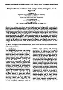
I. INTRODUCTION It will be able to continue to shrink its chip technology through at least 2009 to about 20nm-30nm range. Recent breakthroughs in the improved manufacturing methods have sparked considerable excitement about the nanoscale memories. Memory circuits, such as dynamic random access memory (DRAM) arrays, have increased in complexity and density over time. To meet the technology trend, the memory circuits should adopt the low voltage and low power based scheme [1][2]. The trend for low voltage and low power is shown in Fig. 1. The PC based DRAMs such as DDR1, DDR2, DDR3, etc. go down to near to 1.0V and the mobile application based DRAMs go down to sub 1.0V with technology scaling. In general for low voltage operation in MOS transistor based circuit, the threshold voltage (Vt) of MOS device should be reduced to low threshold voltage value. But the low Vt value in MOS device induces a large sub threshold leakage current level, producing large stand-by
Index Terms—DRAM, charge-transferred presensing (CTPS), negatively-driven sensing(NDS), free-level precharged bitline(FLPB), sense amplifier offset voltage, threshold voltage distribution.
Manuscript received Mar. 20, 2007; revised May 28, 2007. * R&D Div., Hynix Semiconductor, Ichon, 467-701, Korea E-mail:
[email protected] ** Department of Electrical Engineering, Korea Univ., Seoul, 136701, Korea E-mail:
[email protected]
Fig. 1. The trend of operation voltage in PC and mobile based DRAM.
68
HEE-BOK KANG : A SENSE AMPLIFIER SCHEME WITH OFFSET CANCELLATION FOR ~
current and active dynamic current level. If a high Vt, the power consumption from sub threshold leakage current could be reduced, but a large speed delay induces performance degradation at the sensing circuit. One potential limitation regarding the use of a high Vt device in sense amplifier is that the speed of the sense amplifier may be reduced. The sense amplifier circuit typically has activation lines used to activate the data lines responsive to the values stored in the memory cells. To reduce standby currents, one of the activation lines may be grounded prior to a memory read cycle. The signal on the grounded activation line must then pass the entire range from ground to VDD to pull the data line to the desired state. The need for this full range swing reduces the response time of the sense amp circuitry. As operating voltages decrease, the sense amp circuit becomes slower, because of the lower NMOS gate-tosource voltage. In DRAM a lot of the power consumption is likely from the charging and discharging current at bitlines (BLs) in a memory cell array. The voltage reduction at BLs directly related to power reduction by the power consuming relationship of P=CV2f. And another issue in device scaling down is very likely that one or more shorts will occur between a WL and a BL [3]. A WL-toBL short typically is a point defect that shorts together a particular row line to a perpendicular data line. The short faults increase the standby current and make difficulty in the negatively biasing word line (WL) scheme. As DRAM array sizes grow, however, row-to-column shorts become more prevalent. Redundancy rows and columns are created within the DRAM array in combination with address redirection circuitry to substitute functional spare rows and columns for those that are shorted. Even though this on-chip redundancy allows for the repair of a DRAM integrated circuit device, it is important to note that the shorted columns and rows are not disconnected from the array circuitry. The shorted columns and rows are merely no longer addressed by the array's address decode circuitry. Disconnection of the shorted rows and columns from the array circuitry is impractical with presently available technology due to the small pitch used to fabricate DRAM arrays. The repair of row to column shorts through redirected addressing does not eliminate the presence of shorts within the array, nor does it eliminate the potential for biased voltage pull
down with the attendant problems of excessive standby current, read and write operations resulting in invalid data and possible damage to cell capacitors within the array. For example, one serious problem is that of an increase in the quiescent standby current because of a defect in the circuit. To solve the problem of WL-to-BL short, a variable bitline reference scheme with free-level precharged bitline (FLPB) scheme is adopted. To overcome the sensing delay in the conventional sensing scheme, we propose a negatively driven sensing (NDS) scheme [4]. The NDS scheme achieves high performance properties of fast sensing speed and high data transfer rate at the sub-1.0V sensing voltage. NDS scheme automatically provides the dual operating voltage levels between BL voltage in cell array region and sense amplifier voltage in sense-amplifier area. The sense amplifier circuit and the bit line architecture determine the signal limit for DRAM cell readout. Increasing memory sizes, smaller feature sizes and lower operating voltages make it more important to understand the cell signal sensing operation, the signal of memory cells and the limiting factors of process and circuit design. Measurements analysis of the sense amplifier offset distribution gives further insight into the sensing limitations. The process variations in the latch NMOS and PMOS transistors have been evaluated. The threshold voltage offset occurring in the latch type sense amplifier has been analyzed. From evaluating the sense amplifier offset voltage distribution of NMOS and PMOS, we learned that PMOS has more large distribution in threshold voltage variation than that of NMOS. The offset voltage distribution is overcome by NMOS activation first and PMOS activation followed by time delay in large voltage range. But there is limit for more improving in low voltage operation range. In this paper we use the NDS scheme for improving the sense amplifier offset voltage contribution using the conventional sense amplifier circuit and NDS control scheme.
II. CHARGE-TRANSFERRED PRESENSING (CTPS) AND CONVENTIONAL SENSING SCHEME To improve the sensing performance in low voltage,
JOURNAL OF SEMICONDUCTOR TECHNOLOGY AND SCIENCE, VOL.7, NO.2, JUNE, 2007
69
Fig. 4. The conventional sense amplifier circuit details. Fig. 2. The circuit details of charge-transferred presensing (CTPS) scheme.
Fig. 5. The timing waveforms of the conventional sensing scheme. Fig. 3. The timing details of charge-transferred presensing (CTPS) scheme.
charge-transferred presensing (CTPS) scheme [1] has been proposed. The circuit and timing waveform of the conventional CTPS are shown in Fig. 2 and Fig. 3. But it requires additional transistors for transfer gates and very accurate reference level is required to have presensing effect. The SA and BL are isolated by the tranfer-gate of BISH. Here, the BISH is used for transferring the stored charge from BL to SA nodes. The BL is precharged to one-half of the power supply voltage for the array (VCORE), and the SA node is precharged at a higher level than VCORE. When the BISH level is a low level, WL is activated, and the data of memory cell is transferred to BL. Charge-transfer to BL from SA is complete when the original level of (V BISH-Vtn) is
reached on the BL and a large variation of readout voltage α appears on the SA node pair. The circuit of conventional or normal sensing scheme is shown in Fig. 4. In general the low threshold voltage (low Vt) transistors are adopted for the n and p-channel amplification. However, with even low Vt transistors the amplification margin at low VDD voltage of near 1.0V is reduced by the current degradation of n and p-channel devices. The major timing waveforms of the conventional scheme are shown in Fig. 5. The operation voltage range of the CTPS and conventional sensing scheme is the ground voltage to VDD. The performance upgrade is limited by the way of low Vt policy in the aspect of process difficulties and sub-threshold leakage current damage. With the mismatches in the threshold voltage of YI gates and an
70
HEE-BOK KANG : A SENSE AMPLIFIER SCHEME WITH OFFSET CANCELLATION FOR ~
asymmetric resistance model, the CTPS and the conventional sensing scheme suffer from BL flipping when the sensing-to-YI delay is below about a few nanoseconds.
III. NEGATIVELY DRIVEN SENSING (NDS) AND FREE-LEVEL PRECHARGED BITLINE (FLPB) SCHEME To improve low sense margin at low voltage, we propose a negatively driven sensing (NDS) scheme. The circuit of the proposed NDS scheme is shown in Fig. 6. The BL of cell array and SA_BL of sense-amplifier (S/A) are isolated by transfer-gate of BISH and BISL of PMOS transistors. The n-channel and p-channel amplifications are controlled by the control signals of SAN and SAP, respectively. The data-transfer between S/A and data bus of SIO and SIOB is controlled by YI. There are BL equalizing devices controlled by BLEQ_H and BLEQ_L, and the second n-channel amplifier controlled by BLPD_H and BLPD_L. The second n-channel amplifiers are optional circuits as shown in Fig. 7. If the WL voltage range is ground to VPP, the low voltage at one BL is ground and the high voltage at the other /BL is VCORE. In the case of low BL voltage, the low voltage at BL should be ground voltage for refresh property. With below ground voltage at BL, the refresh property may be
Fig. 6. The circuit details of the proposed NDS scheme with the second n-channel amplifiers.
Fig. 7. The circuit details of the proposed NDS scheme without the second n-channel amplifiers.
degraded by the positive gate-to-source sub-threshold bias effect. But if the voltage control at BISH and BISL is adequately adjusted to accurate level for ground level at low BL, the optional circuits can be removed. Without the second n-channel amplifiers, The circuit of the proposed NDS scheme is more simple than the conventional sense-amplifier. In DRAM with low BL capacitance, these optional circuits can be removed without performance degradation if the voltage level of BISH or BISL of PMOS switches is well controlled and with negative wordline voltage scheme. The brief operational waveform comparison between the conventional and proposed sense-amplifiers is shown in Fig. 8. In the circuit of NDS scheme with the optional citcuit of the second n-channel amplifiers as shown in Fig. 6, during developing period by sharing cell data with BL, the level of BISH keeps more negative value from the BL precharged level than the threshold voltage of transfer-gate of BISH for sufficient BL sensing-data transfer to SA_BL node. Before activating the senseamplifier, the level of BISH turns back to the near threshold voltage of transfer-gate of BISH for the effective separation between the BL and SA_BL node. Therefore, the sense-amplifier don’t see the BL mismatched load at the initial state of sense-amplifier activation. Thus the minimum sensing margin is upgraded to the ideal BL load condition.
JOURNAL OF SEMICONDUCTOR TECHNOLOGY AND SCIENCE, VOL.7, NO.2, JUNE, 2007
71
Fig. 8. The operation comparison between the conventional and proposed sense-amplifiers. Fig. 9. Free-level precharged bitline (FLPB) scheme.
On the condition of the cell array voltage of sub-1.0V, the speed of the conventional sensing operation is delayed by the amplification current degradation in the voltage range of near threshold voltage of both n-channel and p-channel transistors. On the contrary, there is no performance degradation of the NDS scheme at the S/A nodes of SA_BL and SA_/BL. The effective voltage at sense amplifier is still 1.5V with negatively driving voltage of –1.5V at the SAN. While the BL voltage range of cell array is still 0V and 1.0V. Therefore, the BL and sense-amplifier can independently take different dual voltages during the active period, but take same single voltage during the precharge period. The VDD voltage of sub-1.0V in NDS scheme is sufficient for marginal operation with normal thresholds of n and pchannels, which also guarantees the high performance data transfer rate through YI gates. The effective VDD voltage gain of NDS scheme is about 0.5V~0.6V at 1.0 ns pulse width on YI gate when compared with the conventional scheme. The negatively driven SAN node voltage range can be varied according to the properties and performance of n and p channels. In standby mode, all the row word lines are actively held to ground or negative voltage, while the BLs are ideally held to an intermediate supply voltage known as half VDD in anticipation of a new access. The row-tocolumn short therefore acts to short half VDD to ground, giving a much higher standby current than is otherwise necessary or desired. Since such short defects cannot be eradicated entirely, large DRAM arrays have resorted to the use of new circuits, which act to limit the amount of supply current that actively holds a BL to half VDD. To
solve the problem of WL-to-BL short, a variable bitline reference scheme with free-level precharged bitline (FLPB) scheme is adopted as shown in Fig. 9. In one edge of cell array there is a reference generation scheme with FLPB circuit that is composed of selection control switches. One of BL and /BL is connected to the reference generation circuit through the Top_RWL or /TOP_RWL gate control. The reference charge capacitor is the same to the main cell capacitor in size. The bias voltage between two capacitor nodes is zero at the precharge period with the node voltage of half VCORE. The reference charge of Top_RSN node at half VCORE is shared with the selected one of BL or /BL Top_RPL voltage is the same as the main cell common plate voltage of half VCORE. Because there is no current-supply source, the float-state BL voltage levels are different from each column during BL precharge period. However, the developed sensing voltage difference between BL and /BL is always constant by the Cs*VCORE / 2(Cs + Cb). Here, Cs and Cb are main cell and BL capacitance, respectively. The switches of Top_RWL and /Top_RWL are turned off at the precharge period. There are no current sources to the BL and /BL so that the WL to BL short current is prevented at this reference scheme with FLPB circuit. The reference voltages of each column are generated by automatically adjusting to each BL voltage at the precharge period as shown in Fig. 10. The sensing operation of the FLPB scheme at the precharge level of 0.1V and 0.4V is shown. The amplified voltages at BLs are ground and
72
HEE-BOK KANG : A SENSE AMPLIFIER SCHEME WITH OFFSET CANCELLATION FOR ~
The effective voltage gain in NDS scheme is about 0.5V~0.6V at 1.0 ns pulse width on YI gate. The negatively driven voltage range can be varied according to the properties of n and p channels.
IV. A SENSE AMPLIFIER OFFSET CANCELLATION SCHEME AND MEASURED RESULTS
Fig. 10. The generated reference voltages at different BL voltages in free-level precharged bitline (FLPB) scheme.
From the measurement results of the sense amplifier offset voltage distribution of NMOS and PMOS, we learned that the offset threshold voltage distribution of PMOS is around 400mV range, but the offset threshold voltage distribution of NMOS is less 100mV range as shown in Fig. 12 and Fig. 13 shows the simulation results of the PMOS offset voltage (Vtp) influence in the passed and failed conditions. Until 200mV range of Vtp offset voltage, the operation result of the sense amplifier is passed. But over 200mV range of Vtp offset voltage, the operation result of the sense amplifier is failed by flip mode. The sensing voltage margin of bitline voltage can not overcome the large Vtp offset voltage of sense amplifier. To overcome the large Vtp offset voltage, one conventional commonly used method is the delayed timing control in the sense amplifier activation, in which NMOS activation is firstly
Fig. 11. Data transfer rate through YI gates.
VCORE, the amplified voltages at sense amplifiers are negative and VCORE in NDS scheme. The data transfer from sense amplifier to data bus is through YI gate. YI gates are composed of NMOS transistor and data bus is precharged with high level. The data transfer type is pull-down current from data bus to sense amplifier. Thus the pull-down transition capability at YI switch is key property for data transfer rates at data bus. At low voltage of sub-1.0V there is little marginal voltage for operation in high NMOS threshold voltage that on-current of YI switch is small. The BL and SA_BL can independently take different dual voltages during the active period in NDS scheme. The NDS scheme enables the successful sensing operation at sub-1.0V with normal threshold NMOS of YI and it also guarantees the high data transfer rate through YI gates as shown in Fig. 11.
Fig. 12. Threshold voltage characteristics of sense amplifier of NMOS and PMOS.
JOURNAL OF SEMICONDUCTOR TECHNOLOGY AND SCIENCE, VOL.7, NO.2, JUNE, 2007
73
Fig. 16. Operation characteristics of NDS scheme. Fig. 13. Flip-failed operation condition of sense amplifier by PMOS threshold voltage offset.
Fig. 14. Worst fail data pattern condition of sense amplifier operation.
Fig. 15. NDS control scheme.
performed and secondly the PMOS activation is followed. The conventional method is very effective in high voltage operation range, but in low operation voltage the conventional method meets the limit by the ground voltage noise, which is caused by the switching current at activating sense amplifier by power mesh resistance as shown in Fig. 14. Data “0” is easier to be failed than Data “1”. The bitline sensing voltage level of Data “0” is lower than that of Data “1” so that Data “0” is easily affected by the ground voltage noise. NDS scheme is used for removing the affects of the ground voltage noise by using negative voltage source of VNDS and control signal of SAN_NDS as shown in Fig. 15. The NDS scheme uses the conventional sense amplifier circuit so that there is no layout change in the sense amplifier array. The only layout change area in core layout region is the sub hole region, in which VNDS power line and NMOS transistor of SAN_NDS are added. The size of width of SAN_NDS is about 10% of that of SAN. The detailed operation of NDS scheme is shown in Fig. 16. The voltage of VNDS is around -0.5V. Vcore voltage is 1.0V and precharge voltage of bitline is 0.5V. SAN control signal changed from single enabled pulse to double enabled pulse. SAN_NDS control signal is enabled during SAN control signal is disabled. BISH control signal is disabled during the first enable period of SAN and SAN_NDS. The current consumption of VNDS power generator is mainly from the capacitance of sense amplifier output nodes of SL and /SL. The capacitance of SL and /SL is about 10% of that of BL and /BL. The estimated maximum condition current
74
HEE-BOK KANG : A SENSE AMPLIFIER SCHEME WITH OFFSET CANCELLATION FOR ~
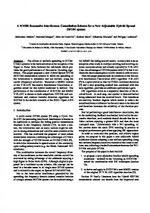
Fig. 17. Chip photo of 1-Gb DDR2 DRAM.
consumption of VNDS is less 5mA in 1-Gb DDR2 DRAM, which is small and acceptable for application. YI of column gate can be enabled after SAP1 enabled, which improves the tRCD parameter. The chip photo of the 1-Gb DDR2 DRAM is shown in Fig. 17, which has been evaluated the NDS effects for improving the sensing margin in low voltage and large Vtp offset voltage condition.
V. CONCLUSIONS Three novel circuit schemes are proposed to achieve sub 1.0V chip operation, low power consumption, and high performance in DRAM. Firstly, negatively-driven sensing (NDS) scheme enables sub-1.0V sensing operation without layout area penalty using negative voltage at SA region only. Secondly, special reference circuit with free-level precharged bitline (FLPB) scheme can remove the standby leakage current of WL-to-BL shortage fail in cell array region. Finally, the sense amplifier uses NDS offset cancellation control scheme. The performance of the NDS scheme has been verified through its realization on 1-Gb DDR2 DRAM chip.
REFERENCES [1] Masaki Tsukude, et al., “A 1.2-to 3.3-V Wide Voltage-Range/Low-Power DRAM with a ChargeTransfer Presensing Scheme,” IEEE J. Solid-State Circuits, vol. 32, pp. 1721-1727, Nov. 1997. [2] Jae-Yoon Sim, et al., “Charge-Transferred
Presensing, Negatively Precharged Word-Line, and Temperature-Insensitive Power-Up Schemes for Low-Voltage DRAMs,” IEEE J. Solid-State Circuits, vol. 39, pp. 694-703, April. 2004. [3] Goro Kitsukawa, et al., “256Mb DRAM Technologies for File Applications,” ISSCC, pp. 48-49, Feb. 1993. [4] Hee-Bok Kang, et al., A “Negatively-Driven Sensing (NDS) Scheme with Dual-Voltage Control for Sub-1.0V DRAM,” The 12th Korean Conference on Semiconductors, pp.43-44, Feb. 2005.
Hee-Bok Kang received the B.S. in 1988 and M.S. in 1990 and finished the doctor degree course in 19911996 and now is preparing the doctor’s thesis in electrical engineering at Korea University, Seoul, Korea. He joined LG Semiconductor in 1991 and now working for Hynix Semiconductor Inc., as a memory design engineer. He involved in DRAM and SRAM during 1991-1997 and in FeRAM since 1998, now in FeRAM embedded RFID tag, DRAM, FeRAM, and PRAM. His current interests are to develop DRAM related researches such as 1TFeRAM for the alternative next generation capacitor-less 1T-DRAM, FeRAM embedded system on a chip (SOC) and RFID tag, and next generation nonvolatile memories. Suk-Kyoung Hong is senior member of technical staff at Hynix Semiconductor Inc., Korea. Since 1997, He has worked for development of FeRAM and now PRAM. He received his BS in metallurgy in 1982 from Kookmin University, his MS in 1986 from Korea Advanced Institute of Science and Technology (KAIST) and his PhD in 1997 from Seoul National University, Korea, both in materials science and engineering. From 1986 to 1997, he worked as manager in thin film device at Samsung Electronics Co., Ltd., Korea.
JOURNAL OF SEMICONDUCTOR TECHNOLOGY AND SCIENCE, VOL.7, NO.2, JUNE, 2007
Heon-Yong Chang He joined Hyundai Electronics in 1997 and now working for Hynix Semiconductor Inc., as PRAM PI engineer. He has been involved in the development of DRAM. Currently, he is involved in the development of embedded-FeRAM RFID Tag (UHF) and PRAM. His current interest is to develop PRAM related research and development. Hae chan Park was born in Andong, Gyeongsangbuk-do, the Republic of Korea, 1974. He received the B.S degree in Physics from Chung-buk National University, Cheung-Ju, Korea, in 1993 and 2002, respectively. He has been with Hynix Semiconductor Company, Ltd., since 2002, where he has been involved in the development of 512-Mb DRAM. Currently, he is involved in the development of embedded-FeRAM RFID Tag (UHF) and nextgeneration new memory such as PRAM. Nam Kyun Park was born in YangYang, Kangwon-Do, Korea, in 1978. He received the B.S. degree in advanced materials science and engineering from Kangwon National University, Kangwon-Do, Korea, in 2003, and M.S. degrees from the Korea University, Seoul, Korea, in 2005, respectively. In 2005, he joined Hynix semiconductor Inc., Icheon-si, Korea, where he has been involved in the development of FeRAM. At present, he is involved in developing the next-generation memory, PRAM.
75
Man Young Sung He received the Ph.D. degrees in electrical engineering from Korea University in 1981.He is an IEEE member and a professor in Department of Electrical Engineering at Korea University. He is currently the president of Korea Institute of Electrical and Electronic Materials Engineers. Jin-Hong Ahn Jin-Hong Ahn was born in Busan, Korea, in 1958. He received the B.S. and M.S. degrees in electronic engineering from Seoul National University in 1982 and 1984, respectively. He joined GoldStar Semiconductor Co., Gumi Korea, in 1984. From 1986 to 1990, he was involved in designing SRAM's and mask ROM's. In 1991, he moved to the DRAM design group, Gold-Star Electron Co., Seoul Korea. From 1991 to 1998, he managed several generations of advanced DRAM design projects, 64Mb, 256Mb, MML and intelligent RAM. His interests in DRAM design during this time are new DRAM architectures, next generation DRAM circuit technologies, and low-cost DRAM design techniques. From 1999, he joined the memory R&D group, Hynix Semiconductor, Icheon, Korea, where he was engaged in the advanced memory design team. Now he is a technical director in Memory Design technology. Sung Joo Hong He joined Hyundai Electronics in 1992 and now working for Hynix Semiconductor Inc., in developing DRAM, PRAM and new advanced technology devices. He is currently vice president and leading the Device Division. His current interests are to develop DRAM, PRAM and new advanced technology devices related research and development.