A Software System for IEEE 1149.1 Boundary Scan Design, Simulation, and Demonstration A. Jutman, V. Rosin, R. Ubar Tallinn University of Technology, Raja 15, 12618 Tallinn, Estonia Email:
[email protected]
1. Introduction
Abstract In this paper, we describe a multi-functional software system, which provides a simulation, demonstration, and CAD environment for learning, research, and development related to IEEE 1149.1 Boundary Scan (BS) standard. The system supports important Boundary Scan data formats (BSDL, SVF) through which it can interact with other BS development tools. At the same time, the system provides a graphical design and simulation environment of BS-enabled chips and boards. It is also possible to simulate the behavior of various interconnect faults and automatically generate interconnect test patterns using one of many implemented algorithms. The system is based on a multiplatform JAVA environment and is publicly accessible over Internet as a freeware. Such combination of features is unique for a public domain BS software.
As long as printed circuit boards (PCB) will continue to exist, the PCB testing will remain a very important step in the production cycle of microelectronic systems. It has already become a mature research and engineering topic with well established standards and solutions the most important of which is the IEEE Std 1149.1 “Test Access Port and Boundary-Scan Architecture”, developed by Joint Test Action Group (JTAG) and balloted as a standard in 1990 [1]. The state of the art PCB testing is a mixture of Boundary Scan (BS), optical inspection, and in-circuit test with the latter seizing to exist. The BS seems to be the most universal and the only realistic low-cost solution, which besides manufacturing testing is used also in in-circuit programming and product maintenance.
Figure 1. Main window of the system
Table 1. Comparison of similar available systems Platform Usage Chip editing Board editing Fault diagnosis Various fault models Automatic TG Test programming Import/export Built-in help/tutorial Built-in examples Comes with HW
The BS applet Java web/local yes yes yes yes yes yes yes (BSDL, SVF) no/coming… many/extendable no
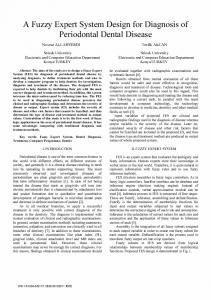
The current paper describes a multi-functional software system, developed in the first place for demonstration and simulation of different aspects of BS conception but also as a CAD environment for learning, research, and development related to IEEE 1149.1 standard. We show the advantages of our system over two other similar public domain systems. We also describe many important updates implemented since the last publication two years ago [2]. 2. System Overview The GUI window shown in Figure 1 should give a general impression about working modes of the teaching system. The window is basically divided into two parts: the Schematic View Panel and a set of control panels. The board under test is illustrated on the left side. It consists of BS-enabled chips connected into a single chain. In the Edit Board mode, the user can reconfigure the BS chain, remove chips, or add new from the library. In all other modes this panel illustrates active signals passing through interconnects and BS registers. The right-side panel allows switching between three basic working modes: TAP, Command, and Program modes, as the learning process goes on. The user normally starts with the TAP mode, which illustrates basic BS operating principles, and then passes through these modes ending up at the Programming mode used for advanced tasks of fault diagnosis. There are several other similar educational systems on Boundary Scan standard. The first one, called Scan Educator has been developed by Texas Instruments in the beginning of 90-s [3]. The second one is a recent development by a company called GÖPEL Electronic [4]. The functionality of both systems is rather limited compared to ours. This can be seen from Table 1. The most important element, which is missing in other systems, is the possibility of editing existing examples and creating own ones. Import/export capability allows for industrial BS-enabled ICs to be imported into the applet and then simulated. At the same time, created test programs can be exported using widely accepted by industry serial vector format (SVF). Another important difference is due to the fault insertion and fault modeling module, which enables real
ScanEducator DOS local no no no no no no no splendid few/fixed no
BScan Coach Windows local no no no no no no no nice/limited one/fixed yes
diagnostic tasks to be performed by students and, as the result, better learn interconnect fault models and fault detection and diagnosis methods. There are two features at which our system stands behind its counterparts. The first one is the availability of a built-in tutorial, which is quite an important part for an educational system. Therefore, we have intention to create it. The second feature is the educational hardware, a board which can be controlled by the system. We consider this part being not that important since usually such a hardware brings additional limitations and makes the system being less flexible. 3. Board Representation The Schematic View Panel (Fig. 2) comes with the schematic representation of the board layout. At the moment, possible elements of the board are restricted to chips themselves only. This means that only components which have BS structures can be represented and simulated in the applet. The BS standard distinguishes the following basic hardware elements: the Test Access Port, the TAP Controller, the Instruction Register, and a group of Test Data Registers, which in its turn consists of at least the Boundary Scan Register and the Bypass Register. All these structures are also illustrated in the Schematic View Panel. Illustration of a BS Chip. A BS chip is shown in the Schematic View Panel as a grey rectangle. According to the BS standard all the chips on the board are connected into a scan chain via TDI (Test Data In) and TDO (Test Data Out) pins. The white area inside the chip is the core logic, which is not illustrated in detail. The wrapper around the core logic is the Boundary Scan Register. It plays the role of separator between the logic circuitry and the I/O pins of the chip, providing internal control points for each pin. Each scan cell of this register consists of two flip-flops. One is used for capturing the state of the control point (the yellow one). Another one (the blue one) is needed for keeping the control value of the control point during the test mode. The control values and captured responses are shifted in and out in series via TDI and TDO pins.
Different colors highlighting different things are selected in the way making it easy to follow the simulation. Any change, when it happens can be quickly noticed. 4. Board and chip editing
Figure 2. Schematic View Panel The register at the very bottom of the chip is the Instruction Register (IR), the lower part (red) of which is used for holding the currently active instruction. The next instruction is shifted via the upper part of IR. After the instruction has been completely shifted in, the lower part is updated with the values from the upper part. The one-bit register right above the IR is the Bypass Register (BYR). It is usually used for faster test data shifting. The IR and the BYR are mandatory Test Data Registers (TDRs). There could be some optional design-specific TDRs in the BSDL description that are not normally shown upon the chip in the Schematic View Panel. The only optional TDR that is shown accordingly to the BSDL description is called the Device ID Register. There is a library of different chips and a number of built-in examples of various board schematics provided with our applet. So, the lecturer can select the most illustrative example for a particular topic. Signals and Wires. We use different colors for input pins as well. Ordinary data input pins are grey, while the control pins are red. By pushing the pins (the buttons) the user can drive a desired input line to either logic 0 or 1. Depending on the BSDL description for a particular chip the value 0 or 1 at a control input pin drives some of the outputs to the high impedance state. Each output which is not connected to any other chip, is supplied by an indicator, which shows the current state of the output line. There are four possible states for any signal line of the design. Logic 1 and logic 0 are indicated by green and blue colors correspondingly. The wires driven into the high impedance state are white. At the same time the output indicator holds value “Z”. If a wire is red and the indicator shows value “X”, then the logic value of the corresponding signal is unknown. The wire connecting all the TDIs and TDOs of all the chips together is always black. It is used for test data shifting in and out.
Our applet has a built-in BSDL parser which makes it possible for virtually any BS chip to be imported and simulated by our system. Moreover, the built-in simple board editor allows for any design to be created using arbitrary BS chips. We decided to do so, because it makes the work with the applet more exciting for a student. Even a test engineer may find some of the applet’s functionality useful for certain simpler tasks. The built-in BSDL parser became “smarter”, now it is possible to handle more than 120 common BSDL syntax faults with corresponding error message and exact fault position. The BSDL language is the standard for BS structures description. It provides the applet with information sufficient for simulation of most of the BS instructions. However, this format does not describe the internal functionality of the chip. Therefore, we have to use another format for this purpose. We have selected SSBDD (Structurally Synthesized Binary Decision Diagram) format [5] for its simplicity and efficiency. This format can be easily converted from a widely-used EDIF description by Turbo Tester software [6]. During the definition of a new chip, the user should provide both formats for complete description of the chip. However the SSBDD format may be omitted if there is no need to simulate the chip’s internal logic. We use our own very simple format for description of the interconnection between the chips. It consists of two parts: description of modules (chips) and description of connections (Fig. 3). In the Edit Board mode, the user can edit both parts by adding or removing some lines. The chips in “modules” section should come in the same order as they will be connected into the BS chain. They are separated by the sign “>”, which symbolically
Figure 3. Board Interconnect Description
the type of fault. This is done by selection of proper BS instructions and input test data. In the new version of the applet, the fault insertion and simulation module has been completely redesigned. Now the system makes clear difference between physical defects like opens or shorts and their modeling by stuckat and wiring faults. Different new modes of fault insertion have been implemented in the system (see Fig. 5).
Figure 4. Chip Library Viewer illustrates the ordering relation. Connections between chips can be created also by clicking upon corresponding pins with mouse pointer. Unneeded connections can be deleted in the same way. All the changes will be instantly reflected in the “connections” section of the interconnect description. There is a convenient Chip Library Viewer (Fig. 4), which can be used during the board design for better overview of available BS chips. It provides a good access to all the chips in the library. The user can simulate separate chips, delete, or edit them. The user can also add new chips to the library using this panel. 5. Simulation and Fault Diagnosis There are basically tree main simulation modes supported by the applet. They are: the TAP Controller mode, the Command mode, and the Program mode. In all modes there are two options: fault-free simulation and simulation for fault detection. The latter option implies that there is a certain faulty connection. Then the goal of simulation is to find this faulty connection and identify
Figure 5. Fault Insertion Module
The TAP Controller Mode. The TAP Controller simulation mode is illustrated in Fig. 1. In this mode, the user himself should take care of shifting in needed instructions and test data. Since, the Test Access Port consists of only TDI, TDO, TMS (Test Mode Select) and TCK (Test Clock) I/O pins, the task of the student becomes not quite trivial. All the instructions and test data can be shifted in via the TDI input only. The TAP Controller state together with an active instruction in the IR defines the operation and configuration of BS structures. For example, in order to select the EXTEST instruction, one should, first, reach the “Shift-IR” state of the TAP Controller starting from the “Test-LogicReset” and moving through the following states: “RunTest/Idle”, “Select-DR-Scan”, “Select-IR-Scan”, etc. These state transitions are made by changing the TMS value and applying the TCK. The second phase is to shift in a proper bit sequence, which corresponds to the EXTEST instruction. For example, it is either 00000000 or 10000000 for SN74BCT8244A. This information can be found from the Chip’s Commands sub-panel (see Fig.1). After that, when the chip is in the EXTEST state, the test data should be inserted into the Boundary Scan Register. This is done in the same manner, but in the “Shift-DR” state. As one can see the manipulation of a BS chip is quite a tricky task. Therefore, only a system, which allows instant simulation and illustration of all the student’s steps can help learning and easy finding all the mistakes and misunderstandings, which otherwise would likely be missed. The Command Mode. Students, once, become familiar with the TAP Controller operating modes and with the way different BS instructions work. They might want then to perform some time consuming operations automatically while concentrating on other aspects and applications of BS, such as, for instance, fault diagnosis. During fault diagnosis it is convenient to set up, at first, special operating modes for each chip and then to concentrate primarily on test vectors selection in order to detect and locate faulty lines. This is possible in a special BS simulation mode called the Command Mode. There is a list of available instructions for each chip. These instructions are defined in the BSDL description and could be different for different chips. The user just selects required instruction for each chip and defines the input data (Fig. 6). Usually, depending on the active instruction, the input data will be shifted into the Boundary Scan or Bypass Register. By pressing “Scan IR” button the user makes selected instructions active. He can press then “Scan DR” button and the input data
program that drives the TAP controller through desired states and applies a predefined sequence of vectors to the system under test. The test program is written in a standard SVF format and can be easily exported and used in other third party educational or commercial simulators or design tools. The system has also got an automatic test pattern generation module that generates test patterns (see Fig. 7) accordingly to all the major interconnect testing algorithms (counting, modified counting, true/ complement, interleaved true/complement, LaMa, walking one, walking zero). The test sequences can be applied in both ways: serially – through the scan chain and in parallel – through primary inputs. 6. Conclusions Figure 6. Command Mode Panel will be shifted in. At the same time the current state of Data Registers will be shifted out. It is a bit sequence which is shown in the Diagnostic Information sub-panel. For a certain test vector there is an expected output response. When the response is different from what was expected, the fault has been detected. It is possible to locate the faulty connection by analyzing the data in the Diagnostic Information sub-panel. In the Command mode there are two possible simulation options: slow animation mode and fast mode. The first one is intended for comprehensive illustration of various processes like shifting or switching taking place in the chip and different BS registers. The second mode is used for fast simulation without animation. It is useful when the primary goal is to get the diagnostic information. The Program Mode. The most advanced and automated mode of controlling your BS structures in the applet is the Program Mode. It allows user to write a test
In this article, we have described a multi-purpose system [2,7], which provides a simulation, demonstration, and CAD environment for learning, research, and development related to IEEE 1149.1 Boundary Scan standard. A BS device manipulation is quite a tricky exercise. Therefore, only a system, which allows instant simulation and illustration of all the user’s steps can help learning and easy finding all possible mistakes and misunderstandings, which otherwise would likely be missed out. Recently, the BS applet has become equipped with new working modes. They touch fault modeling, functional simulation, manual and automatic test vector generation, and import/export interface. The most important of all these improvements has to do with test generation and application. The system has also been supplied with a short introductory description, user manual, and dedicated exercises. Acknowledgements This work was supported partly by the Thuringian Ministry of Science, Research and Art (Germany), by the EU Framework V project REASON, and by the Estonian Science Foundation Grant No 5649. References [1] IEEE 1149.1-1990, “IEEE Standard Test Access
Port and Boundary-Scan Architecture,” 1990. [2] A. Jutman, A. Sudnitson, R. Ubar, “Web-Based
Training System for Teaching Principles of Boundary Scan Technique”, in Proc. 14th EAEEIE Conference, Gdansk, Poland, June 16-18, 2003. [3] Texas Instruments’ Scan Educator URL:
http://focus.ti.com/docs/toolsw/folders/print/scan_educator.html [4] GÖPEL Electronic Boundary Scan Coach URL:
http://www.goepel.com Figure 7. Program Mode Panel
[5] A.Jutman, J.Raik, R.Ubar, “SSBDDs: Advantageous
[6] Turbo Tester home page URL:
Model and Efficient Algorithms for Digital Circuit Modeling, Simulation & Test,” in Proc. of 5th Int. Workshop on Boolean Problems, Freiberg, Germany, Sept. 19-20, 2002, pp. 157-166.
http://www.pld.ttu.ee/tt/ [7] Boundary Scan Applet URL:
http://www.pld.ttu.ee/applets/bs