Web-Based Training System for Teaching Principles of Boundary Scan Technique A. Jutman, A. Sudnitson, R. Ubar Tallinn Technical University, Department of Computer Engineering Raja 15, 12618 Tallinn, Estonia Tel: +372 6202253, Fax: +372 6202253, Email:
[email protected].
Abstract A conception of training system for teaching IEEE 1149.1 Boundary Scan (BS) standard is presented. The system conforms to the idea of “Living Pictures” [2] where a tricky quite complicated content is represented in a graphical way and the student is provided with the possibility to “play” with the training system. The design/modification of BS structures inside the target chip; design/modification of the target board consisting of several chips; simulation of work of TAP controller, scan register and other BS registers; investigation of BS commands like EXTEST, BYPASS, etc.; insertion and diagnosis of interconnection faults – all these topics are supported by our teaching system. The system is implemented in a form of Java applet and can be freely accessed over Internet. The latter makes it easy for students even from foreign universities to use this system any time and in any place.
1. Introduction Until recently, most electronic systems consisted of one or multiple printed circuit boards (PCB), containing multiple integrated circuits (IC) each. Recent advances in IC design methods and technologies allow integration of these complex systems onto one single IC. These developments are driving engineers toward new System on a Chip (SoC)
design methodologies, which is seen as a major future direction for the semiconductor industry. The main test strategy for SoC is the IEEE P1500 “Standard for Embedded Core Test.” This standard has evolved from the earlier development in this area, namely, the IEEE Std 1149.1 “Test Access Port and Boundary-Scan Architecture”, which was created by Joint Test Action Group (JTAG) and aimed at testing PCBs. It is of no doubt that these new very important standards, especially the latter and the simpler one, have to be taught to future designers and test engineers. The “bed of nails”, was the main board test technique in 70s and 80s. It ensured the physical contact to any desired point of the circuitry. Modern PCBs, however, have a number of inaccessible internal layers as a rule, and the circuit packaging nowadays includes types like various “grid arrays” (PGA, BGA), which have a lot of inaccessible pins. These difficulties have led to introduction of the Boundary Scan standard. The BS architecture implies the insertion of scan chains in such a way, that each pin of each chip receives an internal control point. During the normal operation mode the scan cells are transparent, while in the test mode they provide with possibility of driving any of the control points to a desired value as well as catching the defects by reading the results of circuit operation. The standard defines also the Test Access Port (TAP) and the TAP Controller [1]. All these
14th EAEEIE conference, Gdansk, 2003 structures are quite complicated and hard to be taught in a traditional manner during a lecture. Therefore, new effective dynamic teaching concepts must be introduced. We apply the concept of “Living Pictures” [2] when building up our teaching system. The main features of such a system incorporate: graphical representation of the learning subject, dynamic content, user-friendly interface, concentration on the most important topics in the simplest possible way, set of various examples, easy action and reaction, and game-like style of learning. The same system could be used by teacher during a lecture when explaining the dynamic content as well as by students later at home when repeating and comprehending the topic. In this way this dynamic part of the lecture will not be lost. Moreover, the same system could be used during tests or examinations. Therefore, it must be easily available. How to keep up with all these requirements? The solution is to implement the system on the Java platform, which is supported by most operating systems, and put it into the Web. In the next section we give a general overview of our system and compare it with a similar system called ScanEducator from Texas Instruments [3]. The description of the PCB Panel together with BS registers comes in Section 3. In the section after we describe both TAP and Command modes of work with the applet. The final section of the article brings some conclusions.
2. System Overview We have selected the Java technology for our teaching system since it is well supported by main operating systems like Windows, Linux, and Solaris. Furthermore, Java allows for graphical content to be easily created. It also has well developed means for creating the user interface. We made our system available in the Web for free [4].
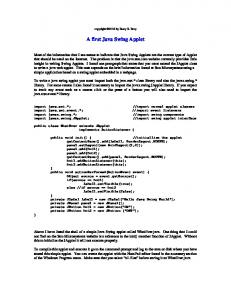
2 All the mentioned advantages of Java environment are at the same time the advantages of our teaching system against the ScanEducator [3] from Texas Instruments, which works under DOS only and must be installed locally instead of running over Internet. Another difference is that ScanEducator has only a couple of chips to work with, while our system is provided with a lot of built-in examples. We also decided to allow users to generate their own examples by creating a fully custom chip or board. Moreover, our applet has a possibility of specific fault insertion and its diagnosis. The applet (Fig. 1) allows several working modes: § design/editing of BS structures inside the target chip using the BSDL language [1]; § design/description of the target board that consists of several chips; § simulation of work of TAP Controller, scan register and other BS registers; § insertion and diagnosis of interconnecttion faults. In the Edit Board mode, each chip on the board can be defined and redefined. New chips can be also created and inserted. The applet reads the description of BS structures using BSDL format which is a part of the standard now. Such BSDL descriptions are widely available for free via Internet. This makes the work with the applet easier and more exciting, since the student can visualize the operation of many well known chips with BS available in the market. The latter may be interesting also for test engineers who need to check or debug their BS designs. At present, the only supported description of the chip’s internal logic is the SSBDD format [5]. However, this format is optional since for the simulation of the most BS operation modes the internal structure of the chip can be neglected. The simulation of the chip’s work can be done in two modes. The first one, the TAP Controller Mode, provides a very detailed illustration of operation of BS
14th EAEEIE conference, Gdansk, 2003
3
Figure 1. Applet main window registers and the TAP controller. This mode is intended for the beginners and for teachers, helping to understand all the needed basics. Another mode, the Command Mode, can be used for faster simulation of BS commands like EXTEST, SAMPLE/PRELOAD, etc. with different predefined input data. The same mode is useful for the fault diagnosis. There is a possibility of random or specific fault insertion. The operation of the faulty device can be then simulated and the fault can be diagnosed.
3. PCB Representation and Editing The PCB Panel (Fig. 1) comes with the schematic representation of the PCB layout. At the moment, possible elements of PCB are restricted to chips themselves only. This means that only components which have BS structures can be represented and simulated in the applet.
The BS standard distinguishes the following basic hardware elements: the Test Access Port, the TAP Controller, the Instruction Register, and a group of Test Data Registers, which in its turn consists of at least the Boundary Scan Register and the Bypass Register. All these structures are also illustrated in the PCB Panel.
3.1. Representation of a Chip A BS chip is shown in the PCB Panel as a grey rectangle. According to the BS standard all the chips on the board are connected into a scan chain via TDI (Test Data In) and TDO (Test Data Out) pins. The white area inside the chip is the core logic, which is not illustrated in detail. The wrapper around the core logic is the Boundary Scan Register. It plays the role of separator between the logic circuitry and the I/O pins of the chip, providing internal control points for each pin. Each scan cell of this register consists of two
14th EAEEIE conference, Gdansk, 2003 flip-flops. One is used for capturing the state of the control point (the yellow one). Another one (the blue one) is needed for keeping the control value of the control point during the test mode. The control values and captured responses are shifted in and out in series via TDI and TDO pins. The register at the very bottom of the chip is the Instruction Register (IR), the lower part (red) of which is used for holding the currently active instruction. The next instruction is shifted in via the upper part of IR. After the instruction has been completely shifted in, the lower part is updated with the values from the upper part. The one-bit register right above the IR is the Bypass Register (BR). It is usually used for faster test data shifting. The IR and the BR are mandatory Test Data Registers (TDRs). There could be some optional designspecific TDRs in the BSDL description that are not normally shown upon the chip in the PCB Panel. The only optional TDR that is shown accordingly to the BSDL description is called the Device ID Register. There is a library of different chips and a number of built-in examples of various PCB layouts provided with our applet. So, the teacher can select the most illustrative example for a particular topic.
3.2. Signals and Wires We use different colors for input pins of different functionality. Ordinary data input pins are grey, while the control pins are red. By pushing the pins (the buttons) the user can drive a desired input line to either logic 0 or 1. Depending on the BSDL description for a particular chip the value 0 or 1 at a control input pin drives some of the outputs to the high impedance state. Each output which is not connected to any other chip, is supplied by an indicator, which shows the current state of the output line. There are four possible states for any signal line of the design. Logic 1 and logic 0 are indicated by green and
4 blue colors correspondingly. The wires driven into the high impedance state are white. At the same time the output indicator holds value “Z”. If a wire is red and the indicator shows value “X”, then the logic value of the corresponding signal is unknown. The wire connecting all the TDIs and TDOs of all the chips together is always black. It is used for test data shifting inside and outside. Different colors highlighting different things are selected in the way making it easy to follow the simulation. Any change, when it happens can be quickly noticed.
3.2. PCB and Chip Editing Our applet has a built-in BSDL parser which makes it possible for virtually any BS chip to be imported and simulated by our system. Moreover, the built-in simple PCB editor allows for any design to be created using arbitrary BS chips. We decided to do so, because it makes the work with the applet more exciting for a student. Even a test engineer may find some of the applet’s functionality useful for certain simpler tasks. The user can select either one of builtin examples to be modified or he can start with an empty design to build everything from scratch. The BSDL language is the standard for BS structures description. It provides the applet with information sufficient for simulation of most of the BS instructions. However, this format does not describe the internal functionality of the chip. Therefore, we have to use another format for this purpose. We have selected SSBDD (Structurally Synthesized Binary Decision Diagram) format [5] for its simplicity and efficiency. This format can be easily converted from a widely-used EDIF description by Turbo Tester software [6]. During the definition of a new chip, the user should provide both formats for complete description of the chip. However the SSBDD format may be omitted if there
14th EAEEIE conference, Gdansk, 2003 is no need to simulate the chip’s internal logic. The board consisting of several chips can be also edited or modified. Connections between chips can be created by clicking upon corresponding pins with mouse pointer. Unneeded connections can be deleted in the same way.
4. Simulation and Fault Diagnosis There are basically two main simulation modes supported by the applet. They are: the TAP Controller mode and the Command mode. In both modes, there are two options: fault-free simulation and simulation for fault detection. The latter option implies that there is a certain faulty connection. Then the goal of simulation is to find that faulty connection and identify the type of fault. This is done by selection of proper BS instructions and input test data. There are basically two possible types of faults available up to now: stuckat 0 and stuck-at 1. We are also going to implement other faults like shorts between adjacent lines or broken connections.
4.1. The TAP Controller Mode The TAP Controller simulation mode is illustrated in Fig. 1. In this mode, the user himself should take care of shifting in needed instructions and test data. Since, the Test Access Port consists of only TDI, TDO, TMS (Test Mode Select) and TCK (Test Clock) I/O pins, the task of the student becomes not quite trivial. All the instructions and test data can be shifted in via the TDI input only. The TAP Controller state together with an active instruction in the IR defines the operation and configuration of BS structures. For example, in order to select the EXTEST instruction, one should, first, reach Shift-IR state of the TAP Controller starting from the Test-Logic-Reset and moving through the following states: Run-Test/Idle, SelectDR-Scan, Select-IR-Scan, etc. These state transitions are made by changing the TMS value and applying the TCK. The
5 second phase is to shift in a proper bit sequence, which corresponds to the EXTEST instruction and shown in Chip’s Commands sub-panel (see Fig.1). After that, when the chip is in the EXTEST state, the test data should be inserted into the Boundary Scan Register. This is done in the same manner, but in the “Shift-DR” state. As one can see the manipulation of a BS chip is quite a tricky task. Therefore, only a system, which allows instant simulation and illustration of all the student’s steps can help learning and easy finding all the mistakes and misunderstandings, which otherwise would likely be missed.
4.2. The Command Mode Students, once, become familiar with the TAP Controller operating modes and learn how different BS instructions work. They may want then to perform some time consuming operations automatically while concentrating on other aspects and applications of BS like, for instance, fault diagnosis. During fault diagnosis it is convenient to set up, at first, a special operating mode for each chip and then to concentrate primarily on test vectors selection in order to detect and locate faulty lines. This is possible in a special BS simulation mode of our applet called the Command Mode. There is a list of available instructions for each chip. Those instructions are defined in the BSDL description and could be different for different chips. The user just selects its own instruction for each chip and defines the input data (Fig. 2). Depending on the active instruction, the input data will be shifted into the Boundary Scan Register or other registers. By pressing “Scan IR” button the user makes selected instructions active. He can press then “Scan DR” button and the input data will be shifted in. At the same time the current state of Data Registers will be shifted out in a form of bit sequence which
14th EAEEIE conference, Gdansk, 2003 is shown in Diagnostic Information subpanel. When the output response is different from what was expected, the fault has been detected. It is possible to locate the faulty connection by analyzing the data in the Diagnostic Information sub-panel.
6 illustration of all the student’s steps can help learning and easy finding all possible mistakes and misunderstandings, which otherwise would likely be missed out. The system consists of several interactive modules and supports the possibility of distance learning as well as a web-based computer-aided teaching. The interactive modules are focused on easy action and reaction, learning by doing, a game-like use, and encourage students for critical thinking, problem solving, and creativity.
6. Acknowledgments
Figure 2. Instruction Selection Panel In the Command mode there are two possible simulation options: slow animation mode and fast mode. The first one is intended for comprehensive illustration of various processes like shifting or switching taking place in the chip and different BS registers. The second mode is used for fast simulation without animation. It is useful when the primary goal is to get the diagnostic information.
This work is supported by the Thuringian Ministry of Science, Research and Art (Germany), by EU V Framework project REASON, and by the Estonian Science Foundation (grants No 4876 and 4300). We also thank Ruslan Gorjachev and Vjatseslav Rosin for the perfect implementation of our ideas in the form of Java applet.
References [1] H. Bleeker, P. van den Eijnden, F. de Jong,
Boundary-Scan Test: A Practical Approach. Kluwer Academic Publishers, Dordrecht, the Netherlands, 1993. [2] H.-D. Wuttke, K. Henke, “Teaching Digital
Design with Tool-Oriented Learning Modules nd “Living Pictures”, in Proc. of 32 ASEE/IEEE Frontiers in Education Conference, Boston, USA, Nov. 6 - 9, 2002, Session S4G, pp. 25-30.
5. Conclusions
[3] Texas Instruments’ Scan Educator URL:
In this article, we have described a teaching system [4], which is developed in order to make learning of the IEEE Std 1149.1 “Test Access Port and BoundaryScan Architecture” standard an easy task. A BS device manipulation is quite a tricky exercise. Therefore, only a system, which allows instant simulation and
[4] Teaching system URL:
http://www.ti.com/sc/data/jtag/scanedu.exe http://www.pld.ttu.ee/dildis/automata/applets/bs/ [5] A. Jutman, J. Raik, R. Ubar, “SSBDDs: Advan-
tageous Model and Efficient Algorithms for Digital th Circuit Modeling, Simulation & Test,” in Proc. 5 Intl. Workshop on Boolean Problems, Freiberg, Germany, Sept. 19-20, 2002, pp. 157-166. [6] Turbo Tester home page URL: http://www.pld.ttu.ee