tecture makes heavy use of the techniques of bit serial ... that multiplication of real values may be achieved us- ... A block diagram of the basic layout of a group of ..... Binomial Threshold Distribution (mean 7) .... tors ( 2n ?1] bits) is that the shift register polynomial ..... 11] N. Zierler, \Primitive trinomials whose degree is.
A stochastic neural architecture that exploits dynamically recon gurable FPGAs Max van Daalen, Peter Jeavons and John Shawe-Taylor, Connection Science and Machine Learning Group, Department of Computer Science, Royal Holloway University of London, Egham, Surrey TW20 0EX, United Kingdom
Abstract In this paper we present an expandable digital architecture that provides an e�cient real time implementation platform for large neural networks. The architecture makes heavy use of the techniques of bit serial stochastic computing to carry out the large number of required parallel synaptic calculations. In this design all real valued quantities are encoded on to stochastic bit streams in which the `1' density is proportional to the given quantity. The actual digital circuitry is simple and highly regular thus allowing very e�cient space usage of ne grained FPGAs. Another feature of the design is that the large number of weights required by a neural network are generated by circuitry tailored to each of their speci c values, thus saving valuable cells. Whenever one of these values is required to change, the appropriate circuitry must be dynamically recon gured. This may always be achieved in a xed and minimum number of cells for a given bit stream resolution.
1 Introduction One of the major constraints on hardware implementations of neural networks [1, 2], is the amount of circuitry required to perform the multiplication of each input by its correspsonding weight. This problem is especially acute in digital designs, where parallel multipliers are extremely expensive in terms of circuitry. Adopting an equivalent bit serial architecture, signi cantly reduces this complexity, but still tends to result in large and complex overall designs. A single such multiplier would consume a signi cant proportion of a current state of the art FPGA, thus making the use of such devices impractical for this approach.
This paper describes an alternative neural network architecture which may be implemented using standard VLSI technology, but also maps extremely e�ciently to dynamically recon gurable FPGAs [3]. The central idea is to represent the real-valued signals passing between neurons using stochastic binary sequences. In order to represent a real value of v, in the range [?1; 1], we use a stochastic sequence in which the probability of each bit being set to one is (v + 1) =2. Given two independent bit sequences of this type, representing two real values, the sequence obtained by calculating the exclusive-or of the two bit streams will represent the product of the two values. This means that multiplication of real values may be achieved using very simple logic circuitry: a single XOR gate. The circuitry used to generate the proposed stochastic bit streams is highly pipelined and thus potentially extremely fast [4]. The individual pipeline stages, known as modulators are simple, and the number used de nes the overall resolution of the generated bit stream. The approach taken is to synthesize the required stochastic bit stream by appropriately combining many independent stochastic bit streams with a bit probability of one half [6]. These xed value bit streams, referred to as carrier streams, are easy to generate using linear feedback shift registers [5, 4], as described later. The use of stochastic bit streams also enables each neuron to calculate a suitable activation function using very simple circuitry. In fact, the activation function is obtained by using the interaction of the probability distribution of the input bits, and the probability distribution of a threshold value, in the following way: the weighted input bits to each neuron are summed using a simple counter and the nal total is compared to a preloaded threshold value. The result of this comparison determines the output of the neuron, which is
a single bit forming part of a stochastic bit stream representing the result of the activation function. With this simple circuitry, various di�erent activation functions can be obtained depending on the choice of the probability distribution for the threshold value. For example, a linear activation function may be obtained by using a uniform probability distribution for the threshold value, a sigmoid activation function may be obtained by using an impulse-function probability distribution for the threshold value. A detailed analysis of these results is presented in [7]. Another of the problems facing VLSI neural networks is the high degree of connectivity between individual neurons. The use of stochastic bit streams and time division multiplexing has made it possible to design a neuron that behaves as if it has many inputs from other neurons, but in fact has only one physical connection. For this reason, the physical connectivity between the neurons in the design we propose is very straight forward. This allows the number of neurons per device to be very high, as they can be e�ciently packed in tightly spaced regular structures, with a minimum of global wiring. These factors are very important when FPGAs are to be used as the hardware implementation platform, as both the macro cells and the limited amount of global wiring can be e�ciently allocated. As in all applications of stochastic computing, the design allows a exible tradeo� between speed and precision because the precision of the output may be increased by processing more bits [8]. The most significant aspect of the design, with regard to the overall speed of operation, is that it readily allows successive layers of a network to be pipelined. This means that very large networks may be constructed by cascading several single or multi-layer chips, and the throughput rate will be independent of the total number of layers. The purpose of this paper is to describe the overall architecture of the proposed design and show how it may be e�ciently mapped to dynamically recon gurable FPGAs, and thus used to implement standard neuron models. A possible learning algorithm for a neural network of this type is described in [7]. We begin by describing the overall architecture of the type of neural network described by this paper, and explain the techniques used to allow the individual neurons to be fully connected. We then describe the detailed operation of an idividual neuron, including a detailed explanation of the novel statistical technique used to generate an appropriate activation function. Finally, we present details of the design for the novel circuitry used to generate the large number of real val-
ued stochastic bit streams, and describe experimental results obtained from simulations.
2 The Overall Network Architecture A block diagram of the basic layout of a group of neurons on an FPGA, all sharing the same input, is illustrated in Figure 1. Depending on the size of the package available, there may be several such groups accomodated on a single FPGA. Associated with each bit arriving on the shared input line to each neuron, there is a unique weight bit. The stochastic values representing the values of these weights are generated either o�-chip, or on-chip by the circuitry described later in this paper. One bit from each of the streams representing the weights is distributed to each neuron via the shift register elements labelled w , drawn down the right hand side of Figure 1. n
T
in
W
Q
in
? a � n
? a � 3
? a � 2
? a � ? Q 1
neuron
neuron neuron neuron
� w? �
in
n
� w? � � w? � � � w? � 3
2
input
1
out
Figure 1: Layout of a group of neurons within a chip Each neuron also has associated with it a section of another shift register, that is used to load it with a threshold value. The input line to this shift register is labelled T in Figure 1, and the connections between successive sections are indicated by the links between successive neurons. The threshold values, which are represented as normal binary integers, are loaded into in
this shift register whenever the neuronal thresholds are updated. The loading of threshold values is performed by the external support circuitry, and may be carried out in parallel with the loading of weight bits. For each input bit arriving at the group of neurons, the weight shift register W has to be completely loaded with the appropriate bits, one for each neuron in the group. This shift register is therefore the fastest operating circuit element within the design, so it is important that it is operated at the maximum possible speed. The loading time for this shift register ultimately determines the overall speed of the device. To maximise this, this shift register can be split up into sections, allowing them to be loaded in parallel. This does however soak up additional pins on the device, and make the external housekeeping circuitry more complicated, so some compromise must be reached. In order to explain the way in which the input signals themselves are organised we shall assume that the neurons are con gured as a fully-connected multilayer feed-forward network, as illustrated in Figure 2. The group of neurons shown in Figure 1 will form a single layer within this network. The other layers will be formed from similar groups of neurons, either on the same device or another device.
P r o c e s s i n g
d i r e c t i o n
?
I1
I2
I3
I4
I5
O1
O2
O3
O4
O5
@HPX?HPX�?HPX�HP @PX�?�HPPX��?�HPX���H @PX����HP���?��H���@?���?��� �?���@��@���m �?HP�?@HPX@HPPXm ?HPX@HPXH@PXmLayer 1 �?H���@H��H@P�m ��m �HPX���H ��H���@���?��� � � ? ? H @HPX?@HPX�?HPX��HP @HPX��?�HP @ � X � � P � P� HPX��?@HPX�PXHPX?@H �?�����@��m �?��@H��H@P�m ��m �? P@HPm ? PXH@PXmLayer 2 �HPX���H �HP��?��H���@���?��� � ? @HPX?@HPX�?HPX��HP @HPX��?�HP @ X � � P � P � HPX�?@HPX�PXHPX?@HPX �? @HPm �?�����@��m �?��@H��H@P�m ? H@PXmLayer 3 ��m
Figure 2: A fully connected multilayer network In order for each neuron to be connected to all the neurons in the previous layer the stochastic bit streams, representing the real valued outputs of the neurons in this previous layer, are time multiplexed on to one physical input. (In the case of the rst layer
in the network, it is the network inputs which are multiplexed.) The time multiplexing is arranged so that one bit from each of the appropriate bit streams is presented in turn. When the neuron has processed one bit from each of the time multiplexed stochastic input streams, together with one bit corresponding to each weight, it produces one bit of its stochastic output stream. The details of the internal processing to compute this output bit are dealt with in the next section. The output bit produced by each neuron is passed to another shift register, constructed from elements labeled a , and shown on the left hand side of Figure 1. Using this shift register the results may be clocked out and passed to the next layer of the network. It is important to note that on every neural cycle, each neuron produces only one bit. This bit is then latched and transfered to the next layer, via the a shift register, whilst the original neuron processes the next bits of the mutiplexed input bit streams. The serial output of this shift register, Q , automatically produces input bits for the next layer in the correct time multiplexed format. In this architecture the number of logical inputs to a particular neuron will be equal to the number of neurons in each layer. Taking the network illustrated in Figure 2 as an example, there are ve neurons in each layer, so in the implementation we have described each neuron will receive ve sequential logical inputs. The number of neurons in a layer may be increased very simply by combining groups of neurons together and passing the same input stream to all of them. The output shift registers from all the groups that have been combined may be simply joined together and will still contain the correct sequence of bits to be passed to the next layer. The number of logical interconnections in the fully-connected network increases with the square of the number of neurons in each layer, but because of the high degree of parallelism the speed of operation of the physical device decreases only linearly with the size of each layer. The operating speed is in fact independent of the number of layers used, although additional layers will contribute to a pipeline delay through the network. This means that very large networks of neurons can be constructed using the hardware we describe whilst maintaining a high processing speed. The nal output bit streams, produced by the neurons in the last layer must be converted back into real values. This is easily done by counting the ones in the given frame of output bits with a fast binary counter. The real valued answer is then calculated by dividing i
out
the accumulated count by the total number of bits in the output stream. This task would be carried out by the external support circuitry.
o
In this section we describe a single digital stochastic neuron with n logical inputs, as illustrated in Figure 3. The operation of the two shift register elements, SR and SR which conduct the weights to the neuron and then carry away the result, have already been discussed in the previous section. The neuron has one physical input line along which it receives, successively, during a single operational cycle, a single bit from each of the n sequences representing its input values. During the same operational cycle, the neuron also receives a single bit from each of the sequences representing the corresponding n weight values. These bits are made available by the weight shift register element SR . a
w
Q
T I W
in
in
in
S
o
T shift
S
i
????????
in
�
D - - - - - -D0 counter Q count n
?
SR Q
a
n
�
? ?
out
T
next
o
p = p1 (1 ? p2 ) + p2 (1 ? p1)
3 The Stochastic Neuron
w
To explain its operation, consider a two input XOR gate with stochastic inputs p1 and p2, and a stochastic output p . The Exclusive-OR function de nes that,
6
?
SR I
w
? ?
next
W
out
Figure 3: The elements of a stochastic neuron The rst step in the processing is to multiply each input value by the corresponding weight value to obtain a weighted input value. The multiplication of the input bit by the weight bit is carried out by the single XOR gate shown in Figure 3. This simple multiplication operation is one of the primary advantages of the use of stochastic computing, as mentioned in the introduction.
In order to represent real values v1 and v2 , in the range [?1; 1] the values p1 and p2 become (v1 + 1)=2 and (v2 + 1)=2. By substituting into the above equation for p we get, p = 21 ? 21 v1v2 Finally the value p must be considered in the range [?1; 1], this is achieved by applying the transformation v = 2p ? 1, giving, o
o
o
o
o
v = ?v1 v2 o
This is in fact the negative product of the two input values, so in order to ensure that the output has the correct polarity, either the external weight values must be complemented, or an Exclusive-NOR gate could be used. The rst option can be carried out at no extra cost in terms of circuitry, and is therefore preferable. The next phase of the processing is to sum the weighted inputs using a counter. The value accumulated in the counter from all the weighted inputs is then compared against the threshold in order to produce an output bit. To reduce the circuitry required we do not in fact do the comparison directly, instead we use an appropriate value to initially o�set the counter. This value is passed to the neuron by the T threshold shift register, shown in Figure 3. The o�set value is chosen so that the counter will over ow into its top bit if the chosen threshold is exceeded. The output of the neuron may then simply be taken from the most signi cant bit of the counter, this is then connected to the answer shift register element SR . Once the output bit has been obtained the counter is reset to the required o�set value and the entire operational cycle repeats for the next bits of the n sequences representing the weighted input values. a
4 The output threshold function In order to calculate the value represented by the output sequence from a digital stochastic neuron we must calculate the probability that the output bit takes the value one. If this probability is p, then the sequence output from the neuron will represent the value 2p ? 1.
We now obtain an expression for this probability p by considering the probability distribution of the input values and the threshold value. Each input value will contribute 0 or 1 to the counter, on each operational cycle, as described above. Hence, the total net input contribution to the counter, after summing the contributions due to all of the n inputs to the neuron, will be an integer between 0 and n. The probability function for this total will be denoted by . We will set the threshold value to be an integer in the range 0 to n ? 1, chosen according to some probability function. This probability function will be denoted by �, and may be varied according to the neuronal behaviour desired, as described below. For notational convienience, we choose a numbering for all neurons and refer to each neuron by its number. The set of all possible neural connections will be labeled E , and for a connection (i; j ) 2 E we denote the associated weight value by w . For the purposes of this paper we will assume throughout that if neuron i is connected to neuron j then j > i. Such a numbering can always be found provided the network is cycle free. This is the feedforward condition on the connectivity. A neuron will output a one if the total in the counter exceeds the threshold value. Hence, the probability, p, that the digital stochastic neuron outputs a one, is given by: ji
p=
X
(j )�(k)
j>k
To demonstrate the e�ect of varying the distribution � we will rst examine two special cases:
Uniformly distributed threshold value The rst will be to take a uniform probability distribution for the threshold number:
�(k) = 1=n; k = 0; : : :; n ? 1 In this case the probability, p, that the output bit is set to one is X X (j )(j=n) = (1=n) j (j ) p= n
n
j =1
j =1
The last sum is just the expected value of the counter input. Now this counter input is the sum of n independent variables, each consisting of a single bit from a stochastic binary sequence representing a weighted input value, as described above. Using the
above terminology, if we assume that the neuron we are analysing is neuron i then the weighted input from neuron j is o w . Since there are n inputs to neuron i, after each complete operational cycle the counter value is the sum of n independent variables which have means (o w + 1)=2. This P means that the expected value of the counter is ( )2 (o w + 1)=2, giving: j
j
ji
ji
i;j
X
p = (1=n)
2
j :(i;j )
j
E
ji
(o w + 1)=2 j
ji
E
The value represented by the output sequence is therefore:
X
o = (1=n)
2
j :(i;j )
ow j
ji
E
This choice of � therefore achieves a linear activation function.
A single threshold value The second special case we consider is where all of � is concentrated on one value, k0 : � if k = k0 �(k) = 1; 0; otherwise In this case the probability, p, that the output is equal to one is the probability that the total net input contribution to the counter is greater than k0, which is a function of k0:
p=
X n
(j )
j =k0 +1
So, in this case p is equal to the \probability distribution function" of the counter value. This counter value is the sum of independent contributions from each input, so with a large number of inputs its probability distribution function will have a sigmoid shape. This is a consequence of the central limit theorem [10]. Since the value o represented by the output sequence is a linear function of p, this choice of � achieves a sigmoid activation function. Numerical simulation indicates that a digital stochastic neuron with 15 inputs will in fact have a reasonably smooth sigmoid activation function when the threshold value is chosen in this way.
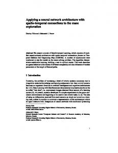
1.0
above. Hence the variability of the sequence, and the number of bits required to estimate the value which it represents to a given degree of accuracy, depends only on the value of this probability. Thus the neural processing described above does not cause any systematic increase in the variability of the stochastic sequences used in this design.
0.8
5 Generating stochastic bit streams
Output Probability
Uniform Threshold Distribution (0-14) Single Valued Threshold Distribution (7) Binomial Threshold Distribution (mean 7)
0.6
0.4
0.2
0.0 0.0
0.2
0.4 0.6 Input Probability
0.8
1.0
Figure 4: Activation functions (15 equal inputs) Figure 4 shows the activation functions resulting from these special choices of �. The graph shows the probability of the output bit being set to one on each operational cycle, as a function of the probability that each bit in the weighted input sequences is set to one, for a digital stochastic neuron with 15 equal inputs. The sigmoid activation function shown in Figure 4 for the single-valued threshold distribution is obtained by setting a xed threshold value of 7. In general the probability function � may be chosen to lie between the two extremes outlined above. For example, � may be a binomial distribution for n ? 1 trials with mean m 2 [0; n ? 1]. Figure 4 shows the activation function obtained by choosing � to be a binomial distribution for 14 trials with a mean of 7. The fact that this distribution gives rise to an activation function which is intermediate between the two cases considered above may be seen by comparing the three activation functions shown in Figure 4. The output from the neuron is a stochastic sequence which may be used as an input to other neurons or used to estimate the corresponding real value. It is important to note that each bit of the output sequence is calculated independently with the probability derived
The large numbers of independent stochastic bit streams representing the real-valued inputs to the neurons and weight values may be generated very simply using FPGA technology, as we now describe. The stochastic bit stream generators synthesize the required output bit streams, by appropriately combining many independent stochastic bit streams with a bit probability of one half [6]. These xed value bit streams, referred to as carrier streams, are described later. A given stochastic bit stream generator is constructed as a pipeline of k series connected single bit modulators, one for each bit of resolution in the required probability value. The input consists of a k bit binary value, representing a probability in the range 02 to 0:1111 : : : 1112. The individual k binary bits of this value will be called \modulation bits", and are used to download a series of k `1' or `0' bit modulators to the FPGA.
5.1 The bit modulator The circuit diagrams below (Figure 5 and Figure 6) shows the logic required to implement the respective bit modulators. Each bit modulator processes a bit stream from the preceding stage (the very rst stage is supplied with an all zero stream of bits) according to the value of the corresponding modulation bit which in turn de nes the actual circuit downloaded to the FPGA.
stage(n?1)
a
a
clock
a
FF
a stage
(n+1)
Carrier input Figure 5: Bit 1 modulator element The output of a given bit modulator is connected to a clocked ip op which allows these devices to be
cascaded in series, thus forming a pipeline, producing one new output bit with every clock cycle.
stage(n?1)
a
a
clock
a
FF
5.2 Bit stream resolution All modulators multiply their input bit streams by . A consequence of this is that in a given stream generator each modulator acquires a particular weighting factor with respect to the nal output stream. The k modulator, that is also the one furthest from the nal output, has the smallest weighting factor. This then de nes the resolution of a k modulator bit stream generator as being 21k . To accurately represent a value as a stochastic bit stream of this type, it is important that the appropriate number of stream bits are processed such that any inaccuracies due to random variance errors are eliminated. As the bit stream is a Bernoulli sequence, its variance takes the form of a binomial distribution, and is a function of the encoded bit probability. The worst case variance occurs when p = 21 , and it can be shown that the number of stream bits required to achieve an acceptable level of accuracy is given by the following expression: n = 22 ?2, where v is the number of bits in the binary probability value. 1 2
a stage
(n+1)
Carrier input Figure 6: Bit 0 modulator element The particular logic operation implemented by a bit modulator depends on its type. A `1' bit modulator calculates the bit-wise OR of the input stream and the carrier stream, whilst a `0' bit modulator calculates the bit-wise AND of the input stream and the carrier stream. Thus very e�cient usage of electrically recon gurable FPGAs is possible [3], as the required binary probability value is directly encoded into the stream generator as a series of `1' or `0' bit modulators. To change this probability value, the relevant part of the FPGA is rapidly recon gured. To understand the e�ect of each modulator on how the overall stream generator works, consider the probability of a bit being set in the output of a particular modulator on any clock cycle when the probability of a bit being set in the input stream from the previous stage is p. If the modulator is of type `1', then it follows from the independence of the input stream and the carrier stream that the probability of the output bit being set is 21 p + 21 . On the other hand, if the modulator is of type `0', then the probability of the output bit being set is 12 p. The combined e�ect of the appropriate sequence of modulators, is to construct a bit stream in which the probability of a bit being set is equal to the original de ning k bit probability value [6]. Note that a full or semi-custom VLSI implementation would require the use of generalised bit modulators to construct programmable bit stream generators. These devices would have an additional input to select the appropriate functionality of the bit modulator. These modulation inputs would be connected, in sequence, to one of k input bits representing the required binary probability value. The k input bits would be stored in a local holding register. For further details see [4]. Bit stream generators that are intended to generate xed stochastic values may be e�ciently implemented in the manner described for FPGAs, but would not be recon gurable. Furthermore, the holding register for the k bit probability value would not be required.
th
v
5.3 Generating the carrier streams A chip containing n, k modulator, bit stream generators will require kn statistically independent carrier streams. Ideally each stream should each be based on a truly random source of bits, but this is di�cult to arrange and thus impractical within a digital device. Register length 17 31 89 127 337 521 607 1279 2281 3217 4423 9689
Possible tap positions 3, 5, 6 3, 6, 7, 13 38 1, 7, 15, 30, 63 55 32, 48, 158, 168 105, 147, 273 216, 418 715, 915, 1029 67, 576 271, 369, 370, 649, 1393, 1419, 2098 84, 471, 1836, 2444, 4187
Table 1: Taps for maximal length PRBS The solution described in this paper is to make use of a linear feedback shift register, con gured to generate a maximal length pseudo random bit sequence [9]. The criterion for maximal length PRBS generators ([2 ? 1] bits) is that the shift register polynomial n
of degree n must be primitive over the Galois eld of order 2. Table 1 gives a selection of useful register sizes and tap positions that lead to such sequences. More details, and further tables of shift register tap positions are given in [9, 11].
Multiple streams from a small number of taps One solution to the problem of generating many independent sequences has been described by [5], here a single large PRBS generator is used. The multiple carrier streams are all derived from it by adding (modulo 2 addition) together in di�erent combinations the outputs from a small number of taps taken from appropriate points along the shift register. These distinct carrier streams, are each part of the main pseudo random sequence, but shifted so that they start from di�erent positions. This follows from the fact that if two sequences (s ) and (t ) satisfy the generator with polynomial i
i
p(x) = x + n
?1 X
n
c x + 1; i
i
i=2
then the stream (r = s � t ) also satis es the same polynomial i
r+ j
n
�
?1 M
n
i
i
!
c r + �r i
i=2
= s+ � j
n
j
i
j
!
?1 M n
c s + �s =2 ! ?1 M c t + �t � i
j
j
n
n
= 0�0= 0
i
j
i
j
i=2
It is suggested in [5] that to minimise unwanted correlations between the derived streams the tap positions and combinations used to produce them should be organised in such a way that the resulting sequences start from well-spaced locations in the original sequence. However, it should be noted that this is not su�cient to ensure that the derived sequences are not highly correlated. In fact, if the number of derived sequences is greater than the number of taps then this method is bound to introduce correlations between them. To illustrate this point consider using just two tap positions yielding two sequences, (s ) and (t ), and i
i
i
i
i
i
Multiple streams from successive taps The method presented in this paper for generating the carrier streams also makes use of a single maximal length PRBS generator. The streams are simply obtained directly by tapping successive elements of the PRBS shift register. These bit streams are highly overlapping, but almost perfectly uncorrelated [6]. Any realistic device will require a large number of carrier streams, such that typical shift register lengths will be of the order of 1000 bits (lengths of this order will also produce extremely long PRBS sequences). Such a shift register would be sectioned up, with each portion supplying carrier streams to the local stream generators. In this way a large PRBS shift register can be conveniently and e�ciently distributed across a chip. In order to ensure that the carrier stream inputs to successive modulators in a bit stream generator do not coincide we simply clock the PRBS shift register and the stochastic bit stream generators such that they produce their bit streams in opposite directions relative to each other. In this way the elements of the PRBS sequence (s ) which are used for the generation of the j -th bit from a bit stream generator with k modulators are s ; s +2; : : :; s +2 ?2. Provided 2k � n, where n is the length of the PRBS shift register, then all possible k-binary sequences will be generated equally often at these positions, as the PRBS shift register is clocked, with the exception of the all zero sequence which will have a probability de cit of 1=(2 ? 1). Hence for large values of n, the inputs to the modulators will be e�ectively uncorrelated and will have almost exactly the correct frequencies of 0's and 1's. j
i
�t+
i
i
j
i
combining these to derive a third sequence (s � t ). If three carrier sequences are uncorrelated then the sequence obtained by taking the bitwise AND of all three will have bits set with probability 0.125. However, the bitwise AND of the sequences s , t and (s � t ) is the all zero sequence, which indicates that these three sequences are highly correlated.
i
j
j
k
n
6 Simulation results In order to demonstrate the functionality of the \Digital Stochastic Neuron", we have used them to perform Mean Field Annealing (MFA) [12]. MFA is a technique of approximating the simulated annealing (Boltzmann machine) approach to nding solu-
tions to NP-hard problems [13]. Rather than perform updates probabilistically to nd a global minimum of the energy function, as in simulated annealing, the average activations of neurons are computed as real valued quantities using a deterministic sigmoid function. The computation is iterated with gradually reducing temperature until approximately binary values are obtained, which are taken as an approximate solution. In our experiment we used digital stochastic neurons in place of standard sigmoid function neurons, meaning that the binary values of the Boltzmann machine were being represented by real values, implemented as stochastic bit streams! The problem considered was that of graph bipartition. This NP-complete problem requires a given graph to be bisected with minimum number of edges in the cut set. The problem is cast as minimising an energy function consisting of the number of edges C (V1 ; V2) passing between the two partitions of vertices2 V1 and V2 together with an extra term (jV1j ? jV2 j) =8; to ensure that the partition is even. We compared the performance of standard MFA with the use of Bit Stream Neurons by comparing number of iterations and quality of solution, measured by the energy function described above. Hence the lower the energy the better the solution. The graphs we are using have been generated by taking two sets of vertices of size m, and for each pair of vertices putting an edge between them with probability �=n if they are in the same set and =n if they are in di�erent sets. By choosing < � we ensure that there will be a good bisection of the graph, though it may not coincide exactly with the original partition. To ensure that the algorithm knew nothing of the generation process the vertices were subjected to a random renumbering before the graph was processed by the algorithms. We give results for three sets of experiments. In the rst experiment we took � = 20 and = 7 and ran the algorithms for a number of di�erent sized graphs. Table 2 shows the results obtained. Graph size MFA BSN 60 + 60 193.5/7 193.5/15 70 + 70 223.0/5 223.0/18 80 + 80 284.0/4 291.0/10 90 + 90 324.5/6 328.5/11 100 + 100 395.5/23 381.0/25 110 + 110 392.0/8 397.0/22 120 + 120 553.0/5 553.0/33 Table 2: Results obtained with standard MFA and Bit Stream Neurons on graphs generated with � = 20 and = 7. The results are in the form of Final energy/No of iterations.
The second experiment considered a range of graphs generated with � = 30 and = 15. Table 3 shows the results obtained. Graph size MFA BSN 60 + 60 431.5/7 362.5/11 70 + 70 505.0/5 505.0/18 80 + 80 661.0/11 598.5/18 90 + 90 653.0/6 653.0/18 100 + 100 749.0/7 747.0/34 110 + 110 909.5/9 819.5/32 120 + 120 898.0/23 908.5/24 130 + 130 1031.0/8 1009.5/11 Table 3: Results obtained with standard MFA and Bit Stream Neurons on graphs generated with � = 30 and = 15. The results are in the form of Final energy/No of iterations. The third experiment considered a range of graphs generated with � = 30 and = 25. These graphs were potentially harder to bisect, because the generated division is far less well de ned. Table 4 shows the results obtained. Graph size MFA BSN 50 + 50 530.5/8 516.5/27 60 + 60 622.5/6 616.5/28 70 + 70 755.0/9 743.0/31 100 + 100 1067.0/10 1034.5/42 Table 4: Results obtained with standard MFA and Bit Stream Neurons on graphs generated with � = 30 and = 25. The results are in the form of Final energy/No of iterations. As can be seen from the results the Bit Stream Neurons generally require a few more iterations, though it should be clear from the design that these are e�ectively pipelined, creating very little delay indeed. As far as quality of solution is concerned the Bit Stream Neurons appear to outperform classical MFA in the majority of cases, though the di�erences are not large. It should be stated that no ne tuning of either of the approaches has been made, so that it is di�cult to draw any nal conclusions. The results do, however, demonstrate that Bit Stream Neuron functionality is e�ective when applied in the MFA algorithm.
7 Conclusion We have described in this paper a neural network implementation using the techniques of stochastic computing which requires very simple digital circuitry. We have also described how the use of time
multiplexing allows fully-connected multiple-layer networks to be conveniently implemented using this circuitry. Time multiplexing is particularly suitable when the inputs being processed are inherently serial, as for example with video input data [14]. The design for each individual neuron, as described in this paper, is extremely compact and regular with very little global wiring, thus allowing very e�cient use of FPGAs. Furthermore, dynamically recon gurable FPGAs may be conveniently exploited by the binary to stochastic bit stream conversion circuitry. Here the required weight and input probability values may be directly encoded into the FPGA with no loss of functionality, allowing a signi cant saving in macro cells, ie. larger designs can be accomodated on a given FPGA. The use of recon gurable FPGAs also allows the overall network architecture to be easily modi ed or replaced, by simply downloading new circuitry. This would allow the development of a sophisticated high level interface that could compile a given neural architecture directly to FPGA based hardware. The design also allows groups of neurons to be linked, so as to increase the width of layers within a network, with only linear decrease in the speed of operation. The circuitry we have described can also be cascaded in layers with the output binary sequences of one layer being passed directly as inputs to the next layer. In this way the operation of the whole network is synchonised and the extra layers only add a pipeline delay to the time required for the output to be assembled. We therefore believe that the techniques described here o�er considerable potential for the construction of very large scale neural networks using recon gurable FPGA technology.
References [1] A. F. Murray, \Pulse Arithmetic in VLSI Neural Networks", IEEE Micro 9, 1989, pp. 64{74. [2] M. S. Tomlinson, Jr., D. J. Walker, M. A. Sivilotti, \A Digital Neural Network Architecture for VLSI", IJCNN, San Diego 1990, pp. 545-550. [3] Concurrent Logic Inc, 1290 Oakmead Parkway, Sunnyvale, CA 94086, \CLi6000 Series FieldProgrammable Gate Arrays", April 1992. [4] Max van Daalen, Peter Jeavons, John ShaweTaylor and David Cohen, \Device for generating Binary sequences for Stochastic Computing",
[5]
[6] [7] [8] [9] [10] [11] [12] [13] [14]
Electronics Letters, Vol 29, No 1, Jan 93, pp. 80{ 81. J. Alspector, J. W. Gannett, S. Haber, M. B. Parker, R. Chu, \A VLSI E�cient Technique for Generating Multiple Uncorrelated Noise Sources and its Application to Stochastic Neural Networks", IEEE Transactions on circuits and systems, Vol. 38, No 1, Jan 1991, pp. 109{122. Peter Jeavons, David Cohen and John ShaweTaylor, \Generating Binary Sequences for Stochastic Computing", submitted to IEEE Transactions on Information Theory. John Shawe-Taylor, Peter Jeavons and Max van Daalen, \Probabilistic Bit Stream Neural Chip : Theory", Connection Science, Vol 3, No 3, 1991 pp. 317{328. B. R. Gaines, \Stochastic Computing Systems", Advances in Information Systems Science, 2 1969, pp37{172. E. J. Watson, \Primitive polynomials (mod 2)", Math. Comp. Vol. 16, pp. 368{369, 1962. B. W. Lindgren, Statistical Theory, Macmillan, New York, 1976. N. Zierler, \Primitive trinomials whose degree is a Mersenne exponent", Inform. Contr. Vol. 15, pp. 67{69, 1969. C. Peterson, J. R. Anderson, \A Mean Field Theory Learning Algorithm for Neural Networks", Complex Systems, Vol 1, 1987, pp. 995{1019. E. Aarts, J. Korst, \Simulated Annealing and Boltzmann Machines", John Wiley and Sons, 1989. W. A. J. Waller, D. L. Bisset, P. M. Daniell, \An Analogue Neuron Suitable for a Data Frame Architecture", Proceedings of International Workshop on VLSI for Arti cial Intelligence and Neural Networks, Oxford, 1990.