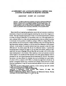
Accurate and Efficient Layout-to-Circuit Extraction for High-Speed MOS and Bipolar/BiCMOS Integrated Circuits F. Beeftink, A. J. van Genderen and N. P. van der Meijs Delft University of Technology, Faculty of Electrical Engineering P.O. Box 5031, 2600 GA Delft, The Netherlands email:
[email protected] Abstract In this paper, we describe how we have exploited the advantages of various methods for device recognition and modeling in a layout-to-circuit extractor, called Space. Hence, we have obtained a program that, for different technologies, can quickly translate a large layout into an equivalent network. The network includes layout parasitics of the interconnects and can directly be simulated by various simulation packages, such as Spice. The efficiency and accuracy of the extractor are confirmed by experimental results and enable a fast and reliable layout verification for both MOS and bipolar/BiCMOS technologies.
high-level design
circuit simulator
circuit network comparator
layout
Space
circuit + parasitics
fabrication
Figure 1: Space in a design flow.
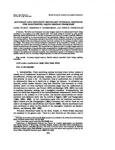
1 Introduction Today, layout verification for VLSI is a crucial part of IC design. For applicability, however, it must not only be fast and accurate, but it must also allow for various technologies. The layout-to-circuit extractor Space meets these constraints. It quickly translates a layout into an equivalent network that is an accurate model of that layout. Subsequently, circuit simulation and network comparison are convenient tools to accurately predict and verify the behavior of the design before fabrication, thus reducing design costs. This is summarized in the design flow of Figure 1. Modern (deep submicron) integrated circuits balance on the edge of IC technology in order to minimize delay times and increase data-throughput. As a result, the influence of layout parasitics can be crucial to the question whether or not the design meets the specifications. Hence, for layout verification based on circuit extraction, it is important to create (extract) accurate models for both the devices and the interconnects. Therefore, Space produces a network that not only contains active devices and their models, but also interconnect capacitances and resistances. With respect to other circuit extractors (e.g. [1–4]), the extractor described in this paper offers an unique combination of many techniques integrated into one single package. Figure 2 displays the flow diagram of our extraction methodology. The two stages identified by the solid boxes represent the actual extraction program and are briefly discussed
below. Using this two-step method, the extractor can easily be adapted to the simulation package that the designer will use: only in the last step the device models are generated. It also allows for an easy integration of the extractor in many different CAD-systems. The first extraction stage mainly consists of the recognition of devices and the extraction of relevant geometrical information, such as device areas and perimeters. In this stage, we distinguish between MOS and bipolar devices. Compared to MOS devices, it is not only harder to identify bipolar devices, but also to create appropriate simulation models for them. Therefore, for bipolar devices, we distinguish between the intrinsic (or active) part and the extrinsic part. The recognition of the intrinsic part requires some extensions to the techniques that are used for the recognition of MOS devices. The extrinsic device part, however, is modeled in a way that is similar to the interconnect parasitics, e.g. by series resistances and junction capacitances. The main device recognition algorithm that is used in the first extraction stage uses a hash-table to identify the circuit elements that are present and is described in Section 2. Subsequently, the extensions to this algorithm that are necessary for the extraction of the intrinsic bipolar devices are discussed in Section 3. The methods for extracting interconnect parasitics and the extrinsic device parts are also applied in the first stage and are briefly discussed in Section 4. Thus, the output of this stage is a circuit netlist that models the layout, including the (extrinsic) parasitic elements and the active devices with detailed geometrical data.
PROCESS
LAYOUT EXTRACTION
PRE-PROCESSING
Create hash-table
hash-table
unity parameters
IC
IC
n+
- Recognize (intrinsic) devices - Calculate device geometries - Model extrinsic devices - Create models for interconnect - Netlist (including parasistcs) - Device geometries
Derive unity parameters
IC
p base
p+ base
n+ n-epilayer
burried-layer
(a)
Create device models
CIRCUIT
Figure 2: Extraction flow-diagram.
The second extraction stage produces the device models by combining the geometrical information of the first stage and the process data. The devices are assigned to either predefined models that have fixed (measured) parameters or to models for which the parameters are evaluated using the geometrical device data. It is briefly discussed in Section 5. Hence, the final output of the extractor is a circuit netlist including the device models. It can directly be used as input for various simulation packages, because, in the second stage, the format is adjusted to the simulation package the designer prefers. Both performance and simulation results are presented in Section 6, confirming the efficiency and accuracy respectively. We conclude in Section 7.
2 Main Extraction Algorithm In this section, the basics of the main extraction algorithm are described. The extractor exploits a scanline algorithm and a corner stitching data structuring technique [2]. The advantages of this combination are described in [5]. The layout is investigated in a band around a so called scanline (a straight vertical line across the layout), that scans the layout from left to right. In this way, only a small part of the layout is processed at one time. During the scan-operation, an internal data structure is constantly updated. The data structure represents the devices that have been recognized, their geometries and their connectivity to the rest of the circuit. Using a corner stitching data structure has the advantage that information that is close to each other on the layout is also stored logically close together in the data structure. Furthermore, it enables various operations to efficiently search for and enumerate neighboring features in a layout. The corner stitching data structure represents the layout in terms of presence or absence of mask layers according to the paint paradigm [2]. Therefore, the layout is partitioned into a set of non-overlapping rectangles, called tiles. Each tile is assigned a specific color that denotes the masks present in the tile.
(b) Figure 3: a) Cross-section of a vertical bipolar transistor and b) its tile partitioning (top-view).
Figure 3 shows an example layout and its tile representation. For the device recognition, Space uses a hash-table that is keyed by the color of one tile or the combination of the colors of two neighboring tiles. This color is defined as a bit-vector with each bit representing a specific mask. For the masks that are present in a tile, the corresponding bits are set and all other bits are cleared. For each key (color), the hash-table contains a list that describes which elements are present in the tile. The basic element parameters such as sheet resistances and area capacitances are also included in this list. Each mask that is present in a tile is represented in the data structure by a so called subnode. During extraction, when the scanline proceeds, the electrically connected subnodes are merged into larger aggregates and represent the nodes (nets) of the circuit. If an element is characterized by an unique combination of mask-layers that are stacked on top of each other, it can be recognized by the color of a tile. When an element has been recognized, its terminals are connected to the appropriate subnodes of that tile and, consequently, to the nodes of the circuit. In this way, the connectivity between the elements is maintained and easily kept up to date.
3 Subgraph Isomorphism From the previous section, it may be concluded that the element recognition by the color of the tile is an efficient technique for recognizing most MOS and intrinsic vertical bipolar devices. Unfortunately, the intrinsic lateral bipolar devices cannot be described in terms of a unique combination of mask-layers stacked on top of each other. Therefore, for the recognition of these devices, we exploit another recognition technique that is based on subgraph isomorphism as explained below. In general, (bipolar) devices are characterized by the topology of certain junctions, that is the relative position of the junctions to each other. In the layout, lateral junctions are encoun-
n diffusion p’ isolation p diffusion
(a)
(b) Figure 4: a) Example layout consisting of three lateral devices and b) its polar graph representation.
tered on the edges of adjacent semiconductor regions of different polarity. Hence, they can directly be identified by the color of a tile and its neighboring tiles using the hash-table. The polarity of the semiconductor regions depends on the carrier type of the region. In bipolar technologies, there are two different carrier types: electrons (’n’-type) and holes (’p’-type). In the data structure, the semiconductor regions are represented by polnodes (short for polar node) and are defined as geometrically connected subnodes of the same carrier type. For all purposes, we need not distinguish between lightly and heavily doped regions. For increased accuracy, however, this can be done if desired. For the recognition of lateral bipolar devices, it is useful to represent the layout by a polar graph G p (V; E ), where V represents the polnodes and E the junctions in the layout. Figure 4 shows such a graph for an example layout. The polar graph can be constructed during the scanning of the layout using the mask-information of the tiles as described in the previous section. During the construction of this graph, several conventional graph search algorithms can be used for device recognition. Especially for lateral device recognition, subgraph isomorphism techniques [6] are suitable. When we apply these techniques on the polar graph representation of the layout, a device is recognized if a subgraph of the total graph matches a device model graph. Each basic device has its own unique device model graph that is typically specified by the user. In Figure 4, three different lateral devices are recognized (the subgraphs that are encircled by the dashed lines). The remaining polnode represents an isolation region and is not a part of a device. The largest subgraph represents a lateral multi-emitter
transistor. Actually, it is built by several smaller subgraphs that all match a device model graph of a lateral ’single-emitter’ transistor. In general, subgraph isomorphism is not very efficient due to initialization problems of the search [7]: usually, there are no clues about where and when to begin the search. In our case, however, the problem remains fairly simple because of two reasons: (1) we only trigger a search if a junction is recognized that is possibly a part of a lateral bipolar device, and (2) we can keep the diameter, the longest single path, of the device model graphs relatively small with an average length of approximately two. When a lateral device is identified, we simply connect its terminals to the appropriate nodes that are linked to the polnodes of the corresponding subgraph of the device. If different terminals of the device are specified by identical mask-combinations, we distinguish between them by heuristic rules. For the emitter and collector of a lateral bipolar transistor, for instance, we assume that the collector has the larger area. Further, we proceed with the scanning of the layout as described in the previous section.
4 Parasitics Modeling Interconnect Capacitances As illustrated in Figure 5, the extraction of capacitances is subdivided into ground capacitances (Cpps and Ces ), vertical coupling capacitances (Cppt and Cet ), lateral coupling capacitances (Cl ), and junction capacitances (Cjb and Cjs ). Using the hash-table, the capacitances Cpps , Cppt and Cjb are recognized from the color of one tile, and the capacitances Ces , Cet and Cjs from the colors of two adjacent tiles. The recognition of Cl requires an additional neighborhood search (over a limited distance) through the corner stitching data structure. The values of the various capacitances are by default computed using an interpolation formula [8]. The parameters in this formula are: area, edge length and distance between two wires. The junction capacitances are always computed using such an interpolation formula. Optionally, the other capacitances can be computed using an accurate three-dimensional boundary-element method [9]. top plate Cppt
Cet Cl
bottom plate Cpps
neighbor plate
Ces diffusion substrate
Cjs
Cjb
Figure 5: Parasitic interconnect capacitances that can be extracted by Space.
a
b
(a) c a1 0.66
a2
(a)
6
2
12
0.5
6 12
16 0.80.8 22
(b)
3
Figure 6: Illustration of the method employed by Space for accurate resistance extraction. a
3
10 1.33 3 16
3 1.33
c1
b1
b2
6
6
(b) c2
6
6
b 9.17
a
a
R
b
b
38.2
36.2 7.32
4.01
(c)
c
Ca
Cb
Figure 7: Illustration of the problem with symmetric πmodels.
Interconnect Resistances Like interconnect capacitances, (parasitic) interconnect resistances often (co-)determine IC performance and functionality. For example, wire resistance can cause intolerable voltage drops due to steady-state current flow or can cause spikes due to switching currents. Most resistance extraction programs operate by partitioning the interconnect polygons into smaller pieces based on a heuristic prediction of current flow and then use another heuristic procedure to combine the resistance of the fragments into the total polygon resistance [3]. However, the accuracy of these heuristics is hard to predict and the algorithms can break down on unexpected inputs. As a solution, Space exploits a technique derived from finite-element theory, thereby achieving increased accuracy and robustness [4,10]. Figure 6 presents an example of a layout (a) and the associated finite-element mesh for the polysilicon mask (b). The final resistances are computed from the mesh in (b) via Gaussian elimination of all internal nodes [4, 10]. Using a new algorithm for ordering the elimination steps [11], this finite-element method achieves nearly linear time complexity.
Distributed RC Effects In order to verify a circuit for the combined influences of a distributed interconnect resistance and capacitance, lumped RC models are needed. Traditionally, resistances and capaci-
37.6
Figure 8: Construction of a weighted π-model.
tances are computed separately and combined into one model afterwards, using heuristics like dividing the capacitance into equal parts over the nodes of the lumped resistance model. The resulting symmetrical π-models are in many cases inaccurate. RC models with several (symmetric) π-sections are also constructed, but these are inefficient for simulation because they contain too many nodes. Figure 7 illustrates the problem, where due to the non-uniform resistivity and capacitivity of the interconnect a symmetric π-model would be inaccurate. Instead, most of the capacitance of the path between a and b should be attributed to node b. As a solution, we employ a strategy that results in so-called weighted π-models [10]. In a weighted π-model, the values of both capacitances are adjusted to take the asymmetry of the resistivity of the path modeled by the π-section into account. The sum of both capacitances remains equal to the total capacitance of the path. The weighted π-models are constructed by first creating a detailed RC-mesh that is subsequently simplified by eliminating internal nodes. In doing so, the accuracy is ensured by preserving the first-order time constants (or Elmore delay times [12]) between the endpoints of the interconnect. This guarantees that the transfer function of the resulting network closely matches that of the detailed RC mesh and, consequently, that of the distributed RC interconnect. The process of constructing a weighted π-model is illustrated in Figure 8. In (a) a T-shaped interconnection is shown. In (b) an intermediate network is shown that models the distributed RC effects in detail. In (c) the final weighted π-network is shown.
Voltage [V]
6
4
2
Simulation input Simplified model output Detailed model output
0 0
1e-10
2e-10
3e-10
4e-10
evaluated for each different device geometry. Most device parameters, such as saturation currents and current gains, depend linearly on the device area and perimeter [14,15]. Other parameters, such as the non-linear base resistance in bipolar transistor models, are more difficult to determine, but can be approximated by fitting rules that are derived from measurements. Thus, the output of the second stage is a complete netlist that contains the devices and parasitics and includes the device models. It is also adjusted to the input format required by the simulation package that the designer prefers.
Time [sec]
In Figure 9, simulation results of the simplified model (solid curve), are compared to simulation results of the detailed model (dotted curve) for the T-interconnection of Figure 8. The voltage of node c is plotted for a ramp input voltage applied to node a.
Substrate Resistances Because the parasitic coupling between components via the substrate becomes more and more important, an accurate boundary-element method is implemented in Space for extraction of substrate resistances [9, 13].
5 Device Models In order to simulate the extracted network, (compact) models have to be constructed for the active devices that have been recognized in the first extraction stage. For simulators such as Spice, the input consists of a list of device instances with a reference to a device model or type. Thus, each device instance must be assigned a model specific for its geometry. In practical situations, when e.g. only standard devices have been used, good compact device models are already available or, when e.g. the process has been well-characterized, they can be easily constructed from the geometrical device parameters that have been obtained during the first extraction stage. In this case, it is allowed to use the method that is briefly described here. When entering the second extraction stage, the location, dimensions and connections of every device in the netlist are known. During this stage, the extractor selects for each device an appropriate predefined model that is specific for its geometry. Identical devices are assigned the same model. Basically, there are two different model types: the scalable and the substitution models. For the scalable models, all device parameters are known for a specific device geometry. Those devices in the netlist that are within a certain (specified) range of that specific device geometry are scaled to that model. The scaling factor is proportional to the intrinsic device area (for vertical devices) or perimeter (for lateral devices). For the substitution models, the device parameters are specified as (user-defined) functions of the device geometry and are
6 Experimental Results The extraction methods as described in the previous sections have been implemented in the layout-to-circuit extractor Space. In this section, we present some experimental results using Space. Table 1 shows the benchmark data as obtained on an HP 9000/735 computer. The table illustrates the performance when using the different options for capacitance and resistance extraction: ’-’ means no extraction of interconnect capacitances or resistances, ’c’ means extraction of ground capacitances, ’C’ means extraction of ground and coupling capacitances, and ’r’ means extraction of poly and diffusion resistances. The number of transistors differs from approximately 100 for the ’attenuator’ to almost 65,000 for the ’cordic’. Analysis of this data reveals that the increases for both the CPU times and memory, caused by the various (combinations of) methods to extract interconnect parasitics, is almost a constant factor that is independent of the size of the design. The relatively larger differences for the ’cordic’ are caused by the long power lines. These lines are modeled by many different circuit elements that have a capacitive coupling to other elements. They have to be kept in core in order to create accurate lumped RC models. The extracted ’attenuator’ circuit has been simulated using Spice and the results are displayed in Figure 10. The design is a controllable current attenuator for completely integrable hearing aids and is described in detail in [16]. In the figure, the 0
-20
Gain [dB]
Figure 9: Transient simulation of RC interconnect.
-40 Measurement Simulation -60 1e+02
1e+03
1e+04
1e+05
1e+06
Frequency [Hz]
Figure 10: Simulation and measurement results of the attenuator for different control currents.
Table 1: CPU time (in minutes:seconds) and memory usage (in megabytes) for different layouts and various (combinations of) interconnect extraction methods on a HP 9000/735 computer.
circuit attenuator detector logic array cordic
# tors 98 1,083 6,360 63,416
time 0.6 1.5 16.4 3:38.7
c mem. 0.359 0.372 0.787 2.800
time 0.8 1.7 19.1 4:11.7
C mem. 0.363 0.406 0.882 2.910
time 0.8 2.0 23.0 4:30.9
rc mem. 0.410 0.582 3.000 17.000
time 2.6 9.9 2:22.0 25:47.5
mem. 1.410 1.020 2.670 18.100
rC time mem. 3.2 1.590 12.7 1.830 3:10.5 13.800 35:19.3 82.000
simulation results for different control currents are given by the solid lines. Some measurements for identical control currents are given by the dashed lines and show good similarity.
[4] T. Mitsuhashi and K. Yoshida, “A resistance calculation algorithm and its application to circuit extraction,” IEEE Trans. on CAD, vol. 6, pp. 337–245, Jul. 1987.
7 Conclusion
[5] N. P. van der Meijs and A. J. van Genderen, “Space-efficient extraction algorithms,” in Proc. IEEE 3rd European Design Automation Conference, pp. 520–524, Mar. 1992.
In this paper, we presented a layout-to-circuit extractor for both MOS and bipolar/BiCMOS technologies. The program exploits the advantages of several recognition techniques, such as hashing and subgraph isomorphism. They are coupled to an efficient scanline algorithm and together enable a fast layout extraction for large VLSI designs. The extracted network is an accurate model of the layout and can also contain interconnect parasitics. The devices of this network are assigned to simulation models specific for the device geometry. This is performed in a separate stage of the extraction process and can therefore easily be adapted to the simulation package that the designer prefers. In the paper, both performance and simulation results have been presented. They illustrate the efficiency and accuracy of the implementation of layout-to-circuit extraction in Space. We have shown a completely automatic way of converting an IC layout, including full-custom bipolar devices, into a suitable input for various simulation packages. In combination with simulation or network comparison tools, the presented two-step extraction method enables accurate prediction and verification of both MOS and bipolar/BiCMOS designs and allows for an easy integration in many different CAD-systems.
Acknowledgements This research is sponsored in part by the Dutch Technology Foundation (STW) under grant nr. DEL 22.2810.
References [1] T. B. Hook, “Automatic extraction of circuit models from layout artwork for a BiCMOS technology,” IEEE Trans. on CAD, vol. 11, pp. 732–738, Jun. 1992. [2] W. S. Scott and J. K. Ousterhout, “Magic’s circuit extractor,” in Proc. IEEE 22nd Design Automation Conference, pp. 286– 292, 1985. [3] M. Horowitz and R. W. Dutton, “Resistance extraction from mask layout data,” IEEE Trans. on CAD, vol. 2, pp. 145–150, Jul. 1983.
[6] A. D. Brown and P. R. Thomas, “Goal-oriented subgraph isomorphism technique for IC device recognition,” IEE Proceedings, vol. 135, pp. 141–150, Dec. 1988. [7] A. P. Kostelijk, Verification of Electronic Designs by Reconstruction of the Hierarchy, PhD. thesis, Eindhoven University of Technology, Eindhoven, the Netherlands, 1994. [8] N. P. Meijs and J. T. Fokkema, “VLSI circuit reconstruction from mask topology,” INTEGRATION, the VLSI Journal, vol. 2, pp. 85–119, Mar. 1984. [9] T. Smedes, N. P. v. d. Meijs, and A. J. v. Genderen, “Boundary element methods for 3D capacitance and subtrate resistance calculations in inhomogeneous media in a VLSI layout verification package,” Advances in Software Engineering, vol. 20, pp. 19–27, Jan. 1994. [10] A. J. van Genderen and N. P. van der Meijs, “Reduced RC models for IC interconnections with coupling capacitances,” in Proc. IEEE 3rd European Design Automation Conference, pp. 132–136, Mar. 1992. [11] N. P. van der Meijs and A. J. van Genderen, “Delayed frontal solution for finite-element based resistance extraction,” in Proc. IEEE 32nd Design Automation Conference, pp. 273– 278, Jun. 1995. [12] W. C. Elmore, “The transient response of damped linear networks with particular regard to wideband amplifiers,” Journal of Applied Physics, vol. 19, pp. 55–63, Jan. 1948. [13] T. Smedes et al., “Extraction of circuit models for substrate cross-talk,” accepted for publication in Proc. IEEE/ACM International Conference on CAD, Nov. 1995. [14] H. F. F. Jos, “Bipolar transistor: Two-dimensional effects on current gain and base transit time,” Solid-State Electronics, vol. 31, no. 12, pp. 1715–1724, 1988. [15] H. C. d. Graaff and F. M. Klaassen, Compact Transistor Modelling for Circuit Design. Computational Microelectronics, Springer-Verlag, 1990. [16] A. v. Staveren and A. H. M. v. Roermund, “Low-voltage lowpower controlled attenuator for hearing aids,” Electronics Letters, vol. 29, pp. 1355–1356, Jul. 1993.