are used in signal processing applications [3]. The simple structure of these shift register based circuits enable accurate prediction of clock gating power savings.
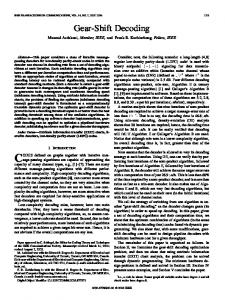
2010 IEEE 26-th Convention of Electrical and Electronics Engineers in Israel
Adaptive Clock Gating for Shift Register Based Circuits Israel Koren ECE Dept. University of Massachuset1s Amherst, MA 01003, USA
Shmuel Wimer Eng. School Bar-Han University Ramat-Gan 52900, Israel
beyond what is done for individual flip-flops requires more effort. It is therefore beneficial to study digital circuits whose state sequence can be derived directly from their structure. Shift register based circuits have this property and they include, for example, counters, Linear Feedback Shift Registers (LFSRs) that are used for pseudo-random number generation, serial adders, and Tapped Delay Lines (TDL) that are used in signal processing applications [3]. The simple structure of these shift register based circuits enable accurate prediction of clock gating power savings.
Abstract - Clock gating is a widely used technique for dynamic power reduction in VLSI design. In its most straightforward application it allows disabling the clock signal of a flip-flop once its state is no longer subject to changes. further
This paper and
extends
proposes
a
this
technique one
systematic
way
to
Itamar Cohen Eng. School Bar-Han University Ramat-Gan 52900, Israel
step
achieve
additional dynamic power savings based on the correlation of flip-flops' activities. Circuits based on shift registers are widely used in digital systems and we selected them to demonstrate the effectiveness of the proposed method. The
II.
best, worst and average cases for dynamic power savings
I.
CLOCK GATING OF FLIP-FLOPS
Fig. 1 shows how a sequential element can find out that its clock can be disabled in the next cycle. A XOR gate compares its output at the present cycle with the present data input, that is supposed to appear at the output in the next cycle. The elk_enable output of the XOR indicates whether or not a clock signal will be required in next cycle. The clock driver shown in Fig. lea) is then replaced by a 2-way AND gate where the clock signal is enabled. We will use the symbol in Fig. 1 (b) to represent sequential elements that incorporate generation of
tare analyzed.
INTRODUCTION
Market demand for low power mobile computing and consumer electronics products has refocused VLSI design in the last decade on lowering power and increasing energy efficiency. The clock signal of a digital systems is a major dynamic power consumer; typically responsible for 50% of the total dynamic power consumed. Many design methodologies and techniques to reduce the dynamic power have been developed, of which clock gating is the most popular and well established in the design community. Clock gating is employed in all levels: system architecture, block design [1], logic design and local circuits [2]. Clock enabling signals are usually introduced by designers at the system and block design phases, where the interdependencies of the various functions are well understood. Going down to the circuit implementation, it is very difficult to define such signals since the interdependencies of the state of various flip flops depend on the gate-level implementation which is usually automatically synthesized.
elk enable. Controlling the clock in each flip-flop by a dedicated gater using the flip-flop's elk_enable signal was studied in [4]. An implementation for LFSR has been discussed recently in [5], where after taking into account the power consumed by the extra circuitry, 10% net power reduction was reported. Additional power reduction can be achieved by reducing the number of clock gaters. We could control several flip-flops with a common gater if we knew that they are toggling simultaneously most of the time, thus achieving almost the same power reduction, but with fewer gaters. The grouping may contain up to several dozens of flip-flops in a single group, and is usually done in the physical VLSI design phase by clock tree synthesizers [6]. Such tools are focusing on skew, power and area minimization, and are not aware of the toggling correlations of the underlying flip-flops.
This paper presents an approach to maximize the clock gating at the circuit level, where the clock signal that is driving a given flip-flop is disabled (gated) once the flip-flop's state is not subject to a change in the next clock cycle. Clock gating does not come for free. Extra circuits are required for its implementation, and therefore, its potential benefit should be predicted beforehand. The data sequences, and hence the implied state transitions of flip-flops in digital systems like microprocessors, controllers, DSP and other applications, depend on the typical data processed by those. Assessing the effectiveness of clock gating may require therefore, extensive simulations, trace derivation and statistical analysis of sequential elements activity. As shown later in this paper, analyzing this data for further exploitation of clock gating 978-1-4244-8682-3/10/$26.00 ©2010 IEEE
Figs. 2 and 3 demonstrate the trade-off between the number of disabled clock pulses and the amount of hardware needed for the gaters' implementation. Fig. 2 shows how to join k elk_enable signals generated by distinct flip-flops into one gating signal. It saves the individual clock gaters used for every flip-flop in the expense of introducing an OR gate and a latch required to captures the enable signal and holds it until the next clock cycle. Clearly, the hardware save increases
000374
formulation of flip-flop grouping problem supplemented with optimal algorithm is presented later.
with k , but the amount of disabled clock pulses is decreasing. It is therefore required for gating scheme proposed in Fig. 2 to be highly beneficial that the clock enabling signals of the grouped flip-flops to be highly correlated. This paper develops later a technique for obtaining the flip-flops groups yielding maximal activity correlation. A simple example is shown in Fig. 3(a) where each clock cycle produces the appropriate value of elk_enable for a period of 10 cycles. Clocking each flip-flop separately, 14 clock pulses are disabled out of the total 20, yielding 70% savings in the cost of two AND gaters. Fig. 3(b) generates a joint gated clock with the aid of the gater in Fig. 2. As shown, while a single gater is used, the clock toggling power saving reduced to 60%. Obviously, a key factor in obtaining effective joint clock gating is in finding large groups of flip-flops having similar toggling. Accurate
Joining enabling signals of individual flip-flops suits very well clock-tree distribution network commonly used in digital circuits. A typical topological structure of such a tree is shown in Fig. 4. The clock signal enters the block at a pin called root, and then it is driven downstream to sequential circuits trough chains of drivers connected in a tree topology. It is possible to replace the drivers of the tree in Fig. 5 by k -way gaters proposed in Fig.2. A gater of the tree receives the enabling signals of its k children and then delivers the clock signal downstream accordingly. disabled, while in the worst case only
LFSR CLOCK GATING LFSR (Linear Feedback Shift Register) is a well-known circuit for pseudo-random number generation. Since the register flip-flops are toggling in a pseudo-random manner, it is interesting to investigate the potential power savings that can be achieved by disabling clock pulses to the flip-flops comprising the register, \vhen those clock pulses are unnecessary. Its analysis can serve other shift register based circuits whose toggling is known a priori (e.g., counters) or statistically (e.g., serial adder). Due to the random nature of the flip-flops' toggling we would expect only very limited power savings. We show however, that for a maximum period III.
pulses is
Consider the "time derivative" matrix M' defined as follows: (1 . 1)
j :::; N shows the toggling of flip-flop cycle. 0:::;
Cj
flop
j during the entire
if m
. = 111
.
'.J . ,+l,J, 1:::; i :::;2N -1,
othern1se
i + 1 mod N. An entry
0:::; j :::; N -I .
m
�
=
IS
0 means that flip
j does not change from state i to state
N(2N -1) 2N _
1,
i+
hence it
clock pulses in the cycle is
N(2N -1)
and the disabling ratio approaches
I
with
increasing N. We next search for the maximum period LFSR that yields the smallest number of disabled clock pulses. We denote a pair of successive states of M by ( w w1+1 ) and the number of bits
in two 1s in M'. We conclude that out of the N (2N -1) total
I'
they have in common by
2N
a
( /w w )) . Therefore, a((w. w. ) ) \ 1+1 1+1 I'
I'
equals N minus the Hamming distance between the two states, and it is the number of clock pulses required for the
for which the clock pulse can be disabled. We next summarize the above observations.
OS,
transition from Wi to wi+!. To ease the search for the desired
Given an N -bit LFSR with a period of 2N -1 states, the maximal number of clock pulses that can be
Proposition
1
disabled out of the
-1
_
{o
need not be clocked for this state transition and the clock pulse driving that flip-flop can be disabled. In the following we find the maximum, minimum and expected number of disabled clock pulses.
of M,
entries of M' for the Gray code LFSR, there are N (2N -1)
=
followed by
Obviously, each row of M' must contain at least a single 1 as otherwise there would have been two successive identical states in a cycle, which is impossible. Among all maximum period LFSRs, there is one that follows a Gray code for which successive states differ only in one bit. For this LFSR, there is a single 1 in every row of 1\I' with one exception - the transition from W = 10·· . 00 back to W = 00· . ·01 , resulting 1 2M
;u
m
The row index in (1.1) is taken cyclically, i.e., row 1
x
j at state i. Therefore, colunm
The paper shows the circuit
1/2k.
implementation and discusses the timing implications and circuit overhead.
(2N -1) N matrix. An M, 1:::; i :::; 2N, 0:::; j:::; N -1 represents the output
Q the flip-flop
of the total, while in a k -fan-out clock-tree the
1/4
average number is
Let the LFSR contain N D-flip-flops and have a maximal period, thus visiting 2N -1 distinct states, i.e., all possible states except the 00... 0 state. Let us denote by Wi' 1:::; i :::; 2N -1 entry my of
clock pulses
Since clock disabling requires extra circuitry in the register and clock network, the paper explores grouping the flip-flops of the LFSR to be driven by common clock gaters in an attempt to reduce circuit overhead. We show that in a binary clock-tree (fan-out of 2) the average number of saved clock
Counting the number ofdisabled elock pulses
the cycle states, and tabulate those in a
(2N -1)
are disabled, where a is some constant. It is further shown that the average number of disabled clock pulses is (N/2)(2N -1), half way between the worst and best cases.
N -bit LFSR (that cycles through 2N -1 states), in the best case (N -1)(2N -1) out of the total N (2N -1) clock pulses can be A.
a
1:
LFSR we assume for the moment that the word 00· .. 0 is
000375
M can be obtained by the inductive construction described below.
included in M (we will drop it later). To fmd the worst cycle
L:�a((Wj,Wj+l))' where the sum is taken cyclically. A pair ( ) comprising of two complementary codes clearly satisfies a(( W"))=0 . we wish to minimize
I
W
,
"
For the basis of the induction consider
W
w'
Clearly,
,
Therefore, if there exists an M that includes 2N-1 such pairs, no clock pulse could be disabled during the 2N-1 state transitions and M will correspond to the worst cycle. The order of the complementary pairs in the worst cycle
S,
M, and SI are concatenated and then a Most Significant Bit (MSB) with value 0 is added to every odd indexed row and a MSB of value 1 to every even indexed row, yielding M 2= [(00 ,11),(01,10 )l
((
1+1/\ ) =0 is invariant of the construction. For even we have a( ( w. w.+ ))= [. 11 a
w w I'
consider procedure
M3'
a( (Wj,Wj+1 ))
for i even,
The matrix M2 is obtained
-
[ a( ( [ a( (
W'K" W2K'+1
W2K' . w,
))
+
))
+
a( (
a( \
w,K' w,
W2K, W2K'+1
))] . ))] -
The subtrahend in the above equation follows from the the transitions from
W2K-'
to
wl
m
MK-l and from W2K to w 2K-' +l in SK-l. Notice that in the
[( 000, I ll), ( 001,110 ) , ( 011,100 ) , ( 010 ,101Jl Due to the alternating MSBs a ( ( W ' lI' + )) does not change in the i i
state pairs of (1.2) one is either 00· ··0 or 11···1, while the other has alternating 0 and 1 bits. Taking the evenness of K into account, the net increase in bit agreement is:
1
upper half of M 3, obtained from M2. In the lower half
a((100,01O ))
,
disappearance of
M3 =
turns into
[ (1 0 ) ]
(1.2)
IS:
' a (( OO,lO ))
=
M K_l and SK_l is:
i
which based on the above construction
obtained from S 2
[(0,1 ) ]
additional bit agreements between successive states involving
I'
To illustrate the general rule il)r
=
The first and second states of MK are 00···0 and 11···1, respectively, and 2. The last two states of MK consist of alternating bits; one has a Least Significant Bit (LSB) of 0 and the other a LSB of 1, or vise versa, depending on the evenness of K . We conclude that upon constructing MK, the number of
of an MSB in an alternating manner ensures that the pair ( w. w.HI ) , for i odd, consists of complementary states, hence
M,
1.
Notice that M2 includes all distinct 2-bit states. The addition
I'
=
as follows: 1. From M we generate a new matrix, denoted by 81, l where the states of every pair are swapped, thus,
(WI,W")
2.
a((O,I ))=a((I ,O))=O.
N 1 and
(1. 3)
in
0 Kodd. 2 K -2 K -1 = 2 Keven 2 2
l J l J{
M , which also preserves the number of identical bits. The 3 only increase in the count of bit agreements can occur at the two transitions between M2 (upper half of M ) and S2 (lower 3 half of In that case, there exists M3).
We denote by TN the total number of bit agreements resulting from repetitive application of matrix duplication. It then satisfies the following recursive equation: (1.4) TN �2TN_l +2,
procedure for M , state transitions between M and 83 satisfy 4 3 a((1101, 0111))= ( lOlO , OOOO =2· This bit agreement is
where a is some constant.
a ((110 , 011)) =a ((101, 000)) = 1· a(
whose solution is: (1.5)
Applying the construction
))
governed by the following two invariants of extending MK_1 into MK:
disabled out of
So far we have included the 00···0 state, but since LFSRs exclude it, we need to remove it iromM . This turns the 3N state sequence ···0101·.. , 00···0 and 11···1, into the 2-state sequence .. ·0101·. . and 11·..1, which adds IN12l bit
)
N
as follows:
clock pulses in the cycle is
O(2N)
and the disabling ratio approaches 0 with increasing N. Of most interest is the average case, for which the following can be stated. Proposition 3: Given an N -bit LFSR with a period of 2N -1 states, the expected number of disabled clock pulses in the cycle is (N/2)(2N -1 , half way between the worst and best
agreements between successive states, but does not change the complexity of T obtained in (1.5). We summarize the above
cases. The proposition follows by assuming that two successive states are random and independent of each other. The probability of a bit to change in a state transition is therefore
Given an N -bit LFSR with a period of 2N -1 states, the minimal number of clock pulses that can be
Proposition
N(2N -1)
2:
000376
0.5, yielding an average of
(N/2)(2N -1)
clock pulses that can
A gated clock tree can be constructed from joint gaters illustrated in Fig. 2. In practice, a joint gater will drive multiple flip-flops, but for the sake of analysis we will assume a binary tree. Fig. 5 illustrates how such gaters are connected to create the tree. Clearly, there is no point in enabling the clock buffer at the root. This follows from the LFSR very definition, where all states are distinct, so M' cannot contain a row whose bits are all 0, implying that the enabling signal at root is always 1.
be disabled. IV.
JOINT CLOCK GATING
As described above, gating the clock pulses of individual flip-flops requires an AND clock gater for each flip-flop, which constitutes a significant circuit overhead. Consider two flip-flops, whose toggling is highly correlated, namely, their outputs are likely to change simultaneously in the same states. In such a case, controlling the two flip-flops by a common clock gater is beneficial, even though we may end up sometimes clocking a flip-flop although it does not change its output while its counterpart does. If this happens only rarely, designing a common clock gater is beneficial. Driving several flip-flops jointly by a single clock buffer is a common practice supported by most commercial clock tree synthesizers. M 0
0
1
0
0
1
0
1
1
0 0 0
0 1 1
1 1
0
0
1
1
1
1
1
1 1
1
0
1
0
1 1
0 0
0 1
1 1
0 0
0
0
0
0
0
0
1
1
0
0
1
0
o
0
0
1
1
1
1
0
=
flop will be clocked 2N-1 times unnecessarily. In contrast, the first two columns contain only two 1 s each, so fue clock disabling of the corresponding flip-flops is highly correlated, justifying sharing a common gater by the two MSBs. Though not very likely to occur in an LFSR, the following observation is useful for an N -bit Gray-code counter. Sharing gaters by MSBs is useful allowing the saving of hardware resources in return to a very limited unnecessary clocking of flip-flops. Sharing gaters by LSBs is not as useful, as it produces excessive unnecessary clocking of flip-flops. Generally, since the 1 s in the columns of M' are mutually exclusive (except the first row), any pairing of flip-flops to share a common clock gater doubles the number of flip-flop clock pulses compared to using individual clock gaters. Still, compared to the total N (2N -1) clock pulses required without gating, this
M'
0 0
To asses the benefits of adaptive gating in a binary clock tree, let us return to the best LFSR case for clock gating, i.e., the one that follows a Gray code encoding as discussed in proposition 1. For illustration the corresponding matrices M and M ' for N 4 are shown below.
1
0
0 0
0 1
o 1
0
0
0
0
0
0
1
0
0
0
1
0
0
0
1
0
0
1
0
0
0
0
0
0
0
0
0
0
0
0 1
1
0
0 0
0
0
0
0 1
0
1
1
1 1
1
1 1
1
increase is small. On the other hand, the number of clock gaters has been reduced from N to N/2. More generally,
1
using joint gaters with k elk_enable inputs will cut the number of gaters to r N/k l but will increase the number of
Except the first row which contains two 1 s (due to the exclusion of the zero state from the LFSR), each of the other rows contain a single 1. Half of those 1s belong to the LSB column. Therefore, sharing a common gater by the LSB flip flop and any other flip-flop is undesirable since the other flip In the worst case discussed in proposition 2, joint clock gating is not useful at all since most of the flip-flops are toggling most of the time. More interesting is the average case stated in proposition 3, for which the following result holds. Proposition 4: Given an N -bit LFSR with a period of
clock pulses to k (2N - 1) . both columns have 0 in a given row, which has a probability ofl/2 x 1/2
1/4 to occur .
•
Similarly to flip-flop pairing at the leaves of a binary clock tree, we can proceed upwards by pairing two gaters and driving those by an upper level gater, thus constructing the binary clock tree bottom-up. The connections of gaters in a binary clock tree moe shown in Fig. 5 and inlply very strict delay constraints, which moe not discussed in this paper. When
2N -1 states and N an even number, the expected number of jointly disabled clock pulses is (N/4) 2N , namely, for
( -1)
an arbitrary flip-flop pairing in ml LFSR such that every pair shares a common clock gater, one quarter of the entire clock pulses can be disabled. Proof The entries of M' represent the successive bit transitions of the entries in M. Those transitions can be any of 4 possible types (i.e.,
=
the underlying circuit occupies significant silicon area ( N may reach few tens o f thousands in a large block), only the leaves and one or two levels above should be considered for an adaptive clock gating.
0 � 0, 0 � 1, 1 � 0 , and
v.
APPLICATION TO OTHER CIRCUITS
The result of proposition 1 is applicable to Gray code counter a, which from power saving perspective is the best since the disabling ratio approaches 1 with increasing N. A different clock gating approach was proposed in [7]. It is
1 � 1), are independent and each of them has the same probability. Consequently, half of M' 's entries are 0 and half are 1. Consider two arbitrary columns of M'. The joint clock gater is disabled for the two corresponding flip-flops only if
000377
delay line (TDL) widely used in DSP. Assuming that the
based on developing the specific Boolean expression for every flip-flop, desCIibing sufficient toggling conditions based on all
digital signal filtered by the TDL is random with equal
other flip-flops. This method is robust and has the advantage
probability of 0 and 1, the same power saving as for the
of not requiling latching disab Ie signals. It looks however, that
LFSR's average case can be expected. This is also true for the
the amount of logic per flip-flop increases with
shift registers storing the addend and augend in a serial adder.
N which is
undesirable. Another shift register application is for tapped
elk en1 clk_en2
�. •
elk_enk
elk o
Lateh
IrD-
---t- --.l T
-
•
en--.ioint elk_gated
-
'------'
Q
en1 ·
(a)
en--.ioint
en2
(b)
· ·
(b)
(a)
enk
elk_gated
elk
Figm'e 1: Enabling ofthe clock signal.
Figm'e 2: Joining
k enabling signals generated by distinct
flip-flops into one gating signal.
111010101111101010111 GO% elk Idle
(b)
(a) o
o
111010101110101010111
111010101011101010111
70% elk Idle
70% elk Idle
70% elk Idle
70% elk idle
Figm'e 3: Example ofjoint gated clock.
�
ICVC
....---.. -
..
.. C
E '0
level 0
� 1+-":::""::'-=---
n =
2N
=
c ..
backward connection of enabling signal
-'< c
..
U
"
.. ;, u �
m "
m "
�
m "
�
1U
'0'
!
a
2al: leaves ---.� •••
Figm'e 5: Replacing the drivers of a clock tree by
Figure 4: Clock tree distribution.
The
k -way gaters.
k input ofthe internal OR gate are propagating
bottom-up.
REFERENCES
R.,
[1) Benini L., Bogliolo A and De Micheli G, "A survey on design techniques
[5) Aloisi W. and Mita
for system-level dynamic power management," IEEE Trans. on VLSI Systems,
registers," IEEE Trans. on Circuits and Systems-II, Vol. 55, No.5, June 2008,
Vol. 8, No.3, June 2000, pp. 299-316.
pp. 546-550.
"Gated-clock design of linear-feedback shift
[2) Hosny M. S. and Yuejian W, "Low power clocking strategies in deep
[6) "Low skew - low power CTS methodology in SOC Encounter for ARM
submicron technologies," IEEE Inti. Can! on Integrated Circuit Design and
processor
Technology, ICICDT 2008, pp. 143-146.
http ://www.cadence.com/cdnlive/librarylDocuments/2009IEMEAI
[3) Weste N. H. E. and Harris D., CMOS VLSI Design - a Circuit and System
DI10 DaveKinjal ARM FINAL.pdf
cores,"
X.,
Perspective, Addison- Wesley, 2005.
[7) WU Q., Pedram M. and Wu
[4) Lang T., Musoll E. and Cortadella J., "Individual flip-flops with gated
power design of sequential circuits," IEEE Trans. on Circuits and Systems-I,
clocks for low power datapaths," IEEE Trans. on Circuits and Systems-II,
Vol. 47, No. 103, March 2000, pp. 415-420.
Vol. 44, No. 6, June 1997, pp. 507-516.
000378
"Clock-gating and i ts application to low