An Edge-Endpoint-Based Configurable Hardware Architecture for VLSI CAD Layout Design Rule Checking Zhen Luo, Margaret Martonosi and Pranav Ashar Princeton University and NEC CCRL {zhenluo, mrm}@ee.princeton.edu,
[email protected]
Abstract Design rule checking (DRC) is an important step in VLSI design in which the widths and spacings of design features in a VLSI circuit layout are checked against the design rules of a particular fabrication process. In the past, some efforts to build hardware accelerators for DRC have been proposed, but these efforts were hobbled by the fact that it is often impractical to build a different rule-checking ASIC each time design rules or fabrication processes change. In this paper, we propose a configurable hardware approach to DRC. Because the rule-checking is built in configurable hardware, it can garner impressive speedups over software approaches, while retaining the flexibility needed to easily change the rule checker as rules or processes change. Our work proposes an edge-endpoints-based method for performing Manhattan geometry checking; this approach is particularly well-suited to the constraints of configurable hardware. Although design rules do change over time, their intrinsic similarity allows us to propose a general scalable architecture for DRC. We then demonstrate our approach by applying this architecture to a set of design rules for the MOSIS SCN4N_SUB process. The hardware required per rule is quite small; we have implemented several design rule checks within a single Xilinx XC4013 FPGA. Our hardware, implemented on a Pamette board, runs at a clock rate of 33MHz. We also compare the performance of our approach to software methods and demonstrate overall speedups in excess of 25X.
1. Introduction Over the past several decades, integrated circuit die sizes have increased dramatically and simultaneously the smallest possible features on these dies have become much smaller as well. As a result, Design Rule Checking (DRC), which checks a VLSI layout's features for compliance with width and spacing rules, has become more and more time-consuming and compute-intensive. In the past, several approaches for hardware DRC accelerators have been proposed [1,3,5]. The main difficulty with prior, custom-hardware proposals has been their inflexibility. Fabrication processes evolve over time, with new layers or width/spacing rules being introduced. As such, design rule checkers implemented in hardware must be re-designed and rebuilt to address each
set of changes. Past hardware DRC approaches avoided this redesign cycle by accelerating only the basic primitives of DRC, not the specific rule checks. The drawback to such approaches is that they accelerate only a portion of the DRC and do not adequately address the true compute bottlenecks. Our proposal notes that while design rules do change over time and vary between fabrication lines, their fundamental form remains similar. Thus, our goal is to design a general-purpose skeleton for DRC that applies to nearly all fabrication design rules, and then also to tailor the rule-checking hardware for a particular fabrication process. Tailoring the rule-checks to an individual process allows for much better speedups and takes advantage of the inherent flexibility of configurable hardware. At the same time, the reconfigurations are likely to be infrequent enough (every 6-12 months) that the FPGA reconfiguration times have essentially no impact on performance. This paper presents our configurable hardware accelerator for design rule checking. In order to take the best advantage of the special characteristics of FPGAs, we have also developed a new DRC methodology that we present here. This edge-endpoint-based approach reduces the storage and sorting requirements for processing the layout files compared to prior work. This makes the approach particularly amenable to FPGAs and also reduces the cost considerably. Our evaluations of the DRC architecture indicate that it offers speedups of 25X or more over software approaches. The remainder of the paper is structured as follows. Section 2 gives background on design rule checking and surveys prior work on its hardware acceleration. Section 3 then gives an overview of our edge-endpoints-based approach, while Section 4 focuses in more detail on the resulting hardware DRC architecture. In Section 5, we offer a case study on how to apply our architecture to a specific fabrication technology example: the MOSIS SCN4M_SUBM process. Based on this example, Section 6 presents synthesis results and performance evaluations. In Section 7, we present the hardware prototyping with
Pamette, Finally, Section 8 discusses the future work, and Section 8 presents our conclusions.
2. Design Rule Checking: Background and Related Work Design Rule Checking takes as input a low-level description of the mask layers and features required for a particular VLSI design. Such data is produced by the CAD tool on which the layout was created. The goal of DRC is to identify places in the VLSI design in which design rules, such as the spacing between two features or the width of a wire, have been violated. Specifying design rules in terms of a parameterized width factor, typically referred to as lambda, sometimes allows the same design rules to be used as the feature size of the process changes. In spite of this, design rules change frequently and many fabrication processes, particularly in the sub-micron domain, will have subtly different design rules. Section 5 discusses the MOSIS SCMOS design rules on which our current implementation is based. There are two major types of design rule checking methods [2,3]. Bitmap methods were widely used in early approaches. The layout is rasterized into a grid of square cells, with each mask layer represented by a separate bit in each cell. Bit maps are attractive because of the simplicity of some operations such as Boolean operations (AND of two masks, for example) and space/width checking. Many bit map approaches are based on Baker’s algorithm [2]. This algorithm uses a 3 × 3 window to do the checking when minimum width is 2 and a 4 × 4 window to do the checking when minimum width is 3. There are, however, disadvantages to bitmap approaches. The first one is that bitmap approach requires processing a large amount of data; this requires large amounts of memory bandwidth and high parallelism in order to produce results with acceptable performance. In [3], special hardware “expands” the layer data on-the-fly into bitmaps to shrink intermediate storage requirements; nonetheless, the total amount of data being processed remains the same. The second disadvantage is that in a design system where the grid spacing (i.e., the minimum feature spacing) is much smaller than the minimum feature size, we need a much larger window size to check for width or spacing errors. If this is the case, significant time will be spent comparing error templates with windows [4]. Edge-based approaches, on the other hand, use edges to represent regions in each mask layer. This helps to reduce the amount of data needed in general and is less dependent on the mask resolution. Kane and Sahni [5] proposed a one-dimensional systolic architecture for design rule checking for Manhattan structures, with only
horizontal and vertical features. The edge files are divided into horizontal edges and vertical edges and each set is processed independently. Horizontal edges are checked for vertical width errors and horizontal spacing errors; vertical edges are checked for horizontal width errors and vertical spacing errors. The main disadvantage of this approach is that it requires non-deterministic amounts of hardware. The length of the systolic array is roughly determined by the number of horizontal edges along a horizontal line and this number varies significantly among different parts of the whole design. Most of the edge-based approaches instead use variations on scanline algorithms [1][6]. The mask layer data are transformed into an edge file that contains all non-vertical edges in the mask. Each edge is described by a pair of points, (Xmin, Ymin) and (Xmax, Ymax) along with an Orientation field indicating if the edge borders the region from above or below. Additional layer information is needed when multiple layers are handled together. The edges are sorted in a canonical order, by non-decreasing order of slope within ymin and xmin, before processing. A vertical scanline sweeps horizontally across the whole mask and only stops at the X-coordinates of all the edge endpoints. Edges that intersect the current scanline are then processed. This approach requires less hardware than previously-discussed approaches.
3. An Edge-Endpoint-Based DRC Approach The method we propose is focused on DRC for Manhattan structures. DRC with non-Manhattan structures increases complexity considerably. Since wires can intersect at arbitrary angles, it requires multiplications and divisions (generally implemented in floating point) to calculate intersecting points. This reduces its applicability to configurable hardware. For this reason, we focus here on accelerating DRC for Manhattan structures; in designs containing non-Manhattan regions, we could separately run software DRC on these regions, while using configurable hardware for the strictly Manhattan regions. We use a variant of the scanline algorithm discussed in the previous section, rather than directly implementing the previously-described algorithm, for several reasons described below: a.
First, edge-based processing leads to a fairly wide datapath. For Manhattan structures, we need at least 3 coordinate fields (Xmin, Xmax and Y) for each edge: two X-coordinates for beginning and ending points and one Y-coordinate for the edge. If each coordinate takes 18 bits as we use now, we need at least 54 bits just to store these three coordinates. This imposes
counterclockwise and the scanline passes over it again. In reality, since we are focused on design rule checking before fabrication, no true scanning occurs, but rather the features of the mask are extracted in a particular order from the layout file generated by the CAD tool.
Current Scanline Figure 1: Example mask layer with scanline.
constraints on FPGA size and overall system cost and performance. b.
c.
Second, some design rules require the generation of intermediate (or “working”) layers that are Boolean transformations of true layers. When an intermediate layer is generated in an edge-based algorithm, its edge file is not in canonical order, since the edge with the smallest X-coordinate of its ending point leaves the pipeline first. Thus an intermediate sort is needed [1]. This adds complexity to the control and data flow in the hardware system and extra hardware cost for temporary storage. Our variant algorithm avoids the need for these costly intermediate sorts. Third, we know of no prior work that fully addresses the edge-reconciliation problem [7]. A general method to obtain computational parallelism in DRC is to cut each mask layer into pieces and process each piece individually. This is possible both in bit-map approaches and edge-based algorithms. Spurious width/spacing errors, however, could be generated by the DRC system because some regions are split into pieces. Sewing regions back together imposes nontrivial performance overhead (especially for edgebased approaches) when the mask is divided into many small pieces.
For the above reasons, we propose a new approach that is amenable to configurable hardware and capable of solving the problems in b) and c). Our approach assumes a “virtual” scanline that passes over the mask layers, checking relevant design rules as it goes. As the scanline passes over the mask, it takes note of features like edges and their endpoints. In order to check vertical spacings or widths, the scanline will be oriented vertically, as shown in Figure 1 and will scan horizontally across the mask. In order to check horizontal spacings or widths, the mask is rotated by 90 degrees
Our method uses an edge-endpoint-based representation. That is, we categorize all the edges in a mask layer into horizontal edges and vertical edges and their endpoints are processed separately. By doing this, we can solve the problems mentioned above. From this point on, we will only talk about how to process the endpoints associated with horizontal edges. Endpoints associated with vertical edges will be processed in exactly the same way after the mask is rotated. 3.1 Representation An endpoint is represented in the following format: Y-coordinate
Layer O D P X-extension
Figure 2 Endpoint Format.
The Y-coordinate field represents the Y-coordinate of the edge endpoint. The Layer field indicates the layer this endpoint belongs to. The O bit indicates the orientation of the edge with which the endpoint is associated. O = ‘0’ if the edge is a forward edge, i.e. the edge borders the region from above; O = ‘1’ if the edge is a backward edge, i.e. the edge borders the region from below. The D bit indicates the direction of the current endpoint. D = ‘0’ if the endpoint is the starting endpoint of the associated edge. D = ‘1’ if the endpoint is the ending endpoint of the associated edge. The P bit indicates if the endpoint has been processed before. For the endpoints generated from mask layer data, P = ‘0’ and X-extension = 0. We will further discuss the P bit and X-extension fields later in this section. We maintain the endpoints in a canonical order. All the endpoints are sorted in increasing order by X-coordinate, Y-coordinate, layer and orientation. Two endpoints in the initial edge file “cancel” if they only differ in the D bit. That is, after endpoints are sorted, they are divided into groups with the same X-coordinate. Within each group they are sorted in increasing order by their first three fields. Note in the endpoint representation, there is no Xcoordinate information. Instead, a special endpoint of layer 0 is inserted before each endpoint group of the same X-coordinate and it records the X-coordinate value in its Y-coordinate field. 3.2 Scanline Maintenance
I/O Bus PCI Interface
0C0 1 1
DMA FIFO
C
2
Buffer 0,1
1
2 1
Merge
A 0 0 B
A B
Checking Figure 4 Selecting True Points. Memory for Intermediate Layer
Error Memory
Figure 3 Basic Processing Unit.
When the scanline is at a particular x coordinate Xc, we categorize and sort pending edges as follows: 1) Xmin = Xc, i.e., the edge starts from this scanline. 2) Xmax = Xc, i.e., the edge ends at this scanline. 3) Xmin < Xc < Xmax, i.e. the edge intersects this scanline. Endpoints from the first two categories are called new endpoints with P = ‘0’ since they have never been processed before. The points of the third category, however, are “inherited” from the previous scanline. Each time a category-1 edge startpoint is processed, it is passed along to the next scanline. This point inherits all the information from the starting endpoint except that now P = ‘1’ since they have been processed before. We refer to these points as old points. Old points are removed from the scanline when they meet the ending endpoints (category 2) of the edge. 3.3 Scanline Processing Endpoints of the current scanline, after being mergesorted with old points inherited from the previous scanline, stream into the processing unit as shown in Figure 3. Generally speaking, there are several processing steps, as described below. 3.3.1
Selecting True Points
In the input data from the CAD tool, there can be overlapped and coincident regions in some layers. These regions should be logically ORed to get the final region profile (see Figure 4). A point, whether it is an old point or a starting/ending endpoint of an edge, is called a true point, following Lauther’s terminology [11], if it is on the boundary of the final region. A true point is called a true endpoint, if it is one of the endpoints of the final region. Thus we need to select out the true points and only consider them in the design rule checking.
To help select the true points, we keep two counters for each layer: LC and RC. When a point enters the processing unit, the counters corresponding to its layer are updated in the following way: if (input point is a forward point) switch (input point) case “old point”: LC ++ ; RC ++ ; break; case “starting endpoint”: RC ++ ; break; case “ending endpoint”: LC ++ ; break; else /* input point is a backward point */ switch (input point) case “old point”: LC −− ; RC −− ; break; case “starting endpoint”: RC −− ; break; case “ending endpoint”: LC −− ; break;
Figure 4 illustrates the counter update process. Point C is a forward old point, thus both LC and RC are incremented. Point A is a backward starting endpoint, thus RC is decremented. Point B is a backward ending endpoint, thus LC is decremented. LC indicates if the area on the left side and below the current position is inside or outside the final region. If LC > 0, the left side below the current position is inside the final region; if LC = 0, the left side below the current position is outside the final region. LC should never be less than zero, however, unless there is an error in the endpoint file. RC similarly indicates the situation on the right side of the current position. In Figure 4, we can see that both the left side and right side below point C is inside the region, since LC > 0 and RC > 0. At Point A, the left side below it is inside the region and the right side below it is outside the region, since LC > 0 and RC = 0. Both the left side and right side of point C is outside the region, as indicated by LC = 0 and RC = 0. Special care has to be taken when dealing with coincident points. In considering two coincident points, the forward point of the two should always be sent to the processing unit; this lets us know that these two regions “overlap”. In our approach, this ordering is guaranteed by the canonical order of the endpoints.
Y-coordinate DIFFN = Y − YN DIFFP = Y − YP
N width, spacing P width, spacing N&P spacing
Layer YN
Layer Matching
YP O ON OP
O
D
Counter Update
YN & ON Updated if Y⊆ YP N&&OYP is true. Updated if Y⊆ P & Y is true.
Figure 5 Checking Unit for N and P Layers.
Thus a point is a true point if it changes the “inside the region” or “out of the region” status on either or both sides of the scanline. In Figure 4, A, B and C are the true points of the current scanline. A true point is a true endpoint if it changes the “inside the region” or “out of the region” status only on one side of the scanline. In Figure 4, A and B are true endpoints and C is not. 3.3.2
Checking Design Rules
Design rule checking boils down to different instances of width checking. Space checking of a specific mask layer, for example, is equivalent to width checking on the inverse of such a mask. Other types of checking, such as minimum overlap, can all be transformed to widthchecking in a similar way. This does not mean, however, that we have to transform the design to these intermediate forms before checking these rules. Instead, when multiple layers are present, all the rules that are associated with these layers can be checked simultaneously, as we will see in the example given later in this section. Design rule checking is also a local problem in that only “adjacent” regions interact with each other. In a bitmap approach, this locality is utilized by means of pattern matching on a two-dimension window. In an edge-based approach, this locality is utilized by processing only adjacent true edges along the scanline; this is also true in our edge-endpoint-based approach. Here adjacency not only refers to the adjacency within one layer, but among different layers as well. We define point and edge adjacency as follows: Definition Point A from layer I is said to be adjacent to a point B from layer J (I and J could be the same) if no other point from layer I or layer J is inside or on the boundary of the rectangle formed by these two points. Edge l and m are said to be adjacent if ∃ point A ∈ l and point B ∈ m, such that A and B are adjacent. Intuitively, consider two points A and B that are adjacent, and a third point C that is further from A than B is (and therefore not adjacent). Our definition of adjacency
allows us to recognize that design rule violations on these points can be recognized by comparing A and B only. Since C is further from A than B is, any design rule it violates with respect to A will also be violated by B. (Different adjacencies will be relevant for different layers and design rules.) Therefore, in our implementation, only the latest point of each layer along the scanline is stored in the Y-coordinate register of that layer for comparison with current true point. Once a true point from a layer is determined, the checker circuit for each design rule needs: (1) the Y-coordinate differences between this point and the latest points of each layer, and (2) the orientation of this point and the orientations of the latest points of each layer to find possible errors. Figure 5 shows a block diagram of a DRC system for N and P diffusion layers. Here, there are rules for minimum width of an N- diffusion, minimum width of a Pdiffusion, minimum spacing between two N-diffusions, minimum spacing between two P-diffusions and minimum spacing between an N-diffusion and a Pdiffusion. However, not all the rule checkers are activated when a true point from N or P layer is filtered out. For example, when a true point of N-diffusion layer is filtered out, the rule checker for minimum width of an Ndiffusion is activated only if the latest N point is forward (ON = 0) and the current N point is backward (O = 1). The rule checker for minimum spacing of an N diffusion is activated only if the latest N point is backward (ON = 1) and the current N point is forward (ON = 0). The rule checker on spacing between an N diffusion and a P diffusion is activated only if the latest P point is backward (OP = 1) and the current N point is forward (ON = 0). Similar activation criteria apply for all the other design rule checkers.
3.3.3
Handling Other Cases Using Virtual Edges
The design rule checking hardware described above is able to find all the design rule errors along a scanline. Thus if all the vertical and horizontal scanlines are processed, we should be able to find all the errors along any vertical or horizontal line. Our design would be complete now except for a special type of error, shown in Figure 6. In Figure 6, the central box has spacing errors with the surrounding four boxes. That is, if we expand the central box by the minimum space d, the expanded region (the dotted box in the center) will intersect all four boxes. However, this case escapes our DRC hardware thus far since no scanline will cross both the edges from the central box and the four boxes around it. Thus a natural
d B
A
d Q D
Figure 7 Mask Slicing.
C
3.3.4
Figure 6 Virtual Edges.
way to solve this problem in our existing hardware framework is to extend some edges of the central box or the boxes around it by d, so that scanline processing will be able to find the error. We call these extended edges virtual edges. Each point on a virtual edge is a virtual point. A virtual point inherits the Y-coordinate, Layer and Orientation information from the edge that generates it. Virtual points are old points, so P = ‘1’. We use the D bit to differentiate virtual points and normal points. If D = ‘0’, it is a virtual point; if D = ‘1’, it is a normal point. Unlike normal points that are automatically cancelled when they meet the ending endpoints, virtual points expire according to their X-extension bits. When the virtual point is first generated, the X-extension bits record the value of d. Assume the scanline moves to the right by d’ after the current scanline has been processed, then the X-extension bits of all the virtual edges are updated by subtracting d’ from themselves. If the value of the Xextension bits is less than or equal to zero, the corresponding virtual edge is cancelled. When multiple layers exist in the system, we set d to the value of the largest value of minimum width/spacing requirement concerning this layer. In order to minimize the number of virtual edges and to better accommodate virtual points in our method, we only generate virtual edges when: 1) The right side of a forward true ending endpoint is outside the region. This is used for space checking; OR 2) The right side of a backward true ending endpoint is inside the region. This is used for width checking. Thus in Figure 6, only B and D are generated as horizontal virtual edges, only A and C are generated as vertical virtual edges (Rotate the picture by 90 degree counterclockwise). Q will not be generated. Furthermore, we stipulate that a virtual edge never updates the Ycoordinate register of its layer.
Flagging Errors
To avoid flagging the same error many times, an error between current point and a latest point should only be flagged in the following two cases: 1) The current point is a true starting endpoint 2) The latest point is a starting endpoint and the current point is either a true point or a virtual point. The design rule checking system we describe above will find all the design rule errors between adjacent edges and will not generate repetitive errors. A proof of this claim can be found in [11]. 3.3.5
Generating Intermediate Layers
Sometimes intermediate layers are needed for further design rule checking. For example, a gate “layer” is usually involved in many design rules but is not explicitly a layer in the layout file. In such cases, special working layers are generated for checking several design rules. Such layers are often Boolean transformations on true design layers. Thus points can be selected using the techniques described in 3.3.1. Unlike traditional edgebased hardware systems, the intermediate layers generated here are in canonical order; thus they can be further processed while they are being generated. 3.4 Exploiting Parallelism Each mask layer can be sliced in vertical directions when dealing with horizontal edge endpoints (Figure 7) and in horizontal directions when dealing with vertical edge endpoints. Each slice can be individually processed. Since all virtual edges crossing the cut disappear from the slice on the right, we need to extend each slice a length d to ensure that these virtual edges are properly checked. Here d is the maximum length of all the virtual edges, which is equivalent to the largest minimum width/spacing required in all the design rules. We thus expect a performance penalty of d/s, where s is the width of each resulting slice. Edge reconciliation does not impose a big problem for our system since errors are only checked along the scanline direction. No spurious error will be generated by our system. Repetitive errors will be generated in the
overlapped region. They can be easily removed by “ORing” the errors collected from all slices.
4. Hardware Architecture Our hardware architecture is composed of one or more basic processing units (Figure 3). Each basic processing unit resembles the hardware architecture described in [1]. The Memory in Figure 3 gets the edge endpoints (i.e. new endpoints) from mask layers and the buffers store the “inherited” endpoints (i.e. old endpoints) from the previous scanline. Since the processing unit generates the old points for the next scanline while consuming the old points generated by the previous scanline, we keep two buffers. Buffer 0 is being read while buffer 1 is being written and vice versa. A Merge unit is used to maintain the scanline. Since both the data from the memory and from the buffer are in their canonical order, the merge unit does a simple two-way merge sort to generate the final data stream for processing. In addition, the merge sort unit also takes care of “retiring” old points and virtual points. As mentioned in Section 3.2, old points are removed when they meet the ending endpoints. Each old point has the same representation as the corresponding ending endpoint except for the P bit, which is the least significant bit in comparison; thus it will definitely meet the ending endpoint in the merge unit and it will be cancelled then. For virtual points, as mentioned in Section 3.3.3, the Xextension bits of the virtual points are updated in the merge unit, and virtual points are cancelled if X-extension bits are less than or equal to zero. The checking unit is different from each basic processing unit. Its basic structure is shown in Figure 5. For each layer, we need a set of counters and an additional subtractor. Thus the hardware cost grows almost linearly with the number of layers we send to each checking unit. The only exception is the number of design rules involved. If all layers processed by a checking unit interact with each other, the number of design rules is roughly quadratic to the number of layers. When an intermediate layer needs to be generated, the data from the checking unit will be fed into the memory of one or more subsequent basic processing units. Temporary storage is required to store this intermediate layer. The merge unit of the subsequent processing units should be able to get the data from its own memory and from this temporary storage and does a preliminary merge sort to keep the new endpoints in canonical order.
Rule 1 – Well Rule 2 – Active
N-well, N-high-voltage Active, N-well, N-high-voltage, N-plus-select, P-plus-select Rule 3 – Poly Poly, Active Rule 4 – Select N-plus-select, P-plus-select, gate, contact, active Rule 5 – Contact to Poly contact, Poly, gate Rule 6 – Contact to Active contact, gate Rule 7 – Metal 1 metal 1, contact Rule 8 – Via 1 via 1, metal 1, Poly, active Rule 9 – Metal 2 metal 2, via 1 Rule 14 – Via 2 via 2, via 1, metal 2 Rule 15 – Metal 3 metal 3, via 2 Rule 21 – Via 3 via 3, metal 3 Rule 22 – Metal 4 metal 4, via 3 Table 1 SCN4M Related Rules and Layers. Rule Description λ 1.1 Minimum Width of Well 12 1.2 Min Spacing for wells of different potential 18 1.3 Minimum Spacing for wells of same potential 0 or 6 2.1 Minimum Width of Active 3 2.2 Minimum Spacing between active 3 2.3 Source/Drain active to well edge 6 2.4 Substrate/well contact active to well edge 3 2.5 Min spacing between active of different implant 0 or 4 Table 2 SCMOS_SUBM Layout Rules – Well, Active. [10]
5. Design Rules Analysis Based on the hardware architecture described above, we have done a proof-of-concept implementation for the MOSIS submicron design rules [10]. In this section, we analyze the MOSIS submicron design rules and in the next section, we present our experiment results. 5.1 Introduction to SCMOS Design Rules For this work, we focused on the MOSIS SCMOS_SUBM design rules, used for sub-micron fabrication. There are 27 SCMOS layers possible overall, but for a specific fabrication process, only a subset of the above layers are used. We concentrate here on the SCN4M_SUBM process for digital circuits. This process is a 0.4µm N-well process with 4 metal layers. Table 1 lists the related design rules for this process and the layers they involve. Each rule in Table 1 is broken down into several concrete design rule checks. For example, Rule 1 and Rule 2 are listed in detail in Table 2. In all these rules, the largest minimum width/spacing in these rules is 18 λ. This will impact the time that edges and points spend recirculating through the design rule checker. The values of minimum width/spacing specified in the rules are all multiples of lambda except Rule 5.2 and Rule 6.2 where half lambda is used. This granularity impacts the total
Metal 4
Unit
Via 3
Merge Check
Xilinx part number XC4013e-2 XC4013e-2
CLB used 177 262
Flip- Pipeline Speed flops stages (MHz) 312 4 33 419 4 33
Metal 3
Table 3 Synthesis Results for Merge and Checking Unit. Via 2
For this reason, our hardware design allows at most 5 layers to be checked by a basic checking unit.
Metal 2 Via 1 Metal 1 Contact N+-select
Poly
P+-select
N-Well
Active
N-volt
Figure 8 Layer Interaction Graph.
number of points that need to be processed for a given die size.
Thus we divide the layers into several groups and process them independently. From Table 1, we derive the layer interaction graph shown in Figure 8. An edge is added if there is a design rule between these two layers. Our objective is to divide the graph into several cliques such that each clique has less than 5 layers and the duplicated layers are minimized. Here is how we divide the groups: Group 1: Poly, Active, N+-select, P+-select. Intermediate layers N-active and P-active are generated. Group 2: N-active, P-active, N-well, P-well Group 3: Poly, Active, Contact, Via1 Group 4: Contact, Metal1, Via1, Metal2, Via2 Group 5: Via2, Metal3, Via3, Metal4
5.2 Width Analysis We assume all the endpoints on the layout are on a 0.5λ × 0.5λ grid. Since λ = 0.2µm, the grid spacing is 0.1µm. If the maximum die width is 2cm, then we can have at most 2×10⁵ points on a vertical line. Thus we use 18 bits to store the X and Y-coordinates. Since there are 14 layers involved in the related design rules as shown in Table 1, 4 bits are used to store layer information. Since the largest minimum width/spacing is 18 λ and the grid is 0.5λ, the largest value for X-extension bits would be 36, so we use 6 bits to store it. From Figure 2, we need 31 bits for an edge endpoint. For simplicity, we use 32 bits for each endpoint and the one extra bit is given to the layer field since some intermediate layers might be generated on the fly. 5.1 Layer Analysis Theoretically speaking, we could have sorted all the edge endpoints from all mask layers and sent them through a large checking unit to figure out all the design rule errors. However, as mentioned in Section 4, the hardware requirement grows more than linearly with the number of layers involved. As shown in Figure 5, each incoming endpoint’s Y-coordinate is sent to a subtractor. If there are more than 14 subtractors in our hardware, routing will be a problem since the Y-coordinate is 18 bits wide. Even if the routing were possible, we would expect a large delay.
6. Experimental Results To test our ideas, we implemented a general merge unit as well as a check unit built specifically for Group 2. Since the merge unit is almost the same among different groups, we keep the merge unit and the checking unit on two separate FPGAs. 6.1 Synthesis results We used the Synopsys fpga_analyzer tool (1998.08) to generate .sxnf files from our VHDL input and we used Xilinx Foundation tools (V1.3) for the synthesis. We targeted our design at the speed of 33 MHz for the merge and check units and specified this information in the timing constraint file (.pcf file), where we listed this requirement for all the critical paths. After successful placement and routing, the synthesis results we get for the above design are listed in Table 3. Most notably, our design fits in a Xilinx 4013 part and achieves the targeted clock rate for both units. 6.2 Comparison against software To compare the hardware performance against software, we wrote a C program for our hardware implementation and tested it on several small CIF files (see Table 4). These CIF files were derived by synthesis and place-androute of benchmark examples in BLIF format using the Octtools tool suite from UC Berkeley. We wrote another
CIF files # of # of # of total scan input points lines points C17 25 229 863 C432 52 1340 7859 C499 37 1029 5506 C880 44 1144 6482 C1355 37 1029 5506 C1908 40 1228 7017 C2670 45 1517 8938 C3540 40 1360 7829 C5315 54 1518 8820 C6288 48 1296 7311
Cycle Ratio Ratio of # of softtotal pts/ ware cycles of software / by pixie hardware input pts 3.77 : 1 567327 657.39 5.86 : 1 4259747 542.02 5.35 : 1 3052718 554.43 5.67 : 1 3540159 546.15 5.35 : 1 3052718 554.43 5.79 : 1 3814853 543.66 5.89 : 1 4806229 537.73 5.76 : 1 4234389 540.86 5.81 : 1 4775876 541.48 5.64 : 1 3993868 546.28
Software runtime by pixie 2.71ms 22.12ms 15.53ms 18.24ms 15.53ms 19.68ms 24.93ms 21.85ms 24.72ms 20.55ms
Hardware Hardware Hardware runtime speedup speedup (150Mhz) (500Mhz) 0.0259ms 105 37.2 0.2358ms 93.8 28.1 0.1652ms 94.0 28.2 0.1945ms 93.8 28.1 0.1652ms 94.0 28.2 0.2105ms 93.5 28.0 0.2681ms 93.0 27.9 0.2349ms 93.0 27.9 0.2646ms 93.4 28.0 0.2193ms 93.7 28.1
Table 4 Experiment Results.
converter to convert the CIF files to our input format. Since the hardware we have implemented only performs design rule checking on N-well, N-high-voltage, N-active and P-active layers, we extracted from the CIF file the endpoints of these layers and sorted them in their canonical order. The resulting file is the input for both our software and hardware. To optimize the software performance, we used an integer for each of the fields in the endpoint. We also tried to replace as conditional jumps by Boolean operations wherever possible. We compiled our software on an SGI workstation running IRIX 6.3 IP32 system V with “cc – O3” where global optimizations and procedure inlining are performed by the compiler. Then we used pixie to instrument the code based on basic blocks and prof –pixie –invocations to collect the data on total number of points being processed and software cycles and execution time in Table 4. We ran the software on an SGI O2 workstation with a single 4-way superscalar MIPS R10000 processor running at 150MHz. Pixie uses the instruction scheduling model of this processor to obtain the data on software cycles and execution time. The cycles per instruction (CPI) obtained by pixie is 0.881, but since pixie is unable to perform instruction scheduling bigger than a basic block, we expect the true CPI to be higher. The last column in the table shows the projected speedup over the software run on a MIPS R10000 processor, if it were clocked at 500MHz rather than 150MHz. From this table we can see, by using the hardware acceleration, we expect to achieve an average hardware speedup of 93.6 times (excluding C17) over the software run on a 150MHz MIPS R10000 processor and an average hardware speed up of 28.0 times (excluding C17) over the software run on a 500MHz MIPS R10000 processor.
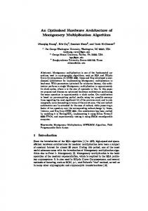
7. Hardware Prototyping on a Pamette
Download/ Readback
SRAM0 16
LCA0 (Merge) 36 PCI 64 PIF BUS
clock
36
20
40
LCA1 (Check)
LCA2 (FIFO)
36
LCA3 (Pass)
16
SRAM 1
Pamette board
Figure 9 DRC block diagram on a Pamette Board.
The implementation and performance results presented thus far represent VHDL designs and simulations. We have also mapped our design to the PCI Pamette board [12] for hardware prototyping. The Pamette hardware architecture is somewhat different from our ideal hardware architecture described in Section 4. Figure 9 depicts how the design originally shown in Figure 3 is mapped to the four XC4010e FPGAs (i.e. LCA0 - LCA3) of the Pamette. We put the merge unit on LCA0 and the check unit on LCA1. Instead of building two buffers for storing old points, we configure LCA2 to be a synchronous FIFO 256 entries deep. LCA3 is used to pass the old points generated from the Check unit (LCA1) to the FIFO (LCA2). We first configure the LCAs on the Pamette to download input endpoints into the SRAM0 on the board through the PIF, the PCI interface. Then we reconfigure the board to our design to process these input points. The Merge unit reads new endpoints from SRAM0 and old points from the FIFO and outputs the current scanline point stream to the Check unit. Check unit performs rule check on this point stream, sends design rule errors to SRAM1 and writes the old points to the FIFO through LCA3. When the whole process is complete, the board is reconfigured again to read the errors from SRAM1 to the host machine.
As shown in Figure 9, the bus width between LCA3 and LCA2 is only 20 bits wide. Among these 20 bits, only 16 bits can be used freely, the other 4 bits have some restrictions which make them hard to be utilized by our application. Since we need at least one bit for the “write_enable” signal on the FIFO, the representation for old points has to be less or equal than 15 bits wide. Based on data width analysis of the benchmarks shown in Table 4, we tailored our original point representation (see Figure 2) as follows. We use 7 bits for Y-coordinate, 2 bits for Layer, 1 bit each for Orientation and Direction and 4 bits for X-extensions. Since bit P is always ‘1’ for old points, we omit the bit P in this representation. Pamette board has three modes [12]: static mode, transaction mode and miscellaneous mode. In our runtime implementation, we used static mode throughout the process and we used clkusr [13] to provide a 33MHz clock for the four LCAs. The correctness of the board has been verified by running through our entire suite of test examples.
8. Future Work While the Pamette board is useful as a proof-of-concept, we ultimately intend to build a specialized FPGA board for design rule checking. This board will have sufficient data buffering to handle large designs, and can also include several FPGAs in order to check a number of design rules in parallel. This paper has focused on Manhattan structures in which all lines are either horizontal or vertical, and proposes that non-Manhattan structures be handled via software DRC. We are currently considering the hardware costs of handling special cases of non-Manhattan structures in hardware. For example, edges intersecting at 45-degree angles are the most commonly allowed non-Manhattan structure. The constrained geometry of these 45-degree angles greatly eases their intersection calculations. In such a process, all the geometric structures can be comprised of either quadrilaterals or isosceles triangles, and the spacing computations require no floating point calculations; spacings can be inferred from manipulations of known wire lengths.
9. Conclusions Because of the intrinsic similarity between different design rules [9], we have showed in this paper that hardware checking system for different design rules can be accommodated in a general scalable architecture. The variation between design rules of different fabrication processes makes configurable hardware an ideal candidate for the rule-checking unit in our general architecture. This
paper describes and validates an edge-endpoint-based geometry checking method for Manhattan structure, that is amenable to configurable hardware implementation. In comparison with previous edge-based methods, our technique uses a smaller datapath width, simplifies data flow control and easily handles the edge reconciliation problem. As a verification of this general architecture, we analyzed the design rules of SCN4M_SUBM process from MOSIS and implemented the essential hardware for checking a subset of the design rules. The final hardware system runs at 33 MHz and offers a speedup of more than 25X over the conventional software run on the state-of-the-art microprocessors. References [1] Eric C. Carlson and Rob A. Rutenbar, “A Scanline Data Structure Processor for VLSI Geometry Checking”, IEEE Trans. computer-aided design, vol CAD-6, NO. 5, Sep. 1987 [2] C.M. Baker, “Artwork Analysis Tools for Integrated Circuits”, MIT/LCS/TR-239, Master’s Thesis, MIT 1980 [3] L. Seiler, “A Hardware Assisted Design Rule Check Architecture”, Proc. 19th Design Automation Conf., June 1982, pp. 235-238 [4] Steven M. Rubin, “Computer Aids for VLSI Design”, 2nd edition, Addison-Wesley Publishing Company, 1994. [5] R. Kane and S. Sahni, “A Systolic Design Rule Checker”, Proc. 21st Design Automation Conf., Jun 1983, pp. 243-250 [6] T.G. Szymanski and C.J. Van Wyk, “Space Efficient Algorithms for VLSI Artwork Analysis”, Proc. 20th Design Automation Conf., June 1983, pp.734-739 [7] George E. Bier and Andrew R. Pleszkun, “An Algorithm for Design Rule Checking on a Multiprocessor”, Proc. 22nd Design Automation Conf., June 1985, pp. 299-304 [8] U. Lauther, “An O(N log N) algorithm for Boolean mask operations”, Proc. 18th Design Automation Conf., July 1981, pp. 555-562 [9] B.W. Lindsay and B.T. Preas, “Design Rule Checking and Analysis of IC Mask Designs”, Proc. 13th Design Automation Conf., June 1976, pp. 301-308 [10] MOSIS service, “MOSIS Scalable CMOS (SCMOS) Design Rules”, Revision 7.2, http://www.mosis.org/New/ Technical/Designrules/dr-scmos72.html [11] Zhen Luo, Margaret Martonosi, and Pranav Ashar, “A Configurable Hardware Design Rule Checker”, Princeton University Department of Electrical Engineering. Technical Report #CE-99-1. [12] Mark Shand, “PCI Pamette: Generic PCI Board”, http:// www.research.digital.com/SRC/pamette/ [13] Mark Shand, “PCI Pamette user-area interface for firmware V1.9”, http://www.research.digital.com/SRC/pamette/