This document is provided for informational purposes only. It cannot be published without written consent of Miller Freeman, Inc. Copyright (c) 1999 by Miller Freeman Inc., all rights reserved.
An FPGA Implementation of a Digital QRS Detector James A. Gilbert, Saint Vrain Technologies, LLC. David J. Farrell, Colorado Electronic Product Design, Inc. Email:
[email protected] ABSTRACT Advances in Field Programmable Gate Array (FPGA) density allow applications to be implemented in a single chip, which previously were reserved for Digital Signal Processors (DSPs), microcontrollers or Application Specific Integrated Circuits (ASICs) containing general purpose processor cores. This paper demonstrates the design of a heart rate monitor implemented on an FPGA with minimal external analog components and includes oversampling decimation filters, QRS detection and display output of R-R beat rate. 1. Introduction Cardiotachometers (heart rate monitors) are used in a variety of instruments from simple exercise monitors to subsystems of electrophysiologic (EP) stimulation and recording systems. At the core of all electrocardiogram (ECG) applications such as heart rate monitors is a method for the accurate detection of the QRS complex. Faster and more accurate QRS detection in portable devices has become possible with the proliferation of DSPs. The purpose of this work is to explore the possible use of Very High Speed Integrated Circuit Hardware Description Language (VHDL), available FPGA technology and minimal external analog components to implement a complete portable heart rate monitor. This FPGA based implementation is intended as a reference design to be used in place of a general purpose DSP or microcontroller and the glue logic typically required for I/O interface and memory.
2. Review of the Problem Small size, low cost and low power are all critical considerations for portable and implantable ECG devices. While analog QRS detectors can and have been designed to meet all of these criteria, they have been reported to be less robust and accurate in some applications when compared to a digital design. [1, 2] The low cost, power and size of general purpose microcontrollers in portable ECG applications has made them ubiquitous. The primary disadvantages of most general-purpose microcontroller cores are the serial nature of their execution of instructions (usually limited by the size of the CPU) and their limited math capabilities, not the least of which is their small bit width representations. Low-cost fixed-point DSP's, while suffering little or none of the mathematical performance limitations of the typical microcontroller, are generally more expensive and power hungry. Though some new cores have been introduced with ultralow power, low clock speed SingleInstruction-Multiple-Data (SIMD) computational architectures (most notably AudioLogic) for medical and other portable applications, generally, DSP cores are still serial in nature and therefore require relatively high clock speeds. For low power applications, the problems with the application of general-purpose cores are further exacerbated by the amount of internal data memory that consumes much of the power and space even though much of it typically goes unused. ASICs have been used in many portable medical applications with a great deal of success, but their development process can
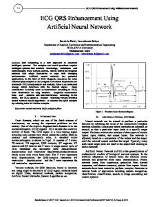
be lengthy when one is restricted only to computer simulation for verification. [2, 3, 4, 5] Using an FPGA during the development process can improve the verification procedure. The key advantages an in-circuit-programmable FPGA has as compared to most general-purpose cores are speed of computation, power efficiency (due primarily to the parallel processing of state inputs) and glue-less user configurable I/O. Among the disadvantages of an FPGA are its higher unit cost (system cost may differ considerably depending on the implementation, however) for comparable bit accuracy and the low level, i.e. gate level, at which the FPGA design must be accomplished. Using the FPGA as a prototype step towards an ASIC can reduce this unit cost and in most cases the power consumption, while advances in VHDL tools and available DSP library functions have eased design difficulty. 3. Functional Description of the System The design goal for this system was to create a general-purpose ECG processing platform based on an FPGA and a minimal amount of external components. This paper reports on the development of this hardware platform and the implementation of a simple QRS detector within its framework. The following summarizes the subsystems of the prototype: Analog Circuitry Instrumentation Amp Anti-aliasing filter ADC Lead-off Digital Circuitry FPGA EPROM RS-232 Misc. Circuits Power supply LCD I/O FPGA Internal design: VHDL
Front End Decimation Stages QRS Detection R-R Output Lead-off drive and detection LCD/RS-232 interface A block diagram of the hardware is depicted in Figure 1. The hardware is capable of running from either a 3V battery or an external 6Vdc wall plug. The ECG amplifier is patterned after a circuit example provided by Tompkins [5]. At the input is a good quality instrumentation amplifier IC, the Analog Devices AD623, with a RF differential and common mode filter and a modest differential gain. It is followed by an accoupled third order Butterworth alignment anti-aliasing filter. This filter takes advantage of the low frequency differential mode filter pole of the instrumentation amplifier as the 1st order filter stage. It is configured using a Multiple Feedback (MFB) [6] second order section with gain for low component sensitivity and to provide additional gain before the A/D conversion. The A/D conversion can be implemented in many ways. Unit cost is potentially lowest if a tracking/counting A/D is used; though, a higher sampling rate would be required to attain the same bit accuracy as a SAR converter. The crossover point of cost and accuracy appears to be at about 12-bits, judging by market availability of SAR versus single-bit type converters. In order to simplify the design effort and provide some flexibility for higher accuracy and dynamic range of future applications, an 8-bit SAR type A/D was chosen for the prototype. The ADC has a pin-out that is compatible with most 8-pin SOIC serial converters such that any converter from 8 to 16-bit accuracy fitting this form factor may be used. A few converters have a slightly different pin-out, so jumpers were added to accommodate
these. The ADC on the prototype board is an inexpensive 8-bit converter from Texas Instruments, the TLC549. The voltage reference most appropriate for the converter used in this prototype is a 1.235 V, 1 %, 100 ppm/ºC reference. The FPGA is from the Altera Flex 10K Family, and the footprint supports the EPF10K100 as well as smaller devices. The design runs from a master clock frequency of 3.2 MHz. This relatively high clock speed was conservatively chosen to provide time for any sequential state machines to execute before the arrival of the next sample, it has not been optimized at this writing. The decimation filters and the QRS detection algorithm were modeled and simulated prior to implementation and construction of the hardware. The algorithms were then translated to VHDL for targeting to the FPGA. The decimation filters are even-order integer type filters. The input sampling rate of 3200 Hz is decimated to 200 Hz for the final QRS detection stage. This sample rate yields an Effective Number of Bits (ENOB) of 10 as given by the equation: ENOB = NOB + log 2 ( N ) ; where N is the decimation rate and NOB is the original number of bits. The oversampling process employed here effectively increases the time resolution and therefore the SNR of the A/D process at relatively little extra cost. It should be noted, however, that it does not increase the dynamic range. Higher sampling rates could be used, but at diminishing returns in SNR and power consumption as decimation filtering demands increase. The performance characteristics of the antialiasing filter through the four decimation stages are shown in Figures 2 – 5. The QRS detection algorithm is loosely based on the text examples found in Chapter 12 of the
Tompkins textbook. [5] Several deviations were made for the sake of space constraints on this first prototype at the potential cost of some performance. The QRS BPF design employed here is the simple 2nd order IIR bandpass filter with a center frequency of 17 Hz and Q = 3, rather than the linear phase version. [5] The next deviation was to use a first order integrator with a time constant of 150 ms rather than a moving average filter. The response characteristics of these components are shown in Figures 6 and 7. The threshold detection and searchback components were significantly simplified to forms used in the analog circuit example of the text; again this was done to conserve on space. 4. Conclusion New tools and technology have made the rapid prototyping and design of ASICs easier. FPGAs provide the basis for this advancement. An ECG QRS detector design based on an FPGA has been presented in this paper. It is recommended that architects of new FPGA implementations of QRS detection systems to be mapped to ASIC watch out for the trade-offs in power consumption and complexity of high resolution encoding versus filter rejection requirements. 5. Acknowledgments The authors are indebted to Drs. William Cimino, Ying Sun, and Willis Tompkins for their suggestions and shared knowledge. Brad Carson’s help doing research was also valuable. 6. References 1. Pan, J. and Tompkins, W. J., “A RealTime QRS Detection Algorithm,” IEEE Trans. Biomed. Eng. BME-32(3): 23036 (1985). 2. Suppappola, S., and Sun, Y.; “Automated Performance Evaluation of
Real-Time QRS-Detection Devices,” Biomedical Instrumentation and Technology, V29 No1, (1995). 3. Tompkins, W., email correspondence, July, 1999. 4. Sun, Y., email correspondence, July,
1999. 5. Tompkins, W. J. ed., Biomedical Digital Signal Processing, Prentice-Hall (1995). 6. Williams, A. B. and Taylor, F., Electronic Filter Design Handbook, 2nd Edition, McGraw-Hill (1988).
Block Diagram of FPGA Based ECG System SYS CLK
25 KHz
Comparator
+ -
Display
+ -
Ref
+ -
LPF
Marker Out
ADC
FPGA
In Amp
Figure 1: System Functional Block Diagram. Combined Amplitude Response after Stage 2 10
0
0
-10
-10
-20
-20
Magnitude dB
Magnitude dB
Combined Amplitude Response after Stage 1 10
-30
-40 -50
-30
-40 -50
-60
-60
-70
-70
-80
-80
-90 0
500
1000
1500
2000
2500
3000
Frequency Hz
Figure 2: Combined Response after Stage 1
-90 0
200
400
600
800
1000
1200
1400
1600
Frequency Hz
Figure 3: Combined Response after Stage 2
QRS BPF, Fs = 200 Hz
Combined Amplitude Response after Stage 3 10
0
0
-10
-10
-20
-20
Magnitude dB
Magnitude dB
10
-30
-40 -50
-30 -40 -50
-60
-60
-70
-70
-80
-80
-90 0
100
200
300
400
500
600
700
-90 0
800
10
20
30
40
60
70
80
90
100
Figure 6: Combined Response after QRS BPF, Fs = 200 Hz
Figure 4: Combined Response after Stage 3
1st Order Integrator
Combined Amplitude Response after Stage 4 10
10
0
5
-10
0
-20
-5
Magnitude dB
Magnitude dB
50
Frequency Hz
Frequency Hz
-30 -40 -50
-10
-15 -20 -25
-60
-30
-70
-35
-80
-40
-90 0
50
100
150
200
250
300
350
0
1
10
400
2
10
10
Frequency Hz
Frequency Hz
Figure 7: First Order Integrator
Figure 5: Combined Response after Stage 4 QRS Detector Functional Block Diagram ICSPAT '99 Rev 0.01 Fs1 = 3200 Hz
qrs _wave.mat
ADC Output InAmp Input
From File
AFE Output
Fs2 = 1600 Hz
Fs3 = 800 Hz
Fs4 = 400 Hz
Fs = 200 Hz
S1In S1Out
S2In S2Out
S3In S3Out
S4In S4Out
Stage 1 Decimator
Stage 2 Decimator
Stage 3 Decimator
Stage 4 Decimator
AFE
Scope
BPFIn BPFOut
DerivIn DerivOut
SQRIn SQROut
IntgrtIn IntgrtOut
ThreshIn ThreshOut
QRS BPF
QRS Derivative
QRS SQR
QRS Integrator
QRS Threshold
SearchIn 1
SearchOut LeadOffIn
Constant
QRS SearchBack
Figure 8: System Simulation Model
qrs_det.mat To File