An FPGA Implementation of a Flexible, Parallel Image Processing Architecture Suitable for Embedded Vision Systems Stephanie McBader1, Peter Lee2 1
NeuriCam S.p.A, Via S M Maddalena 12, 38100 Trento, Italy
[email protected] 2 University of Kent at Canterbury, Canterbury, Kent, CT2 7NT, UK
[email protected]
Abstract. This paper describes the design of a programmable parallel architecture that is to be used for signal pre-processing in intelligent embedded vision systems. The architecture has been implemented and tested using a Celoxica RC1000 Prototyping Platform with a Xilinx XCV2000E FPGA. The system operates at a clock rate of 50 MHz and can perform pre-processing functions such as filtering, correlation and transformation on an image of 256x256 pixels at up to 667 frames/s. 1. Introduction Recent advances in semiconductor technology have now made it possible to design complete embedded systems on a chip (SoC) by combining sensor, signal processing and memory onto a single substrate. This level of integration is opening up new applications that, in the past, have not been practically realisable. One such application area is in the design of embedded vision systems [1]. Compact vision systems are suitable for real-time applications such as vehicle detection [2] and security systems. These applications require a lot of processing power, typically in the range of billions of operations per second [3]. Data is acquired using a 256x256 CMOS digital camera [4]. After acquisition, a significant portion of processing is required in the pre-processing phase prior to feature extraction, classification and reaction. Most pre-processing algorithms, such as filtering, edge extraction and transformation usually require a series of repetitive computationally intensive operations that are often characterised by fine grain parallelism. As such, they are often inefficiently performed on sequential machines [5] and are frequently implemented using a parallel array of processors [6,7].
This paper presents a novel parallel processing architecture which combines the flexibility of generalpurpose machines, speed of DSPs, small-size and lowpower performance of application-specific cores in a single, balanced platform specifically tailored to serve image processing operations. It describes the architecture and performance of these processors when implemented as a prototype on a Xilinx XCV2000E FPGA, prior to realisation in a complete system-on-a-programmable-chip. The paper will begin with a brief overview of the parallel architecture, followed by a description of the implementation and its use in an example application.
2. Architecture Overview With the advent of embedded vision systems, a novel flexible system-on-chip architecture has been proposed to handle image acquisition and pre-processing. This architecture is intended to relieve the host processor, whether on-chip or remote, from performing repetitive tasks of high computational requirement that are better achieved using parallel architectures. A typical vision system contains the processing layers illustrated in figure 1. An acquisition layer controls the sensor interface and pixel addressing, and passes source pixels to the pixel pre-processing layer, which, in turn, performs corrections such as noise reduction and compensation. A DMA channel will then address regions of interest in the image for pre-processing. The image preprocessing layer prepares the Area-of-Interest (AOI) for feature extraction and classification by applying programmed algorithms on its data. An object classifier can then pick up the pre-processed image from memory,
0-7695-1926-1/03/$17.00 (C) 2003 IEEE
To
Host
Image Memory
O/P Sequencer
Shifter
Image Preprocessing Image Processing Array DMA Channel
15
0 1
Pixel Pre-Processing
DMA Channel Acquisition Layer Temp. Buffers
Optical Sensor
Original Buffers From
Fig. 1. Layered Architecture
Coefficient Coeff_Addr
Sensor
Fig. 2. Image Pre-Processor
Pixel Coefficient Memory
Program Memory & Main Controller
Image Memory
Classifier/Actor
Address
coeff 32-bit Result Reg.
256x16 ALU & Muxes 32 32 X’ier
Wr_Coeff
READY ACK
IPE Controller
16
control
Instr_Addr
Instruction Memory
Wr_Instr Instruction
16x32 Reg. File 1
16x32 Reg. File 2
Pixel/Address FIFO (256-words)
256x16 From
DMA
Fig. 3. Image Processing Element
and act upon the information received. This paper will concentrate on the architecture of the image preprocessing aspect of the system, which comprises the DMA channel and a parallel array of 16 processing elements, detailed in figure 2. The DMA Channel addresses the source AOI according to a set of 24 addressing modes which were chosen to cover the most commonly used image processing algorithms (e.g., windowing, correlation). The source frame may either be the output of the sensor, or a temporary buffer to
which a previous output of the image pre-processing layer was stored. The DMA channel then distributes the source pixels to the Image Processing Array, which comprises 16 identical Processing Elements, each operating on a set of source pixels in accordance with a programmable algorithm. The DMA channel is designed in such a way to detect overlapping regions, e.g., in adjacent 3x3 windows, in order to minimise the need for redundant pixel reads. The pre-processed image resulting from the parallel array is pooled into an Image Memory accessible to the host processor, which can then extract the information needed
0-7695-1926-1/03/$17.00 (C) 2003 IEEE
for classification and taking a subsequent course of action in response.
256x256-pixel sensor via external I/O, and communicates with the host processor via a PCI bus available on-board.
The image pre-processing architecture communicates with its host through a program memory. The host processor sends a block of control and data manipulation instructions to the pre-processor’s program memory, and awaits feedback through status reporting from the main controller before picking up data from the image memory.
The verification model of the architecture was synthesised using Synposys FPGA Express synthesis tools and Xilinx Foundation ISE for Place and Route. Technology mapping and resource estimation as well as processing performance measurements are listed in tables 1-3.
The figure also indicates the presence of a shifter, which can be configured to compensate for scaling factors or simply to normalise the output of the array. An output sequencer multiplexes between the outputs of the processing elements, and provides the handshake signals necessary to confirm data delivery.
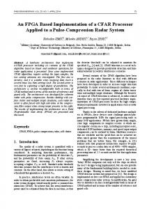
6. Example Application
3. The Image Processing Element The Image Processing Array is composed of 16 identical processing elements. Each element can be thought of as a small DSP specifically intended for image processing algorithms. The processing element is built upon a 16-bit input, 32-bit output datapath, and a RISC-like instruction set composed of 15 instructions. Figure 3 illustrates the structure of the Image Processing Element (IPE), which operates on two’s complements 16bit data and produces a 32-bit output. The IPE receives its data manipulation instructions from the main controller, and operates on pixels stored in its local memory according to the decoded instructions. It also comprises a small coefficient memory which can hold multiplication coefficients, convolution and correlation masks as well as matrix constants. It has two register files which may be used for temporary storage during computation. Once the algorithm execution has been completed, the IPE makes the data and target address available on its output, and informs the output sequencer of its readiness.
4. Implementation The architecture described in the previous section was designed as a soft IP core using VHDL, prior to being embedded with a host processor on the same programmable device. To evaluate the performance of the system, the architecture was first implemented and tested using Celoxica’s RC1000-PP board [8]. This is made up of a single Virtex FPGA with extended memory capability (XCV2000E), and four external memory banks used for frame buffering. The architecture connects directly to a
Figure 5 demonstrates an application which utilises the parallel processor on board the RC1000-PP to pre-process vehicle images for numberplate recognition. The parallel processor removes the image background and unwanted details. It therefore prepares the image for upper layers to locate the plate position, before ‘cutting out’ characters and passing them on to a neural network for classification. At 50 MHz clock frequency, the parallel processor implementation on the FPGA can achieve a throughput of up to 125 Frames/s; whereas the original software application which normally runs on a standard PC achieves 50 Frames/s with a processor clock frequency of 266 MHz. The factor of 2.5 improvement over a CPU which is clocked at 5 times the input frequency is mainly due to the parallelism of the architecture, and its optimised datapath.
7. Conclusion & Further Work Rapid implementation of parallel structures based on FPGAs using VHDL proves to be a very efficient, costeffective and attractive methodology for design verification. New multi-million gate FPGAs [9] with extended memory and fast I/O interfaces made it possible to develop and test a large parallel architecture such as the one described in this paper. Future work will explore the possibility of integrating a host RISC processor into the system so as to complete the processing blocks needed for a complete embedded vision system. This will be an ideal use of System-on-a-Programmable-Chip (SOPC) technology [10], where the host processor is implemented either as a soft or hard core on a high-density Field Programmable Device with sufficiently large amounts of on-chip memories and advanced interfaces.
Acknowledgements This work is funded by the European Commission’s Marie Curie Host Fellowship contract number HPMI-CT-19900055 with NeuriCam S.p.A., Italy.
0-7695-1926-1/03/$17.00 (C) 2003 IEEE
Host Processor (PC) PCI Bus C O M M S
Memory Arbiter & Switches
Memory Banks 0, 1, 2, 3
XCV2000E FPGA: Image Pre-Processing Architecture
Fig. 4. The complete vision system
Performance Characteristics Max Clock Frequency 50 MHz Power Consumption 2.8 W (XPower Estimations) Processing Array 16 IPEs Image Size 256x256 pixels External Memories 5 Mbits Peak Performance 3.23 GOPS Convolution 3x3 88.42 Frames/s Median Filter 62.42 Frames/s Thresholding 666.67 Frames/s 3-Tap FIR Filter 217.39 Frames/s 15-Tap FIR Filter 58.07 Frames/s Correlation 8x8 136.80 Frames/s (64x64 AOI) Forward DCT 70.82 Frames/s Table 1. Performance Characteristics
Unit DMA Channel IPE IPA (16 IPEs) Barrel Shifter Output Sequencer Complete System
FPGA Resources 2,392 Slices 790 Slices 12,967 Slices 101 Slices 36 Slices 16,083 Slices (83%) 128 RAM Blocks (80%)
Table 2. FPGA Resources Phase Design Effort Implementation Synthesis Place & Route
Time 8 Months 2 Months 2.5 Hours 3 Hours
Table 3. Design Efforts
0-7695-1926-1/03/$17.00 (C) 2003 IEEE
Fig. 5. Example Application
References F. Paillet, Design Solutions and Techniques for Vision System on a Chip and Fine-grain Parallelism Circuit Integration, Workshop at the IEEE ASIC / System On Chip Conf., Washington DC, USA, 2000. 2. M. Betke et al, Real-time multiple vehicle detection and tracking from a moving vehicle, Machine Vision and Applications, 12(2), 2000, 69-83. 3. N Yamashita et al, A 3.84 GIPS Integrated Memory Array Processor with 64 Processing Elements and a 2-Mb SRAM, IEEE J. of Solid-State Circ., 29(11), 1994, 1336-1343. 4. NeuriCam, NC1802 Pupilla 640x480-pixel Digital Camera, Datasheet Preliminary Rel. 11/2001. www.neuricam.com 5. P. Athanas & A. Abbott, Addressing the Computational Requirements of Image Processing with a Custom Computing Machine: An Overview, Workshop on Reconfigurable Architectures, IPPS '95, 1-15, 1995. 6. U Ramacher et al, A 53-GOPS Programmable Vision Processor For Processing, Coding-Decoding And Synthesizing of Images, Proc. 27th Eur. Solid-State Circ. Conf., Villach, Austria, 2001, 160-163. 7. T Minami et al, A 300-MOPS Video Signal Processor with a Parallel Architecture, IEEE J. of Solid-State Circ., 26(12), 1991, 18681875. 8. Celoxica, RC1000 Product Information Sheet, www.celoxica.com 9. Xilinx, Virtex 2000-E Datasheet, www.xilinx.com 10. Pat Mead, Investigating the Reality of System-On-a-Programmable-Chip, FPL 2001. 11. Anil Jain, Fundamentals of Digital Image Processing (New Jersey: Prentice Hall, 1989). 1.
0-7695-1926-1/03/$17.00 (C) 2003 IEEE