to support various services that can have very different require- ments .... control PC is used to configure the parameters, stream data, ... Dresden, Tech. Rep.
Short Paper: Flexible GFDM implementation in FPGA with support to run-time reconfiguration Martin Danneberg, Nicola Michailow, Ivan Gaspar, Dan Zhang and Gerhard Fettweis Vodafone Chair Mobile Communication Systems, Technische Universit¨at Dresden, Germany
I. I NTRODUCTION
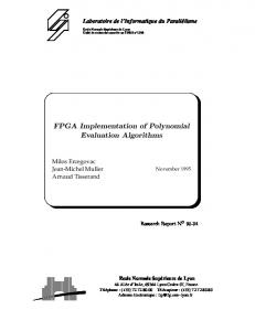
δ0 δ1 ...
M blocks
~gm
of size K
δ0 δ0 δ0 δ1 δ1 δ1 ... ... ...
~ x
+
Fig. 1. Structure of the GFDM modulator.
The fifth generation (5G) of mobile cellular systems needs to support various services that can have very different requirements, e.g., ultra-low latency in the Tactile Internet scenario, low power consumption in large scale machine-to-machine communication and low out-of-band emission in dynamic spectrum access. A physical layer (PHY) with unprecedented flexibility will be of benefit to users because it will allow multiple applications to be addressed efficiently by reconfiguring the modem. Such a flexible PHY necessitates a waveform with many degrees of freedom. From the implementation perspective, it is challenging to achieve flexibility, because it typically entails increased computational complexity of the modulation and demodulation algorithms. This paper contributes with a strategy to implement Generalized Frequency Division Multiplexing (GFDM) [1], demonstrating the feasibility of new schemes. II. P RINCIPLES OF GFDM GFDM is a block based transmission scheme that relies on circularity in the signal structure. The modulator processes blocks of N = KM complex valued data symbols dk,m with k = 0, . . . , K − 1 and m = 0, . . . , M − 1,
~ δm
repeat M times
Index Terms—GFDM, FPGA, implementation, transmitter
d~m
S/P
Abstract—Innovative 5G applications will challenge future cellular systems with new requirements. The OFDM based 4G standard will not be able to address all of them. Generalized frequency division multiplexing is a flexible multicarrier waveform with additional degrees of freedom. This paper presents a strategy towards a flexible FPGA implementation of GFDM, which is reconfigurable at run-time.
K point DFT
{martin.danneberg,nicola.michailow,ivan.gaspar,dan.zhang,fettweis}@ifn.et.tu-dresden.de
(1)
which are distributed across a time-frequency grid that consists of K subcarriers and M subsymbols. Each data symbol is filtered with a corresponding filter � � � � kM gk,m [n] = g (n − mK) mod N · exp j2π n (2) N with n = 0, . . . , N −1. Thus, the prototype filter g[n] is shifted circular in time and frequency. The transmit signal is then given as K−1 −1 XM X x[n] = dk,m · gk,m [n]. (3) k=0 m=0
Lastly, a cyclic prefix (CP) can be added in GFDM for an entire block that consists of multiple subsymbols.
The flexibility of the waveform results from the adjustable parameters K and M and the exchangeable prototype filter g[n]. For example Orthogonal Frequency Division Multiplexing (OFDM) can be seen as a corner case of GFDM, where K > 1, M = 1 and a rectangular filter is used. Figure 1 presents an efficient structure to implement eq. 3 based on [2]. The input data vector d~ = (d0,0 , . . . , dK−1,0 , d0,1 , . . . , dK−1,1 , . . . , dK−1,M −1 ) is divided into M subvectors d~m = (d0,m , . . . , dK−1,m ), which carry the data transmitted in the mth subsymbol. A K point discrete Fourier transform (DFT) is performed, yielding a precoded version of the data ~δm . After the DFT, the subsymbols are processed in parallel. Each vector ~δm carries K samples and is repeated M times, yielding a sequence of N samples, which is then multiplied elementwise with the coefficients of the subcarrier filter ~gm = (g0,m [n])N . The transmit signal ~x is generated by superposition of all M signals. Note that in this realization, the prototype filter is only shifted in time direction, while the upconversion to the subcarrier frequency k happens implicitly with the DFT of the data [2]. III. I MPLEMENTATION A PPROACH GFDM has been previously implemented [3], exploiting the large number of near-zero coefficients in the frequency response of the filter to reduce the necessary multiplications [4]. However, this first approach requires to perform a oddnumbered DFT in FPGA, which is less efficient than powerof-two based transforms. The odd numbers originate from the fact that GFDM modulation mathematically is a Gabor expansion [5] and as such, the parameter M needs to be odd. Otherwise, considering a linear zero-forcing or matched filter receiver, the system may face severe noise enhancement. The method described in Section II requires K-point DFTs instead
Fig. 2. Screen-shot of the multi-rate-diagram implementation in the LabVIEW Communication Design Suite. The actual resource usage without the DFT corresponds to the total of: registers (2%), DSPs (1%), Block RAMs (37%), LUTs (5%), and slices (10%).
of M -point DFTs and hence it can be implemented with even transform lengths. Figure 2 shows how the GFDM modulator was implemented using the multi-rate diagram (MRD), which is a tool that enables fast prototyping with the LabVIEW Communications Systems Design Suite. While this particular design is limited to K = 512 and M = 5, the concept can be extended for a larger range of the parameters. The design consists of five main functional blocks, driven by the address counter in (A), which increments when a new data sample is available at the input of the diagram. The range of the counter is k = 0, . . . , K − 1. A second address signal m = 0, . . . , M −1 counts the subsymbols, i.e. increases every time k reaches the max value. The block (B) performs a K point DFT. In (C), M = 5 parallel branches process K = 512 samples each. In each branch, the transformed data is multiplied with the filter coefficients of the prototyoe filter, which are stored in M look-up tables (LUTs) that can be reconfigured during operation. The multiplexers (MUXes) in (D) are controlled by m and route the signal parts to five memory banks in such a way, that the signal at the output of the diagram obtains a block-circular strcuture. At this point, the MUXes are hard-wired for M = 5 and will be replaced a configurable interconnect matrix in the future. The memory banks in (E) have the purpose of accumulating the signal contributions from all m subsymbols in the data block. They are flushed whenever a new block starts, i.e., m = 0. Finally, the delay chains and the MUX in (F) facillitate a serial to parallel conversion. This implementation is flexible because the parameters K, M and the filter coefficients can be changed during run-time. Besides the DFT operation, that can be changed in powers of 2, changing K is a memory operation, where only parts of the address range are used in the subsequent parts. The number of blocks M can be changed by switching on or off the respective blocks. Still, the maximum values are limited by the capabilities of the FPGA, particularly the number of available block RAM.
IV. P ROTOTYPE P LATFORM The GFDM waveform modulator was implemented on the National Instruments USRP-RIO 2953R. This software defined radio has a built-in Kintex-7 FPGA (XC7K410T) and a radio
fronted with two channels. In this setup, the USRP-RIO is connected to a control PC via the NI PXIe-PCIe8371 card. While the GFDM modulation is performed in the FPGA, the control PC is used to configure the parameters, stream data, capture the modulated signal and evaluate the results. The proposed algorithm relies considerably on the large amount of block memory that is available in the Kintex-7, because the entire pulse shaping filter and the transmit signal needs to be stored in the internal block memory. For the final design, the parameters Kmax = 2048 and Mmax = 21 are considered, which means that the memory banks for the pulse shaping filter and the accumulator have a length of 21x2048x32 ≈ 1.4 Mbit each. A transceiver with one modulator and one demodulator needs at least 5.6 Mbit, which is already around 20% of the available resources. V. C ONCLUSIONS New waveforms require a higher complexity compared to the simple DFT/IDFT of OFDM. As the hardware advances it allows to use more resources in modern systems, e.g. block RAM. However, if this investment in the increased complexity is pursued, than the benefit is a flexible modulator, which can produce a waveform with properties that are individually adapted to the requirements of it’s specific usage scenario. VI. ACKNOWLEDGEMENTS The authors thank National Instruments for supplying all necessary software and hardware tools to implement the prototype and for providing unconditional technical support. R EFERENCES [1] N. Michailow et. al, “Generalized Frequency Division Multiplexing for 5th Generation Cellular Networks,” IEEE Transactions on Communications, vol. 62, no. 9, pp. 3045–3061, 2014. [2] I. Gaspar et al., “GFDM Transceiver using Precoded Data and Lowcomplex Multiplication in Time Domain,” under minor review, 2015. [3] Ainoa Navarro et. al, “GFDM Base Transceiver Implementation,” TU Dresden, Tech. Rep., 2014. [Online]. Available: https://mns.ifn.et.tudresden.de/Research/Projects/Pages/5GNOW.aspx [4] I. S. Gaspar, M. N., A. Navarro Caldevilla, E. Ohlmer, S. Krone, and G. Fettweis, “Low Complexity GFDM Receiver Based On Sparse Frequency Domain Processing,” in Vehicular Technology Conference, 2013. VTC Spring 2013, IEEE 77th, 2013. [5] M. Matth´e, L. L. Mendes, and G. Fettweis, “GFDM in a Gabor Transform Setting,” IEEE Communications Letters, vol. 18, no. 8, pp. 1379–1382, 2014.