Journal of Systems Architecture. Vol.57, No.2, 2011, pp.214-227.
Architectures and Optimization Methods of Flash Memory Based Storage Systems Yuhui Deng, Jipeng Zhou Department of Computer Science, Jinan University, Guangzhou, 510632, P. R. China Email:
[email protected] ;
[email protected];
Flash memory is a non-volatile memory which can be electrically erased and reprogrammed. Its major advantages such as small physical size, no mechanical components, low power consumption, and high performance have made it likely to replace the magnetic disk drives in more and more systems. However, flash memory has four specific features which are different to the magnetic disk drives, and pose challenges to develop practical techniques: (1) Flash memory is erased in blocks, but written in pages. (2) A block has to be erased before writing data to the block. (3) A block of flash memory can only be written for a specified number of times. (4) Writing pages within a block should be done sequentially. This survey presents the architectures, technologies, and optimization methods employed by the existing flash memory based storage systems to tackle the challenges. I hope that this paper will encourage researchers to analyze, optimize, and develop practical techniques to improve the performance and reduce the energy consumption of flash memory based storage systems, by leveraging the existing methods and solutions.
Keywords: Flash memory, Energy efficient, Solid State Disk, Disk drive, Storage system 1. Introduction Flash memory is a non-volatile memory which can be electrically erased and reprogrammed. Its major advantages such as small physical size, no mechanical components, low power consumption, and high performance have made it likely to replace magnetic disk drives in more and more mobile and embedded systems (e.g. digital camera, MP3 player, mobile phone etc.), where either size and power or performance are important [10, 58, 68, 71]. In the past decade, NAND flash densities have been almost doubling each year since 1996 [9, 33]. Samaung has delivered NAND flash memories with capacity ranges from 64MByte to 4GByte [85, 86]. A 32GByte flash drive, which integrates 16 2GByte flash memory chips, is also available on the market [86]. Flash memory is also much cheaper than the volatile memories such as SDRAM. For example, 1Gbit of NAND flash memory costs 3.75$, while the same size of low power SRAM and fast SRAM cost 320$ and 614$, respectively [71, 86]. Due to the increased capacity and decreased price, flash memory is expected to be widely used in high-end computer systems as an important and promising storage media. Flash memory can play two roles in the existing computer system architecture: (1) As an extension to RAM, and a layer between RAM and the magnetic disk drives. (2) Replacing the magnetic disk drives as block-level storage media. The memory hierarchy in current computer architectures is designed to take advantage of data access locality to improve overall performance. Each level of the hierarchy has higher speed, lower latency, and smaller size than lower levels. Magnetic disk drives are millisecond devices, DRAM are nanosecond devices, and flash memory chips are microsecond devices. It seems that flash 1
Journal of Systems Architecture. Vol.57, No.2, 2011, pp.214-227.
memory can play as an intermediate layer (e.g. a non-volatile cache) between the DRAM and the magnetic disk drives in terms of the memory hierarchy. Magnetic disk drives have been the preferred media for data storage for several decades. However, the architecture of disk drives currently is facing two challenges. The first one is performance. Disk drives are highly complex systems consisting of electronic and mechanical components. Due to the slow mechanical latency, the disk I/O subsystem has been repeatedly identified as a major bottleneck to system performance in many computing systems. Although the performance of disk drives has been experiencing 40% growth per year, the performance gap of RAM to disk drive has been widened to 6 orders of magnitude in 2000 and will continue to widen by about 50% per year [80]. The second one is energy consumption. Fan et al. [27] investigated the power consumption of the major components within a typical server. They reported that the peak power of one X86 CPU, one Motherboard, one PCI expansion slot, one IDE disk drive, one fan, and one DDR memory are 40W, 25W, 25W, 12W, 10W, 9W, respectively. From a power standpoint, it seems one disk drive is not a problem. Even the addition of several dozen disk drives would hardly be a concern. However, if hundreds or thousands of disk drives are put together, it will quickly become a big headache. One example shows the storage subsystem accounting for 27% of the energy consumed in a data centre [26]. To worsen the situation, this fraction is swiftly increasing as storage requirements are rising by 60% annually [29].The characteristics of flash memory including high performance, low energy consumption, and small size make them the potential storage media in comparison to the traditional disk drives. Therefore, this paper attempts to explore the opportunities and challenges of how to employ the flash memory as a block-level storage media. Flash memory has four specific features which are different to magnetic disk drives. The first one is that flash memory is erased in blocks, but written in pages. Each block consists of a number of pages. The second one is erasing before writing. It indicates that a block has to be erased before writing data to the block. The third one is that a block of flash memory can only be written for a specified number of times. The fourth one is that writing pages within a block should be done sequentially or incrementally [41, 87]. This is called Sequentiality of Programming (SOP). In a Multi Level Cell (MLC) flash memory, two or more bits are programmed in one cell. Among the bits, a lower bit is denoted as the Least Significant Bit (LSB) and an upper bit is denoted as the Most Significant Bit (MSB). The LSB pages within a block should be programmed before the MSB pages. Random page address programming is prohibited. In this case, the definition of LSB page is the LSB among the pages to be programmed. Therefore, LSB doesn’t need to be page 0. Please note that sequential page programming does not have to be consecutive page programming. Therefore, a sequence of page 1, page 5, and page 8 is acceptable, but a sequence of page 1, page 8, and page 5 will incur lots of fail bit. Flash memory is usually accessed by embedded systems as a raw medium or indirectly through a block-oriented device. In other words, the management of flash memory is carried out by either software on a host system (as a raw medium) or hardware/firmware inside its device [38]. Therefore, there are two kinds of approaches to overcome the hardware limitations of flash memory [34]. One is designing a new flash file system [3, 4, 21, 46, 49, 63, 66, 73, 89]. The other one is using the traditional file systems (e.g. FAT and Ext2), and wrapping the flash memory to mimic a block-level storage device. Consequently, the algorithms and functionalities used to handle the characteristics of flash memory (e.g. erasing before writing and the limited life span) can be integrated into either a file system [49, 77] or the firmware inside a flash memory device [51, 59]. Gal and Toledob [34] wrote a comprehensive survey about the algorithms and data structures for flash memory. They reviewed flash-specific file systems including log-structured file systems[49], research-in-motion file system[73], Journaling Flash File System(JFFS)[3], Yet Another Flash File System (YAFFS)[4], Trimble file 2
Journal of Systems Architecture. Vol.57, No.2, 2011, pp.214-227.
system[66], Microsoft flash file system[89], Norris flash file system [21], and some other commercial embedded file systems. However, due to the compatibility with traditional file systems, the second solution is more popular and widely used in products. In contrast to their work, this paper attempts to review the architectures, technologies, and optimization methods involved in the flash memory devices. The major objectives of this survey are: (1) To understand the flash memory technology, and basic design concepts of flash memory based storage systems. (2) To create awareness among the researchers about state-of-the-art optimization methods developed for the flash memory based storage systems in the community. (3) To help discover more effective ways to improve performance and reduce energy consumption of the flash memory based storage systems. (4) To create a vision about future directions/challenges for the flash memory based storage systems. The remainder of the paper is organized as follows. Overview of the flash memory is introduced in Section 2. Section 3 describes the flash memory based storage systems including system architecture, logical-to-physical address mapping, wear-leveling, garbage collection, and power-off recovery. Section 4 discusses the architecture, performance pattern and the corresponding optimization methods, and energy consumption and conservation of Solid State Disk (SSD). Section 5 concludes the paper with remarks on the contributions of the paper. 2. Overview of flash memory
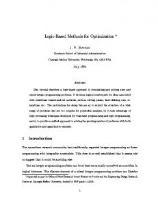
(a) NOR Flash (b) NAND Flash Fig. 1 Cell architecture of flash memory [25, 56] There are two major types of flash memory, which are available on the market, following different logic schemes: namely NOR and NAND. The cell architecture of NOR flash and NAND flash is different. NOR flash arranges cells in parallel between two bit lines. NAND flash serially connects the cells along the bit line. Fig.1 illustrates the cell architecture of two different flash memories [25, 56]. Each cell of a NOR flash is a MOSFET transistor which has two gates. There is a control gate (CG) on the top. A floating gate (FG) insulated from its surroundings by an insulating oxide material is below the CG. The FG resides between the CG and the MOSFET channel. The electrons injected onto the FG are trapped because the FG is isolated by the insulating material. Unlike the NOR flash, the basic cell of a NAND flash is a MOSFET transistor with a floating gate. Charge is injected into this gate during writing, and released during erasing. The organization of NAND flash cells reduces much of the decoding overhead found in other memory technologies. However, accessing one individual cell has to go through the other cells in its bit line in terms of Fig. 1 (b). This adds significant noise to the reading. It also brings challenges to writing since the adjacent cells in the line should not be disturbed. For erasing, all cells on the same bit line have to be 3
Journal of Systems Architecture. Vol.57, No.2, 2011, pp.214-227.
erased. The NOR flash memory, which employs a standard memory interface, is byte accessible and can be adopted as execute-in-place memory. It is designed for efficient random access. It is mainly used for programmable read-only memory (PROM) and erasable PROM (EPROM) replacement. It has separate address and data buses like EPROM and static random access memory (SRAM). Compared with the NOR flash memory, NAND flash memory has faster erasing and write times, simpler interface, along with higher data density. Therefore, NOR flash memory is well suited for code storage and execute-in-place (XIP) applications, while NAND flash memory is a better candidate for data storage [45]. As explained in the introduction Section, the traditional disk drives are facing both performance and energy consumption challenges, and the NAND flash could replace the magnetic disk drives as the major storage media. Therefore, this paper focuses on the NAND flash. The flash memory in the following sections denotes NAND flash memory. Chang and Kuo[10] summarized the characteristics of NAND and NOR flash memory listed in Table 1. Table 1. Characteristics of NAND flash memory and NOR flash memory NAND
NOR
Density
High
Low
Read/write
Page-oriented
Bitwise
XIP
No
Yes
Read/write/erase
Moderate/fast/fast
Very fast/slow/very slow
Cost per bit
Low
High
NAND flash memory can use Single-Level-Cell (SLC) technique or Multi-Level-Cell (MLC) technique. For the SLC flash memory, one cell represents one bit (two states), whereas MLC doubles or even triples the memory density of SLC. This is possible because of the charge storage in the floating gate, which allows for subdividing the amount of stored charge into small increments. When this is coupled with the superior retention characteristics of the floating gate, it is possible to accurately determine the charge state after a long period of time. Unfortunately, the decreased separation between charge states incurs a higher sensitivity to cell degradation in comparison to the SLC [56]. Therefore, SLC flash memory is faster, more reliable, and has a longer life span than MLC. However, for the same-sized die, MLC is cheaper and can provide larger storage capacity than that of SLC flash. Thus, MLC NAND flash memory is suitable for low-bit cost and high-density applications, while SLC NAND flash memory is a good candidate for high-performance applications [13, 41]. However, MLC has a shorter lifespan which degrades every time when data is written to the cell. It is estimated that the native lifespan of an SLC cell is around 100,000 cycles, but it drops to around 10,000 cycles with two bit MLC cells and as low as 1,000 cycles on a three bit cell. There are algorithms to extend the lifespan such as MLC charge-placement algorithms [56], but the bottom line is that lower-capacity SLC has a much longer life span [76]. Table 2 summarizes the characteristics comparison of SLC and MLC NAND flash memory. Table 2. Characteristics comparison of SLC and MLC NAND flash memory SLC
MLC
Density
Low
High
Performance
High
Low
Reliability
High
Low 4
Journal of Systems Architecture. Vol.57, No.2, 2011, pp.214-227.
Life span
Long
Short
Cost per bit
High
Low
Flash planes
logic
Row decode
address
Spare area
Col. decode
Control and
Data area
NAND Flash array
One block
One page
8/16 bit bus I/O
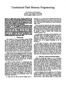
Data register
Fig. 2 Architecture of a typical flash chip A NAND flash memory is composed of flash plans. The plans can be independent with its own buffer to hold data, thus allowing simultaneous operations for higher performance, although they compete for the package pins. Each plan consists of a fixed number of blocks, where each block is further divided into a number of pages and each page has a fixed-size main data area and a spare data area. The data area is for the storage of data, and the spare area stores the corresponding LBA, ECC, and other information. Data on NAND flash memory is read or written at the page level, and the erasing is performed at the block level. A static RAM buffer holds data before writing or after reading, and data is transferred to and from this buffer via an 8 bit or 16 bit wide bus. Fig. 2 shows the architecture of a typical flash chip [25]. Data transfer consists of two parts. The first part is transferring data over the external bus to or from the data register. The second part is between the data register and the flash arrays. Table 3 summarizes the parameters of five different NAND flash memories from four manufacturers [2,30,42,85, 88]. Table 3 indicates a non-uniform access latency for read. It shows that a sequential read in flash memory is three orders of magnitude faster than a random read. This is consistent with what Chen et al. [12] have observed. Table 3 also illustrates that the endurance cycle of flash memory could be as low as 10K. This may not be a good news for using the flash memory in enterprise storage systems. Table 3. Characteristics of typical NAND Flash Memories Manufacturer
Samaung
Intel
AMD
FUJITSU
Type
K9NBG08U5A
JS29F16G08FANB1
Am30LV0064D
MBM30LV0128
Capacity
4G x 8 Bit
2G x 8 Bit
8M×8Bit
16M×8Bit
Page Size(Byte)
(2K + 64)
(2K + 64)
(512 + 16)
(512 + 16)
Block Size(Byte)
(128K + 4K)
(128K + 4K)
(8K + 256)
(16K + 512)
25µs(Max)
N/A
10µs(Max)
Random Read
25µs(Max)
Serial Read
50ns(Min)
25ns(Min)