260
Area Efficient Time to Digital Converter (TDC) Architecture with Double Ring-Oscillator Technique on FPGA for Fluorescence Measurement Application Mahantesh P Mattad 1, Hansraj Guhilot1, Rajanish K Kamat2 [1]
Dept. of Electronics & Communication, K.L.E. Society’s College of Engineering & Technology, Udyambag, Belgaum – 590008, INDIA. (E-mail:
[email protected],
[email protected]) [2]
Department of Electronics, Shivaji University, Kolhapur – 416 004, INDIA. (E-mail:
[email protected] Fax: +91-231-2692333, Phone: +91-231-2609204)
Keywords- Time to Digital Converter, Tapped Delay Line, Field Programmable Gate Array, Fluorescence, Vernier delay Line
The present paper is organized as follows. After introducing the theme, Section II explains the prior art and describes the motivation behind the work. Section III portrays the concept of Time to Digital Converter (TDC) using Double Ring Oscillator topology. Nutt’s principle is used to obtain both long measurement range as well as fine resolution. Design and implementation on Xilinx Spartan 3 is detailed in the following section. The section IV also discusses the results of implementation. The last section concludes the development.
I. INTRODUCTION Measurements of time intervals between two or more physical events are frequently required in many science and industry applications. In research based applications, the cost of designing and manufacturing a custom CMOS ASIC is often prohibitive. This poses even greater problem since the development process invariably involves two, three or more iterations of the design [2, 3]. ASIC- based approach offers high speed and precision but the design and fabrication process is expensive, complicated and time-consuming. Therefore the researchers resorts to the FPGA-based design that offers more flexibility, lower cost and faster time to market. There are instances reported in the literature of such implementations on low-cost chip family; e.g. Altera Cyclone kit costs ~$200[4].
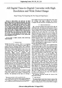
Figure1 Experimental setup to measure delayed chlorophyll fluorescence in photosynthesis
Abstract—We present an area efficient Time to Digital Converter (TDC) yielding a high resolution of nearly 10ps. The TDC architecture reported in this paper comprises of coarse measurement using system clock and two controllable oscillators for fine resolution measurement. The reported improved resolution is attributed to the difference in their frequencies. One of the main features of the implementation is its prototyping on a low-cost FPGA.
Though there are good numbers of applications of TDC, in the present paper we report a fluorescence measurement application that necessitates high resolution. The basic principle is shown in Figure 1 that portrays the photon counter that needs TDC of high resolution [1]. The above mentioned TDC can be realized using FPGA, while the rest of the blocks are realized in the ASIC paradigm. The main advantage of migrating the TDC in the FPGA paradigm is making the best of its configuration and reconfiguration capabilities.
II.
PRIOR ART
The literature survey reveals many techniques for FPGA based implementation of TDCs. First such implementation has been reported by Kalisz. In this work Tapped Delay Lines (TDL) technique was adopted and resolution of the order of 200ps has been reported. In the above mentioned work, though there is advantage in terms of less conversion time, however the same is not efficient in terms of silicon real estate and requires large number of flip-flops. Yet another resort to
978-1-4244-9477-4/11/$26.00 ©2011 IEEE
261
alleviate the area inefficiency is the ‘Interpolation method’, which also gives high resolution along with used long fullscale range. The Long full scale range is provided by coarse counter driven by reference clock while high resolution which is obtained by fine interpolators, however again suffers from errors like non-linearity of interpolators and quantization error [4]. Other techniques such as tapped delay lines or Vernier delay line concept, are popular in the FPGA paradigm, though with inherent drawbacks such as large area consumption and unpredictable Place and Route delay which is attributed to the time delay from gates themselves put together [2]. The limitation of one such architecture implemented in [2] is it’s difficulty in real device realization, since frequencies of the ring oscillators are faster than what most of the FPGA and I/Os are rated for. Moreover, direct measurement of ring oscillator period is difficult, because of loading of ring oscillator by a buffer, variations induced by placement, routing delays to the device pin, all results in mismatch between the measured and true period [3]. In the backdrop of the above developmental scenario pertaining to the TDC implementations, our work reports improved implementation by resorting to the conception of the dummy load. Further the manual floor plan incorporated in the flow has been advantageously used for controlling the place and route delay. With the background of the theme in place now we report the basics of the Double Ring Oscillator based TDC. III. DOUBLE RING OSCILLATOR BASED TDC
Tresolution = Tslow – Tfast
(3)
To measure error we first enabled slow oscillator at the positive rising edge of the error TI, and the fast oscillator at negative edge. These oscillators are connected to counters and phase detector. Phase detector output indicates coincidence of fast and slow clock edges. Figure 5 shows timing diagram for the slow and fast clock. Coincidence between phases of slow and fast clock can also be seen in figure5 which is quit ideal. Practically, the possibility of coincidence between rising edges of fast and slow clocks is very less, normally they cross over. The error due to cross over is less than the resolution and is given by. (4) Errorcrossover< Tresolution In our implementation, two binary counters are driven by two oscillators as shown in figure 6. The size of the counter1 (driven by slow clock) is decided by considering two factors. First, maximum possible error that can occur during coarse measurement. It is easily noticeable that the maximum amount of error is nearly equal to (but less than) the period of reference clock. Second, the oscillation period of slow ring oscillator. Size of counter2 (driven by fast clock) is decided by two factors. First, maximum possible time difference between falling edge of the Error TI (shown in figure 5) and immediate rising edge of slow clock. Maximum possible time difference is nearly equal to (but less than) the period of slow clock. Second, the period difference between slow clock and fast clock, i.e. the resolution, because fast clock has to overtake the slow clock in steps of Tresolution.
The double ring oscillator based TDC resorts to the Nutt’s The numbers stored in counters n1 and n2 are used to find principle, the analytical treatment of which may be found in [2]. In normal method of time interval measurement the Error TI as given in equation 5. reference clock is used for coarse counter which is simple a (5) Error TI= (n1-1) Tslow - (n2-1) Tfast binary counter. Coarse count is basically equal to number of clock cycles multiplied by the period of the reference clock i.e. nTref. The resolution is limited to reference clock period Tref. There are two possible errors as shown in figure2. A novel Errors finder block is shown in figure3, which will give Time interval error1 and error2 occurred in the coarse measurement. Behavioral simulation of Errors finder is shown in figure4. In Fine measurement, these errors are measured and Reference added/subtracted with the coarse count to obtain exact time clock interval value. It can be understood easily by following mathematical equations. Coarse
Texact = nTref ± errors
(1) Error1
With respect to figure2, equation (1) yields Texact = nTref + error1 – error2
(2)
To measure errors we have used Vernier principle. There are two controllable oscillators with slightly different frequencies ffast and fslow, and the incremental resolution is given by equation 3.
Error2
Figure2 .Measurement of time interval Retrieved from [2]
262
IV. DESIGN, IMPLEMENTATION AND RESULTS There are many ring oscillator circuits with control inputs, few of them mentioned in [2] and [3] which have been taken as the basis for the present work and improved by incorporating the dummy load. The schematic of ring oscillators is as shown in figure7, drawn using ISE 9.2 schematic design entry tool. This tool also provides manual floor planning, place and route facility. We undertook manual floor planning so as to get different delays and hence dissimilar oscillation frequencies. Figure 8 shows editable floor plan for Spartan-3 FPGA (xc3s50-4-pq208). Figure3. Schematic of Errors finder Dummy loads
Dummy loads
Figure4 Behavioural simulation of Errors finder Figure7 Double ring oscillator schematic Error TI
Post route Simulation results shown in figure7, which shows fast oscillator running at a period of 1964.0ps and slow oscillator running at 1974.0ps. Thus the difference in delay gives a resolution of the order of 10ps.
Slow clock
Fast clock
Figure5 Timing diagram for the slow clock, fast clock
Figure8 Editable floor plan for ring oscillators
Figure6 General Block diagram of vernier principle
After covering the basic principle and alaytical treatment the rest of the paper describes the design and implementation.
Figure9 Post route simulation of Ring oscillators
263
Oscillating period of ring oscillators which are shown in post route simulation (figure 9), changes after connecting phase detector and counters. This is due to the drift in the frequencies because of loading effect. In order to maintain the original period differences and there by resolution, there are two solutions. First one is to edit the floor plan, thereby varying Place and Route delay. Second solution is to use the loading effect again, i.e. by loading oscillators with dummy loads, such as buffer, flip-flop etc. Connecting (unused) pad along with the load is a must, otherwise that logic is considered as unused and trimmed off while mapping by Xilinx software. We have used both the solutions inorder to yield better results. Phase detector schematic is given in figure 10. Output of AND2b1 gate is high when it detects “10” sequence. Output of the phase detector is used to control the oscillators and counters. Behavioural simulation of phase detector is also shown in figure11. In Accordance with the equation 4, the crossover error is less than 10 pico-seconds.
IV. CONCLUSION It is difficult to get sub-100 pico-second resolution in Time to Digital Converter in the FPGA paradigm. We resorted to the manual floor planning and thus could alleviate the Place and Route delay difference by using two ring oscillators with slightly different in oscillating frequencies. The period difference of these two ring oscillators gives 10ps resolution. Simulation results show better resolution than earlier works especially reported in [2] and [3]. Since two ring oscillators and phase detector consume four to five CLB’s, our implementation yields high area efficiency and consumes less silicon real estate. Work is in progress to use the improved technique of time to digital conversion reported here for the measurement of delayed chlorophyll fluorescence in the photosynthesis process. ACKNOWLEDGMENT We would like to thank the PG Section (VLSI Design Embedded System), Department of Electronics Communication, KLE Society’s College of Engineering Technology, Belgaum for helping us with the tools equipments.
and and and and
REFERENCES [1] [2] [3]
Figure10 Schematic of phase detector
Figure11 Behavioral simulation of phase detector
[4]
Hansraj Guhilot and Rajanish K. Kamat “All nMOS 10-T AQRC for Monolithic Chlorophyll Fluorescence SPAD Sensor”, IEEE transactions 2010 Lin, Min-Chuan, "FPGA-Based High Area Efficient Time-To-Digital IP Design", IEEE TENCON 2006 Sachin S Junnarkar, Paul O'Connor and Rejean Fontaine “FPGA based self calibrating 40 picoseconds resolution, wide range Time to Digital Converter”, IEEE Nuclear Science Symposium Conference Record, 2008 Sudeshna Dasgupta “Study of FPGA-based TDC Architectures for ICAL”, INO Collaboration Meeting, IIT Kharagpur, 5thMay 2010