approximately 30â between the array and a Molex. (Molex Inc., Lisle, IL, USA) connector [ll]. Laser cuts were made between the traces in order to increase the.
Proceedings of the 25' Annual International Conference of the IEEE EMBS Cancun, Mexico * Scptember 17-21,2003
Assembly-Ready Brain Microelectrode Arrays T. Fofonoff', S.Martells2,I. Hunter'
' Bioinstrumentation Laboratory, Department of Mechanical Engineering, Massachusetts Institute of Technology (MIT), Cambridge, MA, USA 2NanoRobotics Laboratory, Department of Computer Engineering, Ecole Polytechnique de Montreal (EPM), Campus of University of Montrbal, Montreal, Canada Abstract-The capabilities of wire electrical discharge machining as a method of constructing microelectrode arrays are highlighted, and new assembly procedures based on this technique are presented. Particular attention is paid to the design of the connection between the mechanical array and the front-end electronics, a problem that is common to the construction of all microelectrode array assemblies. Keywords-Microeleetrode array, neuroprosthesis, intracortical recording, electrical discharge machining, EDM 1. INTRODUCTION
The prospects of neural prostheses are rapidly improving. Together with advancements in medical and biological research, innovations in electronics and micromanufacturing have increased the feasibility of brainmachine interfaces. Although various methods of creating a link to the functions of the brain are currently under investigation [I], microelectrodes are the simplest and most successful technology used today in capturing action potentials of individual neurons. By simultaneously recording signals from several small groups of neurons, one is able to track intended movements with an accuracy that varies with the number of electrodes or channels in use [2]. Cochlear implants in clinical use operate with as few as six channels. Future vision and motor prostheses, however, due to the higher level of complexity inherent in their function, are expected to require an increased number of channels and electrodes, possibly on the order of hundreds or thousands. This significant increase in the required number of recording sites has led to the development of microelectrode array assemblies. Although the development of low-power electronics and software for neural interfaces continues to receive much attention, the mechanical aspects of these devices may provide the largest bamers for wide-spread clinical use [3]. Several techniques are currently used in the development of microelectrode array assemblies for use as scientific tools in neuroscience. These include, for example, silicon-based approaches [4],[5], and polymer-based approaches [6]. It has yet to be seen, however, whether any of the current methods can deliver the yields and tolerances necessary, in an automated fashion and at an acceptable expenditure, in order to bridge the gap to clinical use. It is highly desirable for a clinical implant to have telemetry capabilities, thus eliminating the need for
0-7803-7789-3/03/$17.00 02003 IEEE
percutaneous connectors. Much work has been undertaken with this goal in mind [7]-[9]. Even in a laboratory setting, a wireless implant would reduce the probability of infection, reduce the noise and artifacts caused by the movement of the connector cable, and enable more freedom of movement of the animal. Wireless implants would also move the digitizing of the signals into the body, thereby reducing attenuation and increasing the signal-to-noise ratio compared to the tethered case. It has been suggested that the front-end electronics be mounted in die form directly onto the back of the array using a flip-chip or a wire-bonding technique [7]. This would have a positive effect on the signal-to-noise ratio, as it is desirable to amplify the signals as close to the sources as possible. It is also advantageous to convert the signals into digital form as soon as possible, thus reducing the number of connections that must linked to the electronics performing peak detection and data transmission. Although one electronic die attached to the reverse size of a microelectrode array would likely be manageable, mounting several components directly onto the back of an array may not be possible due to space limitations. Additionally, these components would have to be well encapsulated, as microelectrode arrays are normally insetted beneath the dura mater that surrounds the brain. A flexible ribbon cable, therefore, is required to route the signals from the microelectrode array to other electronics positioned in the region of the implant, but outside the dura mater.
11. METHODOLOGY A. Array Fabrication by Electrical Discharge Machining
Electrical discharge machining (EDM) makes use of the erosive effects of an electrical discharge to remove material from the workpiece. It is a forceless process in which there is no contact between the workpiece and the machining electrode. EDM, in general, occurs in a tightly-controlled environment and uses computer numerically controlled (CNC) stages in order to perform positioning with micrometer precision. Fig. 1 shows a microelectrode array that was wire electrical discharge machined in a hexagonal or honeycomb pattern from a piece of titanium-aluminum-vanadium alloy (Ti90-A16-V4). Each electrode is 250 pm from its six neighboring electrodes. Electrical discharge machining,
1937
Fig. 2. A microelectrode array that has been epoxied into a palyimide substrate and then freed from its base by wire electrical discharge machining. The inter-electrodespacing of this 8 x 8 array is 508 pm. Fig. I . SEM image of an lldlelectrode hexagonal microelectrcde array that was electrical discharge machined fmm a single piece of titaniumaluminum-vanadiumalloy.
C. Connection to the Array Assembly
when combined with a chemical etching technique, has proven capable of producing electrodes with lengths of 5 nun, widths of 40 pm, and inter-electrode spacings of 250 pm [IO]. This technique has also been shown capable of creating exceptionally detailed features and arrays of electrodes with varying lengths. In addition to its CNC nature, the use of wire EDM allows for the use of virtually any metal, including stainless steel, titanium alloy, or platinum-iridium alloy, for example. This can produce a valuable strength and biocompatibility advantage over the use of other materials and methods, allowing, for example, electrodes to be built with a smaller width dimension and volume while keeping the same strength characteristics.
Connection to microelectrode array assemblies requires special attention because it is a potential site of electrical and mechanical failure. In order to increase design turnaround time, previouiily constructed assemblies were assembled by soldering 1:he backs of the electrodes onto pads that surrounded through-holes in the cable [ I l l . In the rendering shown in Fig. 3, this connection is replaced by a gold bonding technique. The design consists of a speciallymachined array, which makes use of EDM capabilities to create a structure in which a l o x IO array of electrodes, with an inter-electrode s,pacing of 400 pm, is spread out on the upper surface in order to allow for the placement of a 2.5 mm x 3.5 mm eloctronic die. The structure is constructed with a transparent epoxy and has been ground flat in preparation for the: gold bonding step.
E. Mechanical Assembly of the Array Structure Ground
The conductive components of microelectrode array assemblies must be structurally connected in order to be inserted into the brain at a known spatial resolution. In the case of electrical discharge machined arrays, an insulating substrate must either be formed around or attached to the array structure in order to hold the electrodes in their machined configuration. Epo-Tek 301 epoxy (Epoxy Technology Inc., Billerica, MA, USA) was chosen for this task due to its strength characteristics and its biocompatibility. A polyimide substrate is used to keep the epoxy in place by surface tension while it is curing [Ill. Ledge features are machined as part of the electrodes in order to provide a stop for the polyimide substrate when it is placed over the array. Shorter, electrical discharge machined stumps, positioned around the electrodes, have alternatively been used to hold the substrate in place at the desired electrode length. Fig. 2 shows an array of electrodes that has been freed from its base by wire EDM.
Substrate
13lectronic Die
Pads for
Electrodes
Fig. 3. Rendering of a configuration that could be used in assembling a microelectrodearray that has bi=n wire electrical discharge machined. The stmctllre is encapsulated with a clear epoxy and ground flat, revealing pads that are accessible for gold bonding to a rectangular die that contains the front-end electronics.
1938
Additional traces could be added to the design shown in Fig. 3 in order to route pads from the die to larger pads machined into the substrate. These larger pads would then be used for attachment of a ribbon connector cable. The traces shown in Fig. 3 could be extended much farther in order to accommodate a larger die. Alternatively, for a flipchip process, the array would similarly be machined in order to place the back ends of the electrodes at locations that correspond to the padlocations on the die.
Testing has been done in order to verify that the Epo-Tek epoxy can indeed be ground in order to allow for gold-bonding or ultrasonic attachment of a foil. Fig. 5 shows pads that havc becn ground using diamond wheels and fine grain sandpapers. The method was found to produce smooth pads. It also scales well, as it could potentially he done on several arrays in parallel.
D. Connector Cable Design An earlier version of the connector cable, manufactured from polyimide-based flexible printed circuit board (flex-PCB), consisted of sixty-four parallel 50.8-pm-wide copper traces, spaced 152.4 pm apart, extending for approximately 30” between the array and a Molex (Molex Inc., Lisle, IL, USA) connector [ l l ] . Laser cuts were made between the traces in order to increase the flexibility of the cable. Even with these cuts, however, the cable was found to have a shape memory and to exert restoring forces that were troublesome during implantation. The follow-up design highlighted here eliminates the need for supporting polyimide in the cable, and instead calls for the cable to he fabricated from a highly ductile gold foil which is bonded to the back side of the array ultrasonically or using conductive epoxy before it is machined. The entire cable is then encapsulated with vapor-deposited parylene C, a material capable of providing adequate insulation with minimal thickness. Initially, the gold and parylene ribbon cable will he tested in joining the microelectrode array to a connector. The method could later be expanded to incorporate the use of electronics mounted in die form. Fig.4 shows a schematic of the steps involved in the construction of the cable. The method benefits from joining the cable to the workpieces in bulk form prior to machining in order to eliminate the need for subsequent connecting. Id foil is bonded tu workpipirces sonically or using conductive epoxy.
2. Traces are machined in the gold by liver ablation.
3. An insulating substrate is forme an the back ride of the array warkpicce from polyimide and epoxy. 4. me microelectrode array and
connecta are machined by EDM Fig. 4. Schematic showing the steps involved in fabricating the flexible ribbon cable.
Fig. 5 . Image of electrodes that have been encased in epoxy and then ground flat in order to provide goad attachment pads.
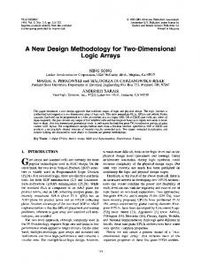
Initial testing of parylene has found it to be a suitable choice for the encapsulating material. And, because parylene is already used in insulating the electrodes in order to achieve desirable electrode impedance values [ I l l , its deposition could be combined with the encapsulating step. Laser ablation of the electrode tips would then be left as the last step in the fabrication process. More testing is required in order to verify the flexible ribbon cable design. The microelectrode array structure shown in the Fig. 3 rendering was wire electrical discharge machined, and an image of it is shown in Fig. 6 below. The I O x I O array has an inter-electrode spacing of 400 pm and fans out in order to surround a 2.5 mm x 3.5 mm die. The rows of pads in the stmcture are spaced 250 pm apart. A substrate with holes 400 pm apart is epoxied onto this array. After curing, the array is freed from its base by wire EDM, and then the back side of the array is completely encased with epoxy and ground flat so that it resembles the rendering in Fig. 3. The epoxy could altematively be applied before the array is removed, and then the entire hack of the structure could be ground. Also, several arrays could be processed in parallel, with one single substrate being placed over a number of arrays. After the substrate is secured in place, the space behind the arrays would be filled with epoxy and left to cure. Following this, the arrays could be ground flat all at once, and then separated to form a multitude of assemhlyready components.
1939
REFERENCES J. P. Donoghue, “Connecting cortex to machines: recent advances in brain interfaces,” Namre New. Rev., vol. 5, pp.
Fig. 6 . Image of a 10 x IO microelectrode a m y that war. electrical discharge machined from titanium-aluminum-vanadium alloy. This array has a configuration identical to that rendered in Fig. 3. It has an interelectmde spacing of400 pm, and the electrodes fan out in order to surround a 2.5 mm x 3.5 mm electronic die. The rows of pads in the Smcture (corresponding to the base of the electrodes in the above image) are spaced 250 pm apan.
V. CONCLUSION
The capabilities of wire electrical discharge machining have been highlighted, and EDM-based techniques have been demonstrated as viable means of manufacturing microelectrode arrays. A design for a microelectrode array assembly suitable for attaching a gold-bonded or flipchipped electronic die has been presented, as well as manufacturing tests and preliminary results. A design for a gold and parylene ribbon cable for use io joining an array assembly with its front-end electronics has also been presented. In combination with the application of epoxy and a grinding step, the presented EDM-based techniques show the potential for manufacturing several assembly-ready components in parallel.
ACKNOWLEDGMENT The authors wish to thank N. Hatsopoulos of the Department of Organismal Biology and Anatomy at the University of Chicago and J. Donoghue of the Department of Neuroscience at Brown University for their contributions to this work.
1940
1085-1088,2002. M. D. Sermyq N. G. Hatsopoulos, L. Paninski, M. R. Fellows, and 1. P. Donoghue, “Instant neural contml of a movement signal,” Norwe, vol. 416, pp. 141-142, 2002. K. S. Guillory and B. W. Hatt, “Electrode arrays for large-scale neural interfaces,” Proc. 2nd Join1 EMBUBMES Con!, Houston, TX, USA, Oct. 23-:!6,2002, pp. 2107-2108. K. Jones, P. Campbell, and R. Nonnano. “A GlasdSiliwn Composite Intracoitical Elecacde Army,” Ann. Biomed. Eng., vol. 20, pp. 42343’1, 1992. Q. Bai, K. D. Wise, and D. I. Anderson, “A High-Yield Micmassembly Smichue For Thne-Dimensional Microelectrode Arrays,” IEEE Trans. Biomed. Eng,, vol. 47, pp. 281-289,2000. D. R. Kipke, D. S. Pellinen, and R. J. Vdter, “Advanced neural implants using thin..film polymers,” IEEE Int. Symp. on Circuits andSyslems, vo1.4, pp IV-173-N-I76,2002. S . Martel, N. Hatsapoulas, 1. Hunter, J. Donoghue, I. Burgnt, I. Malsek, C. Wiseman, and R. Dyer. “Development of a wireless brain implant: The Telemetric Electrode Army System (TEAS) project: Proe. 23rd Am. Int. Con! of the IEEE Eng. in Med. and Bio. SE.. Istanbul, Turkey, Oct. 25-28, 2001, pp. 35943597. K. D. Wise, “Wireless implantable micmsystems: coming breaWlmughs in health care,” S p p . on V U 1 CirnriLr Dig. of Tech. Popers, pp. 106-109,2002. 1. F. Hetke, 1. C. Williams, D. S. Pellinen, R. 1. Vetter, and D. R. Kipke, “3-D silicon probe array With hybrid polymer interconnect far chronic cortical recording,“ Prm. 11 IEEEEMBS Con/: on Neur. Eng., Capri Island, Italy, Mar. 20-22, 2003. .. DD. 181-184. [IO] T. Fofonoff, S . Mmel, C. Wiseman, R. Dyer, 1. Hunter, N. Hatsopoulos, and 1. Donoghue,“A highly flexible manufacturing technique for micrrielectmde anay fabrication,” Proc. 2nd Joint EMBWBMES Con!, Houston, TX, USA, Oct. 23-26, 2002, pp. 2 107-2 108. [ l l ] T. Fofonoff, C. Wiseman, R. Dyer, J. MalUek, I . Burpen, S. Martel, 1. Hunter, N. Hatsopoulos, and I. Donoghue, “Mechanical assembly of B microelectrode array for use in a Wireless intraconical recording device,” Proc. 2nd Ann. Inl. IEEE-EMBS Special Topic Con! on Microtech. in Med. and Bio., Madison, WI, USA, May 24,2002, pp. 269-272.