31st Annual International Conference of the IEEE EMBS Minneapolis, Minnesota, USA, September 2-6, 2009
PDMS-Based Conformable Microelectrode Arrays with Selectable Novel 3-D Microelectrode Geometries for Surface Stimulation and Recording Liang Guo and Stephen P. DeWeerth Abstract— A method for fabricating polydimethylsiloxane (PDMS) based conformable microelectrode arrays (MEAs) with selectable novel 3-D microelectrode geometries is presented. Simply recessed, conically recessed, exponentially recessed, and protruded-well microelectrodes have been fabricated on the MEA with a diameter as small as 10µm. 3-D microelectrode geometry parameters (recess depth, recess slope & profile, and protrusion/planar) can be controlled independently during fabrication. Exponentially and conically recessed microelectrodes are promising in chronic stimulation applications, such as neural prostheses, for their production of a uniform current density profile during stimulation, which can minimize stimulationinduced tissue burning and electrode corrosion. Protruded-well microelectrodes potentially provide a closer and sealed contact to the target tissue surface, avoiding current leakage during stimulation and thus achieving better stimulation efficiency in both charge delivery and spatial specificity.
I. INTRODUCTION In recent years, neurophysiology research and neural prosthesis development have created a strong demand for conformable MEAs to be used as intimate, adaptable neural interfaces. Thus, efforts have been made to fabricate MEAs on compliant substrates, such as PDMS, to provide the device capability of conforming to the tissue surface in the pursuit of a uniform and tight contact on the target tissue surface [1], [2], [3], [4]. In chronic stimulation applications, it has been reported that charge density and charge per phase are the critical factors responsible for stimulation-induced neural damage [5]. It has also been shown that, for non-recessed disk electrodes, peak current density builds up at the electrode-insulator edges (commonly known as “edge effect”) [6]. Theoretical analyses [7] and experimental measurements [8] have demonstrated that excess current density at the electrode edges can be reduced or eliminated by recessing the electrode into the carrier, creating a welled electrode, and by radially varying the recess. Suesserman et al. reported that an exponentially recessed electrode could produce the most ideal charge injection profile and that the charge injection profile produced by a conically recessed electrode was also fairly uniform. However, it has been very difficult in fabricating such uniform-profile electrode geometries, especially This work was supported by the NIH Grant EB006179 L. Guo is with the Wallace H. Coulter Department of Biomedical Engineering, Georgia Institute of Technology and Emory University, Atlanta, GA 30332 USA
[email protected] S. P. DeWeerth is with Faculty of the Wallace H. Coulter Department of Biomedical Engineering, Georgia Institute of Technology and Emory University, Atlanta, GA 30332 USA
[email protected]
978-1-4244-3296-7/09/$25.00 ©2009 IEEE
at the micrometer scale, which has significantly limited the application of such advantageous electrodes. We have addressed the issue of making uniform current density profile microelectrodes by fabricating different 3D microelectrode geometries on PDMS-based conformable MEAs. Our fabrication method provides PDMS-based MEAs with simply recessed, conically recessed, exponentially recessed, or protruded-well microelectrodes at 10µm resolution. II. METHODOLOGY A. Basic MEA Fabrication Process Briefly, in our fabrication process, a PDMS base layer is spun on a glass substrate; gold features are patterned using a lift-off process; sacrificial posts are formed using negative photoresist right on top of the electrodes and contact pads where openings are to be made; the device is encapsulated with a second thin PDMS layer; the sacrificial posts are removed to expose the electrode and contact pad openings; and finally the device is peeled off the glass substrate. As an example, stepwise processes for fabricating MEAs with protruded-well microelectrodes are shown schematically in Fig. 1 and are described in detail below. 1) Preparing Glass Slide and PDMS: A cleaned glass ˚ non-stick gold layer primed slide is coated with a 250A ˚ by 100A titanium in an electron beam evaporator (CVC Products, Inc.) to facilitate device peeling-off in the end (Step 1 in Fig. 1). PDMS (Sylgard® 184, Dow Corning) elastomer base is mixed with curing agent at 10 : 1 weight ratio. A PDMS base layer is formed by spin-coating the de-aired PDMS mixture onto the gold-coated glass slide. The spin speed and duration are adjusted depending on the desired device thickness. The sample is then cured on a hotplate at 90℃ (Step 2 in Fig. 1). 2) Lift-off Patterning Gold Traces: The sample is first briefly treated in oxygen plasma to activate the cured PDMS surface [9]. Immediately following this treatment, positive photoresist (Shipley Megaposit™ SPR™ 220 7.0) is spun on at 1500rpm for 30 seconds with a ramp rate of 300rpm/s, and cured on a hotplate at 90℃ (Step 3 in Fig. 1). The resulting photoresist layer is ∼12µm. The sample is then patterned with a UV exposure energy dose of 700mJ/cm2 at 365nm i-Line, developed in developer (Shipley Microposit® MF® -319) for about 160 seconds. Finally, the resulting photoresist negative mask is flood-exposed with the same dose to enable subsequent lift-off in its developer (Step 4 in Fig. 1). A hold time of at least 120 minutes is required before starting depositing gold to allow water, which is necessary
1623
Step 1:
TABLE I UV EXPOSURE CONFIGURATIONS FOR CREATING SACRIFICIAL POSTS
Step 2:
WITH DIFFERENT SIDEWALL PROFILES
Sacrificial Post Sidewall Profile
Step 3:
Contact Type between Mask and Sample
Step 4:
vertical tapered
hard 1mm distance
†
Step 5:
exponential
1mm distance
†
†
Step 6:
‡
Step 7:
Step 9:
Step 10:
Step 11: Final Device Non-stick layer
Photoresist for lift-off patterning gold
PDMS
21 14 ± k × 5/3 ‡ (k = 0, ±1, ±2, ...) 14 ± k × 5/6 ‡ (k = 0, ±1, ±2, ...)
A 1mm-thick glass slide is placed between the photomask and the sample. These exposure doses need to be calibrated based on the exposure equipment used.
5) Removing Sacrificial Posts to Open Electrodes and Contact Pads: To remove the sacrificial posts, the sample is immersed in acetone for about 10 minutes, and then the electrode area is rinsed briefly with acetone stream. Confirmation that all electrodes have been opened can be achieved through inspection under a microscope; subsequent acetone soaking and rinsing is applied as necessary until all electrodes are opened (Step 10 in Fig. 1). 6) Detaching the Device from Glass Slide: The completed device is peeled off its glass slide while immersed in isopropanol, which helps to reduce stress and prevent the film from self-adhesion (Step 11 in Fig. 1). Finally, the device is soaked in de-ionized water for 24 hours to remove any chemical residues that may get involved during fabrication.
Step 8:
Glass slide
Exposure Energy (mJ/cm2 for 1µm)
Gold
Photoresist for making sacrificial posts
Fig. 1. Illustration of stepwise fabrication processes for PDMS-based MEAs with protruded-well microelectrodes.
to complete the photo-reaction, to diffuse back into the photoresist mask. The sample is then placed in an electron ˚ titanium and 5000A ˚ gold both beam evaporator for 300A ˚ deposited at 1A/s. (Step 5 in Fig. 1). After deposition, the sample is soaked in the corresponding photoresist developer MF-319 to dissolve the photoresist mask and lift off excess gold film, leaving only the desired gold features (Step 6 in Fig. 1). 3) Defining Sacrificial Posts: Following brief treatment in oxygen plasma, a thick layer of negative photoresist (NR58000, Futurrex, Inc.) is spun onto the sample (Step 7 in Fig. 1). The photoresist layer is patterned to leave sacrificial posts right on top of each gold electrode and contact pad where an opening is to be made (Step 8 in Fig. 1). 4) Spin-coating the Second PDMS Layer for Encapsulation: Following oxygen plasma treatment, the second PDMS layer is spun on to encapsulate the device at 5000rpm for 150 seconds with a ramp rate of 1000rpm/s. The uncured sample is left at room temperature for one hour, baked on a 60℃ hotplate for one hour, and then baked in a 90℃ oven for another hour. The resulting encapsulation thickness is ∼10µm, except at the surroundings of the sacrificial posts (Step 9 in Fig. 1).
B. Achievement of Different 3-D Microelectrode Geometries Different 3-D microelectrode geometries are achieved by carefully controlling two critical parameters during the fabrication process: (a) the micro-shape of the sacrificial posts, and (b) the conversion between hydrophobicity and hydrophilicity of both the PDMS and sacrificial post surfaces. We employ Aperture Diffraction to manipulate the UV light intensity profile during the exposure process of the NR5-8000 for making sacrificial posts with a tapered profile. Furthermore, we found that the sidewall profile of the sacrificial post could be controlled by adjusting the UV exposure energy to create sacrificial posts with different sidewall slopes, as well as exponentially curved sidewall profiles (TABLE I). By varying the parameter k in TABLE I within a certain range, different sidewall slopes can be made. This enables the molding of microelectrode openings with complimentary geometries. Naturally, the surface properties of cured PDMS and NR58000 are both hydrophobic, but they can be temporarily converted to hydrophilic upon brief oxygen plasma treatment. Brief oxygen plasma treatment of the PDMS surface before passivation is necessary to ensure good adhesion between the two PDMS layers. Our results showed that the temporary hydrophilicity of PDMS surface could last more than one day when left in air, in spite of the decrease in strength with time, and that of the negative photoresist NR5-8000 we used for making the sacrificial post could only last less than two
1624
TABLE II K EY PARAMETERS FOR FABRICATING DIFFERENT 3-D MICROELECTRODE GEOMETRIES ON PDMS- BASED MEA S Electrode Geometry
Sacrificial Post Shape
Sacrificial Post Height
Material Surface Property PDMS (substrate) NR5-8000 (sacrificial post)
simply recessed
vertical
any
convert to hydrophilic
back to hydrophobic
conically recessed
tapered
low
convert to hydrophilic
convert to hydrophilic
exponentially recessed
exponential
low
convert to hydrophilic
convert to hydrophilic
protruded-well
any
depend on well depth
convert to hydrophilic
convert to hydrophilic
hours. This observation was used to separately control the surface properties of PDMS and NR5-8000 in TABLE II before spinning on the encapsulation PDMS layer. By manipulating the thickness of the PDMS encapsulation layer and the sacrificial post parameters with respect to height, sidewall profile, and surface property, we can independently control the 3-D microelectrode geometry parameters in terms of recess depth, recess slope & profile, and protrusion/planar. TABLE II gives the key process parameters for fabricating different 3-D microelectrode geometries on PDMS-based MEAs. III. RESULTS A. Fabrication Results
(a)
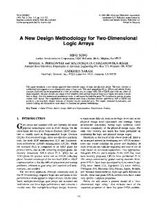
As a demonstration, Fig. 2 shows a five-electrode MEA and four different 3-D microelectrode geometries on four of such MEAs. Distant scanning electron microscope (SEM) images of exponentially recessed microelectrodes appeared to be similar to those of conically recessed ones [Fig. 2(b)(ii)], so a close-up image is shown in Fig. 2(b)(iv). During experiments for fabrication process evaluation, our fabrication method achieved gold traces as thin as 10µm wide, and electrode openings as small as 10µm in diameter (data not shown). And thickness of the MEA could be easily set from tens of micrometers to more than one millimeter. B. Surface Contact Performance of Protruded-Well Microelectrodes Protruded-well microelectrodes appear to be more promising because of their combined capability of improving surface contact and producing a uniform current density profile during stimulation. So, in this section, we focus on testing the performance of protruded electrode wells when they make contact with a surface in solution (to mimic the biological environment where the MEA will be used). An MEA (with its glass slide attached for ease of handling and observing) was immersed in de-ionized water in a Petri dish. As shown in Fig. 3(a), an air bubble was trapped in each of the electrode wells due to hydrophobic property of the PDMS material. These bubbles can be avoided by brief oxygen plasma activation of the PDMS surface in advance. A 25 x 25 x 0.2mm thin glass slide (0.3g) was placed over the electrodes, which were then inspected under an optical microscope. The contact between the thin glass slide and the MEA surface became firm when water in-between was squeezed out as the glass slide settled down onto the MEA surface. Also, the interfacing process squeezed those
(b) Fig. 2. PDMS-based MEA with different 3-D microelectrode geometries. (a) A five-electrode MEA. The electrode openings have a diameter of 80µm and a minimum spacing of 230µm. The device thickness is approximately 80µm. (b) SEM images of different 3-D microelectrode geometries: (i) simply recessed, (ii) conically recessed, (iii) protruded-well, and (iv) exponentially recessed (close-up).
air bubbles out of each electrode well. This was verified after the thin glass slide was removed later. Fig. 3(b) shows the interfacial contact between the protruded electrode wells and the thin glass slide. It can be seen that each electrode well formed a perfect seal (the light ring encircling each electrode) on the glass surface, without any inward bending. Moreover, it was observed that when the thin glass slide was initiated a slight displacement with respect to the MEA, the electrode wells still sealed to the original sites, despite being stretched to irregular shapes (image not shown). This experiment showed that, as a result of the “sticky” property
1625
(e.g., cochlear implants and epiretinal prostheses). Moreover, while potentially providing a closer and sealed contact to the target tissue surface and thus achieving better stimulation efficiency in both charge delivery and spatial specificity, the protruded-well microelectrodes [Fig. 2(b)(iii)] can also be incorporated with an exponentially or conically recessed slope, making such electrodes promising in (chronic) neural surface stimulation applications that require high spatial selectivity and minimal stimulation-induced tissue damage (e.g., spinal-cord surface stimulation). In the near future, we plan to use electrogenerated chemiluminescence (ECL) imaging experiments [10], [11], [12] to verify the uniform current density profile of these novel microelectrodes. Also, we are planning to test the selective stimulation efficiency of the protruded-well microelectrodes on rat spinal-cord surface stimulation experiments.
(a)
V. ACKNOWLEDGMENTS This research was supported by the NIH Grant EB006179. R EFERENCES
(b) Fig. 3. Optical microscope images for surface contact performance of protruded-well microelectrodes. (a) The MEA was immersed in de-ionized water. An air bubble was trapped in each of the electrode wells. (b) Interfacial contact between protruded-well microelectrodes and a thin glass slide placed over. Each electrode well formed a good seal (the light ring encircling each electrode) on the glass surface, without any inward bending.
of the PDMS material and the special geometry of the electrode wells, the protruded-well microelectrodes could create a highly isolated micro-environment when contacting a surface. IV. DISCUSSION Stimulation-induced neural injury is an important issue in clinical applications involving chronic neural stimulation. The burning of the tissue is primarily caused by excess charge density and charge per phase [5]. In order to minimize such damage, on the electrode design side, the goal is to reduce or eliminate the non-uniformity of stimulation current density at the electrode-tissue interface. Recessed electrodes were reported to reduce the excess current density at the electrode edges [7], [8]. Exponentially and conically recessed microelectrodes were considered to produce a uniform current density profile during stimulation [8]. Our achievement of exponentially and conically recessed microelectrodes [Fig. 2(b)(ii) and (iv)] as small as 10µm in diameter on a conformable PDMS film has great promise in improving neural prostheses that involve chronic neural surface stimulation
[1] M. Maghribi, J. Hamilton, D. Polla, K. Rose, T. Wilson, and P. Krulevitch, “Stretchable micro-electrode array [for retinal prosthesis],” in 2nd Annual International IEEE-EMB Special Topic Conference on Microtechnologies in Medicine & Biology, May 2002, pp. 80–83. [2] S. P. Lacour, C. Tsay, S. Wagner, Z. Yu, and B. Morrison, “Stretchable micro-electrode arrays for dynamic neuronal recording of in vitro mechanically injured brain,” Proc. of the 4th IEEE Conference on Sensors, pp. 617–620, 2005. [3] M. Schuettler, S. Stiess, B. V. King, and G. J. Suaning, “Fabrication of implantable microelectrode arrays by laser cutting of silicone rubber and platinum foil,” J. Neural Eng., vol. 2, pp. S121–S128, 2005. [4] K. W. Meacham, R. J. Giuly, L. Guo, S. Hochman, and S. P. DeWeerth, “A lithographically-patterned, elastic multi-electrode array for surface stimulation of the spinal cord,” Biomedical Microdevices, vol. 10, no. 2, pp. 259–269, April 2008. [5] D. B. McCreery, W. F. Agnew, T. G. Yuen, and L. Bullara, “Charge density and charge per phase as cofactors in neural injury induced by electrical stimulation,” IEEE Trans. Biomed. Eng., vol. 37, no. 10, pp. 996–1001, October 1990. [6] J. Newman, “Current distribution on a rotating disk below the limiting current,” J. Electrochem. Soc., vol. 113, pp. 1235–1241, December 1966. [7] J. T. Rubinstein, F. A. Spelman, M. Soma, and M. F. Suesserman, “Current density profiles of surface mounted and recessed electrodes for neural prostheses,” IEEE Trans. Biomed. Eng., vol. 34, no. 11, pp. 864–875, November 1987. [8] M. F. Suesserman, F. A. Spelman, and J. T. Rubinstein, “In vitro measurement and characterization of current density profiles produced by nonrecessed, simple recessed, and radially varying recessed stimulating electrodes,” IEEE Trans. Biomed. Eng., vol. 38, no. 5, pp. 401–408, May 1991. [9] B. H. Jo, L. V. Lerberghe, K. M. Motsegood, and D. J. Beebe, “Threedimensional micro-channel fabrication in polydimethylsiloxane (pdms) elastomer,” Journal of Microelectromechanical Systems, vol. 9, no. 1, pp. 76–81, 2000. [10] C. M. Pharr, R. C. Engstrom, R. A. Tople, T. K. Bee, and P. L. Unzelman, “Time-resolved imaging of current density at inlaid disk electrodes,” J. Electroanal. Chem., vol. 278, pp. 119–128, 1990. [11] R. G. Maus, E. M. McDonald, and R. M. Wightman, “Imaging of nonuniform current density at microelectrodes by electrogenerated chemiluminescence,” Anal. Chem., vol. 71, pp. 4944–4950, 1999. [12] R. M. Wightman, C. L. Curtis, P. A. Flowers, R. G. Maus, and E. M. McDonald, “Imaging microelectrodes with high-frequency electrogenerated chemiluminescence,” J. Phys. Chem. B, vol. 102, pp. 9991– 9996, 1998.
1626