acoustic material signature (AMs), the transducer output voltage along the axial lens travel. This signature ... ELECTRONICS LETTERS 4th January 1996 Vol. 32.
The material-dependent Rayleigh velocity is obtained via the acoustic material signature (AMs), the transducer output voltage along the axial lens travel. This signature is composed of a number of AMS periods, denoted by Az,, from which the Rayleigh velocity v, is readily computed [4]. A typical AMS trace is shown in Fig. 1, characteristic of the [loo] orientation on a cubic Silicon surface at 370MHz. In time it was recognised [3] that an upper limit existed on measuring the Rayleigh velocity at high frequencies [3]. New AMS parameter: Recently it was pointed out that the acous-
tic material signature may contain additional information that is not limited to these constraints [5]. The new AMS parameter Az, also indicated in Fig. 1 measures the axial separation between the maxima of the focal plane and the first AMS peaks of the transducer output voltage travelling along z the lens axis. Az, overcomes the restrictions imposed on Az,.
P /
z
\
4 - 1 0 0 MHz
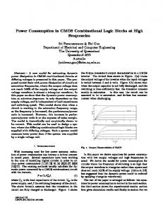
and frequency range. In fact, AzM extends the useful range of the classical acoustic metrology mode to higher velocity materials at high frequencies where the number of Az, periods is severely restricted, as may be deduced from Fig. 2 [3]. The accuracy to which AzM can be measured suffers considerably compared with the experimental determination of Azw Only one value is available for determining the first maxima spacing hMwhereas several sharp minima dips of the AMS curve over which b, can be averaged to improve accuracy are usually available. It should be noted that eqn. 1 does not tak.e into account the axial length of the lens system in that the calculated value of AzM may at high frequencies extend well beyond the physical working distance of the lens. Conclusions: A new material characterisation parameter AzM has been added to the AMS family in an acoustic microscope that extends the useful range of the acoustic micro- metrology mode to higher velocity materials at high frequencies. M[easured data point sets at two different frequencies are in close agreement with a simple empirically derived equation. The precisioa with which Az, can be measured is somewhat reduced compared with the AMS period Azw 11 October 1995 Electronics Letters Online No: 19960008 R.D. Weglein (6317 Drexel Avenue, Los Angeles, CA 90048-4703, USA)
0 IEE 1996
References R.D.: ‘A model for predicting acoustic material signatures’, Appl. Phys. Lett., 1979, 34, (3), pp. 179-181 WEGLEIN, R.D.: ‘SAW dispersion and film-thickness measurement by acoustic microscopy’, Appl. Phys. Lett., 19’79, 35, (3), pp. 215217 WEGLEIN, R.D.:‘Acoustic micro-metrology’, IEEE Trans., 1985, SU32, (2), pp. 225-234 PARMON, w., and BERTONI, H.L.:‘Ray interpretation of the material signature in the acoustic microscope’, Electron. Lett., 1979, 15, (21), pp. 684686 HIRSEKORN, s., and PANGRAZ, s.: ‘Materials clharacterization with the acoustic microscope’, A. P. L. Tech. Dig., 1994, 64, (13), pp. 1632-1634 KIM, J.O , and ACHENBACH, J.D.: ‘Line focus acoustic microscopy to measure anisotropic acoustic properties of thin films’, Thin Solid Films, 1992, 214, pp. 25-34 KIM, J.o., and ACHENBACH, J.D.: ‘Line focus acoustic microscopy measurements of thin-film elastic constants’ in THOMPSON, D.O., and CHIMENTI, D.: ‘Review of progress in QNDE’ (Plenum Press, 1993), 12B, pp. 1899-1906 WEGLEIN,
2
4 6 8 10 12 Rayleigh velocity VR, mmlps Fig. 2 Variation of N,, and AzM against Rayleigh velocity vR with f r e quency [MHz]as a parameter
A experimental Az, data at 225MHz experimental Az, data at 370MHz Computed AzM curves are from eqn. 1 N,,, = maximum number of AMS periods Az, that can be obtained with a given acoustic lens This point is illustrated by an examination of Fig. 2, that shows the variation of the maximum possible number N,,, of AMS periods on the left [3] and the 1st maxima spacing Az, against the Rayleigh velocity and at several indicated frequencies on the right. Note that, e.g. at 1000MHz, N,,, 2 1 cannot be achieved for v, >bmm/ps. Nine experimental AzM data points measured at 370MHz [l] covering a wide Rayleigh velocity range are shown, as well as two measurements at 225MHz [6, 71. Both sets of data closely follow the empirical eqn. I, except at low Rayleigh velocities where vR < 3 . 5 d p s .
AZM E (3/4)Xf/[l - &l - CKZ’)] (1) where hj = v / i the wavelength at frequencyf, v, = 1 .4831nm/ps at 24”C, the water coupling fluid velocity, x = v/v,, and a is an empirical parameter. It is conjectured that a depends largely on the acoustic lens material, e.g., sapphire or quartz. a = 2 is an excellent fit to the experimental data that was acquired with c-axis sapphire lenses of spherical and cylindrical shape at 370 and 225MHz, respectively. That a may be material dependent evolves from the observation of several Az, data points at 5OMHz (not presented here). Using a spherical fused quartz lens required a substantially different a for good agreement. AzM in eqn. 1 is observed to scale with frequency, a fact that is illustrated in Fig. 2 by the encircled data point near v, = S d p , which was frequency scaled from the measured point at 370 225MHz. The point is seen to fall squarely on the 225MHz curve of eqn. 1. Discussion: The addition of Az, to the AMS family serves several
important functions in nondestructive material micro-characterisation. AzM complements the frequency and velocity dependence of the AMS period Az,, in that it provides an additional parameter by which materials may be characterised over an extended velocity
ELECTRONICS LETTERS
4th January 1996
Vol. 32
BILCO: built in testing method for combinational logic circuits D.M. Harvey Indexing terms: Built in serf test, Combinational circuits, Logic circuits The testing of digital logic circuits has become quite complex owing to miniaturisation and its associated increase in circuit function per unit area. Methods have been devised for testing ASIC products and, latterly, board level products. A new method (BILCO) is presented for probing asynchronous combinational logic circuits using a novel development of scan path principles.
Scan path methods for testing digital circuits: :Scan path methods were developed for increasing the access to internal circuit nodes. Early methods concentrated on building the test function into each individual circuit. This has recently been augmented with the introduction of boundary scan testing, which allows both circuit self testing and system interconnection testing.
No. 1
31
The scan path methods are applicable when building self-test into sequential circuits. The Huffman model for a synchronous stored state circuit can easily be modified to include scan path circuitry [I]. This permits fully automatic circuit testing when required as well as normal circuit operation. A number of methods exist for the generation and analysis of test patterns. A built in self-test (BIST) circuit will generate input test patterns, often a PRBS, and analyse test output results, usually by signature analysis [2]. These BIST functions can be implemented using linear feedback shift registers or by the correct configuration of built in logic block observers (BILBOs) [3]. AH these techniques apply to Huffman type circuits but have shortcomings when applied to combinational circuits. inputs
v,
In
combinational logic Yl-out yn in
Ynout
outputs
TEST/NOT_NoR2MAL = 1, test vectors are entered via the scan input. The Yn-OUT test data are held by the D-type flip-flop precedmg the MUX. Apply external inputs to the combinational logic and observe external outputs, after allowing tme for propagation delays to settle. To hold the new intermediate data Yn-IN, put TEST-HOLD = 1 to store the values in the FMCs. To store this data in the D-type flip-flop succeedmg the MUX, switch TEST/ N O T N O R M A L = 0, and apply a single clock pulse. All new Yn-IN values generated by the test will now be ready for clocking out along the scan path, but as a bonus they also drive the Yn-OUT inputs. The external outputs can be observed with these new values if required. To read the Yn-IN stored values, put TEST/NOT-NORMAL = 1, and clock results out via the scan output. If a series of tests are being performed, new test inputs can be scanned in simultaneously. To switch back to normal operation simply switch TEST-HOLD = 0 and TEST/NOT-NORMAL = 0.
clock testlnot -normal
presented which not only allows circuits to operate in a combinational manner, but also allows test data to be scanned into and out of the circuit when required for test purposes. A circuit is presented which has been designed using the asynchronous principles of fundamental mode design [4]. The design allows monitoring of combinational circuits with only a minor influence on the circuits’ intended operation. This treatment amounts to the addition of two extra gate delays in the data path of each node incorporating this testability feature.
built-in logic combinational observer (BILCO)
BILCO operation: The basic structure of the BILCO circuit is
shown in Fig. 2. During normal operation TEST-HOLD and TEST/NOT-NORM A L = 0. Data are piped through the fundamental mode circuit (FMC) and multiplexer (MUX). A test sequence is as follows: When TEST-HOLD = 0 and 32
!
I
!
f I
1
z
1 1
I I
I
I
I
; l-4
1 I
I I
I I I 1
I
1
:
:
:
I
I
I
4
I
I
I I
I
3
I
I I
H I 1
I
I
I I
I I
1 1
I
I
I
:
I
I
5 6 1 4
4
I I
I I
I I
I
l
l
1
1
I
I
1
I
r!--I
I
l
l
I
I
I
1 2 1 1174131
Fig. 3 Specification for fundamental mode circuit (FMC)
Fundamental mode circuit speci3cation and design: Fig. 3 shows a
specification for the fundamental mode circuit (FMC). To store Yn-IN in the FMC, TEST-HOLD = 1, producing Yn-HD, which is a held version of Yn-IN. The state tables for this circuit are shown in Tables 1 - 3. Table 1: Input state table for Yn-IN TEST-HOLD 1
I
I I
0
I
I
1s
14
I
I
14
I 6
0
-
0
-
10
14 I?
1 t l
11
01
12
0
11
Table 3: Implication table 2 Ives I 3 yes
4 yes
lyes 13-5Ino
13-5/no
I
2
3
4
5
The possible combinations can be graphically shown as a combmational polygon whch results m the best state reduction of 1, 2 and 3 into a new state 1, and 4, 5 and 6 into a new state 4. The reduced state tables are shown in Tables 4 and 5.
1 of
I I I
I
state assignment
Conventional scan path testing: Fig. 1 shows a typical scan path
arrangement. To operate as a normal sequential circuit the control line TEST/NOT-NORMAL = 0, and data are routed directly from Yn-IN to Yn-OUT via the MUX and D-type flip-flop. To test Huffman type circuits, data can be scanned in with the TEST/ NOT-NORMAL = 1, and applied to the combinational circuit by switching back to normal mode. Applying a single clock cycle will then store the new Yn-IN data. These test results can then be scanned out as the next test inputs are scanned in. By the provision of an extra control line TEST-HOLD, rearrangement of the scanpath, and a fundamental mode circuit design for holding or transmitting test data, BILCO can be realised.
I I
I
00 Simple methods for combinational circuit testing: A new method is
Fig. 2 Basic structure circuit
1
test-hold Yn-HD
Scan path testing applied to combinational circuits: If a conventional scan path design is included for controlling and observeing nodes embedded in a combinational circuit, its implementation could be as shown in Fig. 1. The previously combinational circuit now becomes a modified Huffman type, in which each event is synchronised to the system clock. A multiplexer (MUX) enables data to be scanned into and out of the circuit in test mode, and allows data to pass via the D-type flip-flops in normal mode. The D-type flip-flop forms an obstacle to normal combinational circuit operation as it requires a clock to pass data from its input to its output. The circuit is not only slowed by the clock rate, but is no longer truly combinational.
clock testlnot-normal. test -hold ’
I 1
I
f :
Yn-ln
Fig. 1 Typical scan path arrangement
I I
Table 4 Input state table for Yn-IN TEST-HOLD 00 01 11 10 1 1
11
11
14
14
14
14
0
10
10
ELECTRONICS LETTERS
-
4th January 7996
Vol. 32
No. 7
0 1
0
0 0
10 I1
10 I1
0
10
10
I
I
I
11 I1
I
X I
I
The resulting equations are: Y = y.TESTHOLD + Yn-IN.NOT-TEST-HOLD YnHD =y which can be realised as the circuit of Fig. 4. This structure can then be incorporated into Fig. 2 to realise test-per-scan built in self-test [5].
Introduction: Fault detection for analogue circuits (both at the wafer-probe stage or in production testing) is typically performed using a fault dictionary in which the actual measured response is compared with the precalculated response of the fault-free circuit. This comparison however is complicated by the presence of VLSI manufacturing tolerances on the circuit parameters, which creates ambiguity regions where no unique decision isan be taken for a given measured response. To make a selection, current practice is to use arbitrary decision windows (e.g. 10 01” 25%) around the fault-free circuit performance (both the voltagl:/current value and time) to decide whether a tested circuit is classified as fault-free or not [I]. The contribution of this Letter is to present an optimal fault detection criterion that takes into consideration the actual statistics of tolerances and mismatches on the analogue circuit parameters, and that minimises the overall decision error. The technique will be illustrated with experimental analogue fault detection results.
RF
Conclusions: A method of testing combinational circuits using scan path techniques has been presented. The BILCO design permits internal nodes to be driven to a test value, while their intermediate outputs are sampled and stored by an asynchronous circuit. The result is an efficient method for testing which leads to only a minor degradation in normal circuit operation. Acknowledgments: The author wishes to thank C. A. Hobson for
introducing him to asynchronous design many years ago. 0 IEE 1996 16 October 1995 Electronics Letters Online No: 19960012 D.M. Harvey (School of Electrical Engineering, Electronics and Physics, Liverpool John Moores University, Byrom Street, Liverpool, L3 3AF, United Kingdom)
References C.: ‘Status of IC design-for-testability’, British Telecom
Technol. J., 1989, 7, pp. 4 4 4 9 C.R., and SALUJA, K.K.: ‘A tutorial on built-in self-test - part i: Principles’, IEEE Des. Test Comput., 1993, 10, (l), pp. 73-82 KONEMAN, B , MUCHA, J., and ZWIEHOFF, G.: ‘Built-in logic block observation technique’. Proc. IEEE Int. Test Conf., 1979, pp. 3741 HILL, F.J., and PETERSON, G.R.:‘Computer aided logical design with emphasis on VLSI’ (J. Wiley, 1993), 4th Edn., pp.416455 AGRAWAL, v.D., KIME, c.R., and SALUJA, K.K.:‘A tutorial on built-in self-test - part 2: Applications’, ZEEE Des. Test Comput., 1993, 10, (2), pp. 69-77 AGRAWAL, V.D., KIME,
Optimal fault detection for analogue circuits under manufacturing tolerances G. Gielen, Z . Wang and W. Sansen Indexing terms: Fault locution, Analogue circuits, Integrated circuits An optimal method for analogue fault detection is presented. Instead of using arbitrary decision windows, the method fully considers the VLSI manufacturing tolerances and mismatches to minimise the probability of erroneous test decision. A-priori simulated probability information is combined with the actual measurement data to decide whether the circuit is fault-free or faulty. Experimental results show the effectiveness of the proposed technique.
ELECTRONICS LETTERS
1391111
statistics
Pig. 4 Circuit diagram
MAUNDER,
RE
Fig. 1 Analogue fault detection method using actual performance
m- y
4th January 1996
Vol. 32
Optimal criterion for analogue fault detection considering tolerances: Owing to tolerances and mismatches, the measured per-
formances of a set of fabricated integrated circuits show a statistical distribution around a nominal point. Both the nominal values and the distributions can be different for the fault-free circuit and each derived faulty variant, but sometimes they also overlap (see Fig. 1). In such cases, it is impossible to decide unambiguously whether the IC under test is fault-free or faulty. The optimal selection criterion is then to decide for the case that has the highest probability given the observed measurement results cp, i.e. if [ P ( F F I p )> P ( F I p ) ]then decide FF, else decide F (1)
where P(Fljicp) and P(ljicp) are the conditional probabilities that the circuit is fault-free (FE3 or faulty (E3 given the actual measured values cp. This criterion results in the smallest probability of an erroneous fault detection decision. In practice, the evaluation of this criterion is performed as follows. Using the Bayes rule, eqn. 1 can be refornnulated as if [ P ( ( p J F F ) P ( F F>) P((plF)P(F)] then decide F F , else decide F (2) where P(cp1Ffl and P(cplF) are the conditional probabilities that the vector of measured values cp can occur when the circuit is faultfree or faulty, and P ( F q and P ( f l are the a-priori probabilities that the circuit is fault-free or faulty, respectively. To apply the criterion, these probabilities must be evaluated during testing for the observed value of the measurements. If we assume a normal distribution for the measurement values owing to manufacturing tolerances and mismatches, the conditional probabilities can easily be calculated as follows:
where X denotes either the fault-free circuit or each considered type of faulty circuit, and ,LL~and Zx are the corresponding mean vector and covariance matrix of the statistical idistribution of the rn measurement components as obtained using Monte-Carlo simulations. For the a-priori probabilities P(FF) and P(n,initial values are taken based on the estimated yield, which are then updated adaptively during the testing phase according to1 the test results to correct the effect of the initial assumptions. In case the components of the measurement set are linearly dependent, which cannot always be avoided in practice, the eigenvalue decomposition of the covariance matrix is used in the above calculations.
No. I
33