Bitwidth-Aware Register Allocation and Binding for Clock Period Minimization Keisuke Inoue
Mineo Kaneko
Department of Global Information and Management Kanazawa Technical College Ishikawa, Japan
[email protected]
School of Information Science Japan Advanced Institute of Science and Technology Ishikawa, Japan
[email protected]
Abstract— With the growing scale of integration, it is demand for next-generation VLSI design to consider not only the number of resources, but also the bitwidths of them. Removing wasted bits of resources, the area and power costs are optimized rather than conventional design. This paper shows that intentional clock skew (useful clock skew) is effective to improve the performance of bitwidth-aware circuits, and formulates a novel problem of clock skew scheduling to minimize the clock period during register allocation and binding under the total bitwidth constraint. A mixed integer linear programming-based approach is presented to formally draw up the problem. Experimental results show that the proposed approach can reduce 9.4% clock period on average over the conventional design.
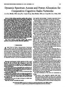
I. INTRODUCTION Modern technology scaling and integrating enable us to implement large bitwidth functional units (FUs) and registers. As a consequence, large-size data-flow intensive applications such as video processing become possible in a single die. With this benefit, there is a growing large gap in the difference of bits between the largest and the smallest data. It has been reported in [1] that full-sized registers are required for only about 15% of the generated data among SPEC 2000 benchmarks. In the traditional design assuming uniform bitwidths, it would make a large portion of resources redundant, resulting in circuit overhead (e.g., area and power). To overcome the problem, bitwidth-aware design has been studied in which the bitwidth of each resource is suitably optimized so as to minimize redundant bits. In the last decade, there have been several works studying bitwidth-aware circuits at the stage of high-level synthesis (HLS) (bitwidth-aware HLS) to have more chances of minimizing area of resources (e.g., [2], [3], and [4]). Since the area cost of resources is directly related to the bitwidth configuration, the objective becomes to minimize the total bitwidth for each resource. Figure 1(a) shows an example scheduling solution with the minimum latency, three control-steps (csteps), for a dataflow graph (DFG), wherein nodes represent operations (additions ‘+’ or multiplications ‘*’), and arcs represent data-dependences. The required minimum operation bitwidth is annotated beside each node. In the HLS assuming uniform bitwidths (traditional
Fig. 1. (a) An example operation scheduling solution. (b) and (c) are two bitwidth-aware register binding solutions, but (c) is better in terms of the if clock skew scheduling is allowed. minimum clock periods
HLS), this operation scheduling solution requires one 14x6-bit multiplier and two-bit adders (additions assigned to the same FU are colored in the same way). In bitwidth-aware HLS, on the other hand, it requires one 16-bit multiplier, one 12-bit adder, and one-bit adder. Therefore, we can reduce the cost for adders. This is an advantage of bitwidth-aware HLS. For another resource type, register, we can reasonably assume a linear relationship between area and bitwidth. In similar to FU, a major goal of register allocation and binding is to minimize the total bitwidths of registers. In [2], Cong et al. have proposed an integrated register allocation and binding algorithm for bitwidth-aware HLS, which can achieve a positive result. However, we will point out that it could become suboptimal if applying intentional clock skew to registers (clock skew scheduling (CSS) [5]) is allowed. Today, CSS is becoming a common technique for improving circuit performance in HLS (e.g., [6] and [7]). Figure 2 illustrates an example to explain how CSS works to reduce the clock period, where two FUs (delay information is the same as Fig. 1(a)) are connected in series with intermediate registers. In non-zero clock skew design, the minimum clock period (de) is dominated by the worst delay, then is noted as 13. However, inserting a delay of 3 into the clock input of the middle register, we can reduce to 10 since the slower FU can borrow timing slack from the faster FU.
Fig. 2. Clock period reduction by inserting a delay into the clock line.
In this paper, we first introduce CSS into bitwidth-aware HLS aimed at providing good properties to the clock skew exploration in the downstream design flow. Our goal is to develop an HLS design flow considering both bitwidth and CSS (Fig. 3). We take the first step toward tackling the problem of CSS during register allocation and binding for a given total bitwidths of registers. It is worth noting that there is one closelyrelated work. Huang et al. [6] have studied CSS problem in traditional HLS, with register binding. However, their approach cannot be directly applied to bitwidth-aware HLS due to the following reasons: (1) The register sharing possibility for bitwidth-aware HLS is different from traditional HLS due to the bitwidth constraint; (2) Huang’ approach assumes that the number of available registers is given as an input, but in bitwidth-aware HLS, the number of available bitwidths for registers is given instead. The number of available registers is not unique even for the same total bitwidths. Therefore, the contributions of this paper are as follows. • It discusses a new bitwidth-aware HLS design methodology, considering the useful clock skew (Section II); • It proposes a formal framework based on mixed integer linear programming (MILP) to exactly solve bitwidth aware register allocation, binding, and CSS simultaneously for minimizing the clock period (Section III); • It conducts experiments using the proposed MILP for several benchmark circuits, which confirms the effectiveness of our approach (Section IV). • In Section V, conclusion and future work are presented. II. BITWIDTH-AWARE HLS WITH CLOCK SKEW In this section, we will describe the proposed bitwidthaware HLS with clock skew, and formulate our problem. A. Bitwidth-Aware Register Allocation and Binding Bitwidth-aware register allocation is a process of deciding the number of registers and the bitwidth of each register. Bitwidth-aware register binding is a process of mapping data to registers so that the lifetime constraint is met, and a large-bit data is not assigned to a smaller-bit register [2]. In the following, we call them simply ‘register allocation’ and ‘register binding.’ Figure 1(b) shows register allocation and binding solutions for Fig. 1(a) obtained through Cong’ algorithm [2], where is the output data of , a rectangle represents the lifetime of a data with its bitwidth, is y- bit register, and for a set of data assigned to the same register, these lifetimes are drawn in the same column. These lifetimes are drawn in the same column. Maintaining the Integrity of the _
Fig. 3. Proposed desing flow for bitwidth-aware HLS with clock skew.
Specifications B. CSS Let denote the clock arrival time of register (referred to to as clock latency). For a datapath from register register , there are two types of clocking constraints: setup constraint and hold constraint. To prevent the data reaching a register too late relative to the following clock pulse, the clock skew must satisfy the following setup constraint: max , , where is the clock period, and , is the maximum-path delay from to . max To prevent the same clock pulse triggering the same data into two adjacent registers, the clock skew must satisfy the followmin , , ing hold constraint: where min , is the minimum-path delay from to . The set of timing constraints is modeled by an edgeweighted graph, called a constraint graph , where a set of vertices includes the vertices corresponding to registers, one special vertex, called the host , and a set of directed edges (arcs) with their weights is defined as follows: The setup constraint and the hold constraint: For each datapath from to , we add two arcs , and , to , associated with the weight of the righthand side of (1) and (2), respectively. The former and the latter arcs are referred to as S-arc and H-arc, respectively. The permissible range of clock latency: For each vertex , we add two arcs , and , to , associated with and , respectively, where is the weights / the maximum/minimum permissible clock latency. This type of arc is referred to as C-arc. From [8], we have the following lemma. conLemma 1: If and only if there is a CSS solution, tains no negative weighted cycle. If so, a CSS solution is ob. tained solving the shortest path problem from
•
Fig. 4. Constraint graph . (a) and (b) are respectively, where redundant arcs are removed.
for Figs. 1(a) and 1(b),
: A binary variable for each combination of data and register . If is assigned to , then the value of , is 1; otherwise, the value of , is 0. , which , : A real-valued variable for each represents the bitwidth of . ,
• •
Figure 4(a) shows for the register binding solution (Fig. 1(a)) under the assumption that the max/min-path delays of a multiplication are 13/4, the max-/min-path delays of an addition are 10/3, 10, and 0. The arc weight is annotated beside each arc, and an H-arc is drawn in a dash arrow. We know that cannot be reduced smaller than 13 due to the looped S-arc at vertex in , and 13 holds since there is no negative weighted cycle in that case. C. Motivation and Problem Formulation If applying CSS is allowed, different register binding solutions could lead to different . Figure 1(c) shows another register binding solution for the same register set with Fig. for Fig. 1(c). As we can see from 1(b). Figure 4(b) shows s, the arc set of could be changed by register these ) binding, thereby the relevant properties (i.e., CSS and could be also changed. In fact, solving the shortest path problem for Fig. 4(b), we know that 10. Register allocation is also important since the set of registers (i.e., the vertex set ) is determined by register allocation. This observation of during regmotivates us to optimize CSS for minimizing ister allocation and binding. The HLS problem to be solved in this paper, namely the bitwidth and clock skew-aware register allocation and binding problem is described as follows. Given: (1) An operation scheduled DFG; (2) FU allocation and binding results; (3) the maximum permissible clock latency range; (4) a bitwidth analysis result for data; (5) the number of available register bitwidths. Find bitwidth-aware register allocation, register binding, and CSS, such that the clock period is minimized. With respect to the computational complexity, we can prove that the problem is NP-hard based on a polynomial time reduction from an NP-complete problem the circular arc coloring problem [9] (details are omitted due to space limitations). Theorem 1: The bitwidth and clock skew-aware register allocation and binding problem is NP-hard. III. MILP-BASED APPROACH To exactly solve our optimization problem, in this section, we formulate the problem as an MILP. Although MILP is also NP-hard, it can be solved by an MILP solver (e.g., [10]). A. Variables Definition The variables used in our MILP are as follows:
: A real-value variable representing the clock latency of the register to which the output data of (i.e., ) is assigned. : A real-value variable representing the clock latency of .
•
B. MILP Constraints Since each data must be assigned to one register, we have the following constraint for each data : ∑ 1, (1) , where is a set of registers. Note that in bitwidth-aware HLS, the number of available registers could be changed even for the same total register bitwidths. Therefore, must be set as a large amount. If two data and have overlapping lifetimes, they cannot share the same register. Therefore, we have the following constraint for each register : 1. (2) , , in DFG, the setup and hold conFor each arc , straints can be written as follows: , (3) , (4) and are the maximum- and minimum where path delays to execute , respectively. (i.e., If and only if data is assigned to register 1), must be exactly the same as . For every , combination of and , we have the following constraints: 1
· 1 · (5) , is a constant value that approximates infinity. where To restrict the range of each clock latency, we have the following constraint for each register : ,
. (6) For every combination of and , if is assigned to , the bitwidth of must be smaller than : · , , (7) where is a constant representing the bitwidth of . Since the total bitwidths of registers must be no larger than the number of available register bitwidths (denoted as ), we have the following constraint: ∑ . (8) The objective is to minimize the clock period . Minimize : . (9)
C. Example We explain our MILP for the problem instance as shown in Fig. 1(a). Suppose that the number of registers | | is 3, and the number of available register bitwidths is 48. Due to the space limitation, we only show the MILP constraints (2) and (7) for data , and (8). Since is alive with at cstep 3, they cannot be assigned to a same register due to the lifetime 1, , constraint. Therefore, (2) becomes , , 1, and 1. If is assigned to , the bit, , , width of must be smaller than the bitwidth of . Therefore, , 14 · , , and 14 · , (7) becomes 14 · , . Finally, (8) becomes 48. IV. EXPERIMENTAL RESULTS We have carried out experiments on a set of HLS benchmark designs to evaluate the effectiveness of our synthesis flow in reducing the minimum clock period. Our synthesis flow has been implemented in C language, ran on a PC equipped with 2.40 GHz AMDR Dual OpteronTM. Each MILP was solved by CPLEXTM ver. 11.0.0 [10], on the same PC. We used two type FUs: ALU (addition/subtraction, max/min delay=10/3) and MUL (multiplication, max/min delay=13/4). We have used three benchmarks to evaluate the proposed approaches; namely, the 8-point fast Fourier transform (FFT8), the fifth-order elliptic wave digital filter (EWF), and the Fast Discrete Cosine Transform (FDCT). For the sake of simplicity, operation scheduling and FU binding were performed by non bitwidth-aware approach. , is set as 0, 10 . We evaluated the following three designs for comparison: • Only CSS: Register allocation and binding are obtained by Cong’ algorithm [2]. After that, CSS is optimized. • Our design: For the register bitwidths obtained by Cong’ algorithm, all of the register allocation and binding, and CSS are simultaneously optimized by our MILP. The latter parts of “Only CSS” can be formulated by our MILP with additional formulas, e.g., adding an equation 1 if data is assigned to register . We assigned a , value randomly to the bitwidth of each data, so that some bitwidth in between 8-bit and 16-bit is assigned to the output data of an addition, and some bitwidth in between 12-bit and 20-bit is assigned to the output data of a multiplication (our proposed design can also treat the practical data). Table I shows the result of minimum clock period comparison. In the column “time[s]”, the computation time, the time in parentheses means that the computation cannot terminate in one hour, but the temporal best solution (written in the column “ ”) was obtained in a time. For benchmarks 8-FFT and EWF, our proposed design could reduce the clock period compared to “Only CSS” design. For benchmark FDCT, our proposed MILP could not terminate and could not output temporal solution in one hour. Therefore, we fixed the register allocation (Cong’ algorithm solution), and ran our MILP. Then it terminated in a few second, but could not reduce the
clock period. It can be considered that exploring register allocation makes the solution space larger, and register allocation result affects the minimum clock period. V. CONCLUDING REMARKS For VLSI design in the nanometer regime, it is important to optimize bitwidth-aware circuits. In this paper, as one method to improve the performance of bitwidth-aware circuits, we have introduced the concept of clock skew scheduling into bitwidth-aware high-level synthesis, and presented a problem of minimizing the clock period during register allocation and binding. Our experiments using mixed integer linear programming showed that the proposed approach can reduce the minimum clock period by 9.4% on average, compared to conventional bitwidth-aware design without considering clock skew. To develop an efficient heuristic algorithm to obtain near-optimal solutions for large-size instances, and to deal with a variable path-delay depending on the bitwidth of functional units is left as a future work. REFERENCES [1] O. Ergin, D. Balkan, K. Ghose, and D. Ponomarev, “Register packing:Exploiting narrow-width operands for reducing register file pressure,” Proc, IEEE/ACM MICRO, pp. 304–315, Dec. 2004.
[2] J. Cong, Y. Fan, G. Han, Y. Lin, J. Xu, Z. Zhang, and X. Cheng, “Bitwidth-aware scheduling and binding in high-level synthesis,” Proc. IEEE/ACM ASP-DAC, pp. 856–861, Jan. 2005.
[3] N. Doi, T. Horiyama, M. Nakanishi, and S. Kimura, “Bit-length optimization method for high-level synthesis based on non-linear programming technique,” IEICE Trans. Fundamentals, vol. E89-A, issue 12, pp. 3427–3434, Dec. 2006.
[4] N. Chabini and W. Wolf, “Register binding guided by the size of variables,” Proc. IEEE ICCD, pp. 587–594, Oct. 2007.
[5] J.P. Fishburn, “Clock skew optimization,” IEEE Trans. on Computers, vol. 39, pp. 945–951, Jul. 1990.
[6] S.-H. Huang, C.-H. Cheng, Y.-T. Nieh, and W.-C. Yu, “Register binding for clock period minimization,” Proc. IEEE/ACM DAC, pp. 439–444, Jul. 2006.
[7] K. Inoue and M. Kaneko, “Early planning for RT-level delay insertion during clock skew-aware register binding,” Proc. IFIP/IEEE VLSI-SoC, pp. 154–159, Oct. 2011.
[8] T.H. Cormen, C.E. Leiserson, R.L. Rivest, and C. Stein, Introduction to Algorithms – Second Edition, The MIT Press, 2001.
[9] M. R. Garey, D. S. Johnson, G. L. Miller, and C. H. Papadimitriou, “The complexity of coloring circular arcs and chords,” SIAM Journal on Algebraic Discrete Methods, vol. 1, no. 2, pp. 216–227, 1980.
[10] IBM ILOG CPLEX, http://www.ilog.com