Boosting FM AX of Processor Pipelines using Intentional Memory Clock Skew Alexander Brant 1 , Ameer Abdelhadi 2 , Aaron Severance 3 , Guy G.F. Lemieux 4 Dept. of ECE, University of British Columbia Vancouver, Canada 2
[email protected]
3
Abstract—FPGAs are increasingly being used to implement many new applications, including pipelined processor designs. Designers often employ memories to communicate and pass data between these pipeline stages. However, one-cycle communication between sender and receiver is often required. To implement this read-immediately-after-write functionality, bypass registers are needed by most FPGA memory blocks. Read and write latencies to these memories and the bypass can limit clock frequencies, or require extra resources to further pipeline the bypass. Instead of further pipelining the bypass, this paper applies clock skew scheduling to memory write and read ports of a simple bypass circuit. We show that the clock skew provides an improved FM AX without requiring the area overhead of the pipelined bypass. Many configurations of pipelined memory systems are implemented, and their speed and area compared to our design. Memory clock skew scheduling yields the best FM AX of all techniques which preserve functionality, an improvement of 61% over the baseline clock speed, and consuming 50% fewer resources than the next best performing technique. Index Terms—design and applications; timing optimization; memory architectures;
I. I NTRODUCTION As FPGA capacities and speeds increase, they are being used for many new applications and architectures. These applications include high performance processing, which often employ custom pipelined circuits and accelerators, or general purpose processor pipelines [1][2]. Memories are often used to communicate and pass data between pipeline stages, to allow for more flexible computation. These memories may be located far away from computation resources such as DSPs on the FPGA, and the read and write latency to these memories can limit the resulting speed of processor circuits. These latencies can be reduced by pipelining the read and write ports, e.g. first writing data to higher speed registers that are written to memory in the next cycle. This approach will result in a communication latency between pipeline stages of a few clock cycles, which is undesirable and impractical for many architectures. By implementing bypass registers to hold and forward data written within the last one or two cycles, we can remove this limitation at the cost of resources and speed. In this paper, we pipeline a memory using clock skewing to effectively eliminate the read and write latency of the memories, while preserving functionality, and using fewer resources than conventional bypass designs. To allow communication
[email protected]
4
[email protected]
between pipeline stages without an extra cycle of latency, written data is written to a bypass register, and if the read address is the same as the write address from the previous cycle, the bypass register is selected instead of the memory output. By clocking the memory write ports slightly after the main clock, we can borrow time from the downstream logic stage to finish the data write (Fig. 1). In addition, in some situations, the read port can be clocked slightly before the main clock, reducing the time to read data. Extra resources on FPGAs such as multiple clock generators and global clock networks sometimes go unused by designers. Our design leverages these resources to improve the speed of pipelined circuits, and reduce usage of more general purpose resources such as logic and registers. Our memory design is applicable to many similar systems which use memories for communication, for example pipelines using FIFOs between compute elements, or two or more programmable CPUs which communicate through mailbox memories. While traditional skew scheduling technique introduces complex CAD techniques to solve a general optimization problem, our design isolates a specific frequent use-case that benefits from clock skew scheduling. The design can be integrated seamlessly by end users, and could be precompiled into an IP library that depends on properties of the device, not the end-user circuit.
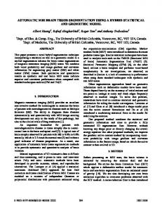
WR_data WR_addr WR_clk
X
RD_data RD_addr RD_clk
Ø-Δ2
WR_data WR_addr
Ø+Δ1
WR_clk
RAM
[email protected]
RAM
1
RD_data RD_addr RD_clk
Clock Period T
Ø Ø+Δ1 Ø-Δ2
Δ1
Δ2
Read to Write Clock Delay T+Δ1+Δ2
Fig. 1. Example of clock skew scheduling used to extend clock to clock delay for critical path
By combining memory bypassing and memory clock skewing, we can improve FM AX and reduce area usage over conventional pipeline bypassing, while maintaining function-
ality. We implemented other comparable memory designs, and compared them to our technique. Designs were evaluated using static timing analysis on an Altera Cyclone device. Overall, our pipeline memory design: • Improves FM AX by 56% over the baseline design, and 14% over the best conventional design. • Achieves the highest speed of any alternate design. • Consumes 50% fewer resources than the next-best performing design. II. BACKGROUND Clock skew scheduling, or clock skew optimization [3] is a time-borrowing technique used to increase the clock speed of circuits by allowing critical paths longer cycle times to propagate. By moving the clock transition from the source register of the critical path earlier than the transition of the sink, the critical path delay can be greater than the clock period without creating timing violations. The logic preceding and following the affected registers however will need to have sufficient slack to accommodate the skew, so if it is also on the critical path the technique will not be effective. Therefore the technique will be most effective in feed-forward pipelines. Fig. 1 shows how two oppositely skewed clocks can increase timing slack if used to register the source and sinks of a path. Useful clock skew can be applied to any design without user input, using natural skew inherent in any clock network. Some tools will automatically use clock skew to improve FM AX , e.g. skew scheduling is applied to FPGA CAD tools in [4] and [5], while a clock skew optimized FPGA architecture is explored in [6]. Clock skew scheduling is also used in pipelined designs and techniques such as ReCycle [7], where slower stages in a long pipeline receive slack from faster ones, bringing performance nearer to the average case delay of the pipeline, rather than the worst case. Pipeline bypassing, or forwarding [8], is a common technique in pipelined design where data is passed forward in a pipeline skipping over one or more register stages. When extra pipeline stages are introduced to increase circuit performance, forwarding can reduce the number of cycles of latency needed for an operation to complete, and increase overall performance. III. S KEWLESS D ESIGNS A. Baseline Design Our starter circuit in Fig. 1 is a simple feed-forward multistage pipeline of 8×8 bit multipliers, reading and writing 16 bits of data from simple dual-port block RAMs. The RAM write port is synchronous, latching the data, address, and writeenable on the write clock. The RAM read port captures the address synchronously on the read clock, and the read data comes out after the memory array is accessed. The memory write and read addresses come from separate registers not shown in the diagram. This design allows each pipeline stage single-cycle access to data in the memory. Since the block RAM and multiplier exist in separate parts of the FPGA, the FM AX can suffer from routing latency to and from memory, as well as the read and write delays to memory itself. According
to Quartus static timing analysis, this starter design operates at 126MHz in the Altera Cyclone IV FPGA of our Terasic DE2-115 board. In many FPGA memories, including those in Cyclone IV, data cannot be read on the same clock edge it is written. Instead, one additional cycle of latency must be introduced before the same address can be read between pipeline stages. This latency is undesirable for a processor design. To allow for data to propagate quickly between stages, the bypass circuitry shown in Fig. 2 is required. When ∆wr = ∆rd = 0, we call this the baseline design. The previously written data and address are saved in registers. An address comparator is employed to compare the last cycle’s write and current cycle’s read address. In the case of a match, a multiplexer feeding the Read Data line will switch to the register containing the last written data instead of the block RAM output. B. Memory with Fully Pipelined Bypass The circuit in Fig. 3 improves the FM AX performance of the baseline bypass circuit with additional pipelining. Both data and addresses for the previous two writes are stored in registers, and the read is initiated a cycle early. The addresses are compared, and the proper values from the memory or registers is selected. This increases the total resources used for each pipeline stage and memory, and introduces additional delay in the bypassing multiplexer. One drawback of this fully pipelined bypass is the additional LUT and FF resources required to implement two stages of bypassing. These resources could potentially be placed anywhere in the FPGA, increasing the uncertainty about wire propagation delays. The increased number of resources also increases the probability that the tools may produce a bad placement solution, potentially resulting in slower operation. IV. S TATIC C LOCK S KEW S CHEDULING In this section we present our design for a memory pipeline using clock skew scheduling. Our bypass design, shown in Fig. 2, employs a circuit similar to the original baseline design, except that some intentional clock skew ∆wr and ∆rd is being applied to the write and read ports of the memory, respectively. Note the write-data register is also clocked late by ∆wr , just like the memory write port. However, the writeaddress register is clocked normally or, if possible, clocked early by ∆rd . The bypass operates just like before. For correct readduring-write behaviour, the write address and write data are captured in registers. If the read address matches the write address from the previous cycle, the write-data register is selected by the bypass mux instead of the memory output. The presence of a bypass register allows us to borrow time by shifting both the read and write clocks without affecting functionality. The write port clock lags the main clock by ∆wr , borrowing time to allow the processing circuitry to finish and the data to be written. The read port leads the main clock by ∆rd , allowing the memory to be read in advance of when it will be needed.
bypass
1
wrAddr
Ø+Δ1
WR_data WR_addr WR_clk
RAM
wrData
rdData RD_data
0
rdAddr
RD_addr RD_clk
wrAddr
bypass
Ø+Δff
FF
X
WR_data WR_addr
Ø-Δ2
=
FF
rdAddr
Ø+Δwr
WR_clk
RAM
FF
RD_data RD_addr RD_clk
Ø+Δrd
FF Fig. 4.
Timing paths of memory
Fig. 2. Baseline memory circuit with single-stage bypass, also used for static clock skew scheduling when ∆wr ≥ 0, ∆rd ≥ 0
V. T IMING A NALYSIS Extra resources are available on FPGAs for multiple clock generators (eg, PLLs) and networks that often go unused. This design leverages these otherwise unused resources to improve the speed of pipelined circuits, and reduce usage of more general purpose resources such as logic and registers. While this new design also relies upon good placement of the bypass components, there are fewer resources to place than the twostage bypass circuit in Fig. 3. Time borrowing from the write operation of a preceding pipeline stage will only affect the next stage if the last-written data is needed immediately. In that case, since the value is always read from the bypass register, the time borrowed from the read and write ports will not cause latency to propagate into the next stage. Due to this condition, both the write and read ports of the memory can be skew scheduled to extend the time for the computation path. The values of ∆wr and ∆rd are mostly dependent on timing properties of the block RAMs. These can be precharacterized and precalculated, allowing the design of a clock-skewed memory with bypass to be an IP block. However, it is also possible to compute these timing properties at compile-time to automatically determine the skews.
bypass
FF
01
wrData
1Φ
rdData
The amount of clock skew applied to each memory port is derived from analyis of the timing paths through the circuit. There are four timing paths to consider between each memory stage (1) T ≥ ∆f f + tclk→out (ff) + td (ff→mux) + td (mux) + td (mul) + td (mul→ff) + tsu (ff) - ∆f f (2) T ≥ ∆f f + tclk→out (ff) + td (ff→mux) + td (mux) + td (mul) + td (mul→ramwr ) + tsu (ramwr ) - ∆wr (3) T ≥ ∆rd + tclk→out (ramrd ) + td (ramrd →mux) + td (mux) + td (mul) + td (mul→ff) + tsu (ff)-∆f f (4) T ≥ ∆rd + tclk→out (ramrd ) + td (ramrd →mux) + td (mux) + td (mul) + td (mul→ramwr ) + tsu (ramwr ) - ∆wr Timing path (1) is the limiting path, which can’t be improved by time borrowing since it from a flip-flop to a flip-flop with the same clock. Timing path (2) can be improved by time borrowing (∆wr ) and should have the same delay as path (1), hence: (5) ∆wr = td (mul→ramwr ) + tsu (ramwr ) - td (mul→ff) tsu (ff) + ∆f f Timing path (3) can be improved by time borrowing (∆rd ) and should have the same delay as path (1), hence: (6) ∆rd = tclk→out (ff) + td (ff→mux) - tclk→out (ramrd ) td (ramrd →mux) + ∆f f The delay of path (4) is achieved by applying (5) and (6) into path (4) as follows. (7) T ≥ ∆f f + tclk→out (ff) + td (ff→mux) + td (mux) + td (mul) + td (mul→ff) + tsu (ff) - ∆f f hence, similar path delay as path (1).
wrAddr
WR_addr WR_clk
wrAddr
FF Fig. 3.
RAM
VI. E XPERIMENTAL R ESULTS WR_data
RD_data
00
rdAddr
RD_addr RD_clk
= =
rdAddr
FF
Memory circuit with fully pipelined bypass
To evaluate the suggested time-borrowing method and to compare to the traditional bypass method, both methods have been implemented in Verilog and tested using Altera/Terasic DE2-115 board with a Cyclone IV E device (C7 speed grade). While static timing analysis (STA) is derived directly from Quartus II, a testing circuit is required as a proof-of-concept and to experimentally measure the performance limit of a real chip. Fig. 5 describes a performance testing circuit with a dualclocked RAM for tracing the DUT (design-under-test) results. The dual-clocked RAM is written by a DUT testing wrapper
Design Method Baseline design(Fig. 2), ∆wr = ∆rd = 0 Fully Pipelined Bypass (Fig. 3) Time-borrow (Fig. 2), Optimal ∆wr ,∆rd
FM AX (MHz) (QuartusII STA) 113 179 183 (∆wr = 2.0ns, ∆rd = 0ns)
FM AX (MHz) (Tested) 153 208 238 (∆wr = 2.0ns, ∆rd = 0ns)
#LUTs 21 37 21
#FFs 17 34 17
TABLE I FMAX AND R ESOURCE USAGE OF PIPELINE DESIGNS
!= error
Reset Generator Fig. 5.
Random
wrAddr
rdData
reset done?
wrData
Counter DUT
Tracing RAM
Counter done? reset
Low Freq. rdAddr
DUT
Random
High Freq.
Testing Circuit
at high frequency and read by a reference DUT wrapper at low frequency. Error is detected if reference wrapper output is different from the read memory data. In order to guarantee high performance, clock enables were avoided. When a full testing trace is finished, the system resets and starts a new testing loop. The DUT wrapper includes a random address generator and a one-pass LFSR counter to index the generated data. The RAM in the DUT is initialized with random values. The addresses are generated with a two-level LFSR counter. The two-level LFSR counter is an LFSR counter seeded with a different LFSR counter to guaranty highly random addresses. However, the test circuit is supposed to check read-after-write cases where the read and write addresses are the same. This happens rarely with totally random addresses, so we force the same address when a few specific LFSR bits show a specific bit pattern. To achieve maximum performance, the testing circuit and the DUT wrapper have been fully pipelined; however, pipeline stages are not shown in Fig. 5. Clock delay is implemented using two different methods as a proof-ofconcept. In the first method lcells are used to delay the clocks while in the second the PLL shifted clocks are used. While the lcells suffer from design and PVT variations, the PLL clocks are more stable. Table I lists the area and the performance of the suggested time-borrowing method and the traditional bypass approach for 16-bit data width and 8-bit address width. The suggested method uses 50% less registers and 43% less LUTs since the bypass method contains more address comparisons and wider muxes. While Quartus II STA shows only 3% performance improvement, the test circuit demonstrates a higher performance improvement of 14.4%. This high performance improvement is due to further tuning and delaying of the design clocks.
VII. C ONCLUSION This paper presented a way to use clock skewing to effectively eliminate the read and write latency of the block RAMs in a pipeline. We have increased FM AX and reduced area usage over conventional pipelined bypassing, while maintaining the same functionality. Although Quartus II conservatively estimates a maximum speed of 113MHz for a typical baseline bypassed memory, but we measured correct operation of a real chip at 238MHz using memory clock skewing. Our memory design is applied to pipelined processors that communicate through memories, but is applicable to many similar systems. While traditional clock skew scheduling techniques introduce complex CAD techniques to solve a general optimization problem, our design isolates a specific frequent use-case that benefits and is easy to solve. The design can be integrated seamlessly by end users, and could be precompiled into an IP library that depends only on properties of the device, not the end-user circuit. Although omitted for brevity, we also implemented other compatible memory designs by retiming, i.e. moving flip-flops forwards and backward. Using static timing analysis, we found that the clock skew technique presented here achieved the highest clock frequency over the other designs. The main drawback to this approach is the creation of shortpath or min-path problems. That is, because of the delayed write clock, it is possible to violate the hold condition if short paths exists through the combinational pipeline. Using ∆wr > 0 further increases the likelihood of these short paths becoming a problem. To work around this, all short paths need to be delay padded until they reach a total delay of ∆wr + ∆rd . R EFERENCES [1] J. Diaz, E. Ros, F. Pelayo, E. Ortigosa, and S. Mota, “FPGA-based realtime optical-flow system,” IEEE Transactions on Circuits and Systems for Video Technology, vol. 16, no. 2, pp. 274–279, Feb. 2006. [2] A. Hodjat and I. Verbauwhed, “A 21.54 Gbits/s fully pipelined AES processor on FPGA,” in Field-Programmable Custom Computing Machines, April 2004, pp. 308–309. [3] J. P. Fishburn, “Clock skew optimization,” IEEE Transactions on Computers, vol. 39, no. 7, pp. 945–951, July 1990. [4] X. Dong and G. Lemieux, “PGR period and glitch reduction via clock skew scheduling, delay padding, and GlitchLess,” in International Conference on Field-Programmable Technology, December 2009, pp. 88–95. [5] D. Singh and S. D. Brown, “Constrained clock shifting for field programmable gate arrays,” in ACM/SIGDA International Symposium on FPGAs, 2002, pp. 121–126. [6] C. Yeh and M. Marek-Sadowska, “Skew-programmable clock design for fpga and skew-aware placement,” in ACM/SIGDA International Symposium on FPGAs, 2005, pp. 33–40. [7] A. Tiwari, S. R. Sarangi, and J. Torrellas, “ReCycle: Pipeline adaptation to tolerate process variation,” in International Symposium on Computer Architecture, April 2007. [8] J. P. Hennessy and D. A. Patterson, Computer Architecture: A Quantitative Approach. Morgan-Kauffman, 1990.