FO4 delay of about 15ps, this translates to a bit period of about 165ps. A properly buffered wire could therefore support a throughput of about 6Gbps, a value 30 ...
Reliable high-throughput FPGA interconnect using source-synchronous surfing and wave pipelining by Paul Leonard Teehan B.A.Sc., The University of Waterloo, 2006 A THESIS SUBMITTED IN PARTIAL FULFILMENT OF THE REQUIREMENTS FOR THE DEGREE OF Master of Applied Science in The Faculty of Graduate Studies (Electrical and Computer Engineering) The University Of British Columbia (Vancouver) October, 2008 c Paul Leonard Teehan 2008
Abstract FPGA clock frequencies are slow enough that only a fraction of the interconnect’s bandwidth is used. By exploiting this bandwidth, the transfer of large amounts of data can be greatly accelerated. Alternatively, it may also be possible to save area on fixed-bandwidth links by using on-chip serial signalling. For datapath-intensive designs which operate on words instead of bits, this can reduce wiring congestion as well. This thesis proposes relatively simple circuit-level modifications to FPGA interconnect to enable high-bandwidth communication. High-level area estimates indicate a potential interconnect area savings of 10 to 60% when serial links are used. Two interconnect pipelining techniques, wave pipelining and surfing, are adapted to FPGAs and compared against each other and against regular FPGA interconnect in terms of throughput, reliability, area, power, and latency. Source-synchronous signalling is used to achieve high data rates with simple receiver design. Statistical models for high-frequency power supply noise are developed and used to estimate the probability of error of wave pipelined and surfing links as a function of link length and operating speed. Surfing is generally found to be more reliable and less sensitive to noise than wave pipelining. Simulation results in a 65nm process demonstrate a throughput of 3Gbps per wire across a 50-stage, 25mm link.
ii
Table of Contents Abstract . . . . . . . . . . . . . . . . . . . . . . . . . . . . . . . . . . . . . .
ii
Table of Contents . . . . . . . . . . . . . . . . . . . . . . . . . . . . . . . .
iii
List of Tables
. . . . . . . . . . . . . . . . . . . . . . . . . . . . . . . . . .
vii
List of Figures . . . . . . . . . . . . . . . . . . . . . . . . . . . . . . . . . .
viii
Acknowledgements . . . . . . . . . . . . . . . . . . . . . . . . . . . . . . .
xi
Dedication
xii
. . . . . . . . . . . . . . . . . . . . . . . . . . . . . . . . . . . .
1 Introduction
. . . . . . . . . . . . . . . . . . . . . . . . . . . . . . . . .
1
. . . . . . . . . . . . . . . . . . . . . . . . . . . . . . . .
1
1.1
Motivation
1.2
Research Questions
. . . . . . . . . . . . . . . . . . . . . . . . . . .
3
Design targets
. . . . . . . . . . . . . . . . . . . . . . . . . .
3
Overview of this work
. . . . . . . . . . . . . . . . . . . . . . . . . .
3
1.2.1 1.3
2 Background and Related Work 2.1
FPGAs 2.1.1
2.2
. . . . . . . . . . . . . . . . . . . . .
5
. . . . . . . . . . . . . . . . . . . . . . . . . . . . . . . . . .
5
Datapath FPGAs
. . . . . . . . . . . . . . . . . . . . . . . .
6
Pipelined interconnect . . . . . . . . . . . . . . . . . . . . . . . . . .
6
2.2.1
Register pipelining . . . . . . . . . . . . . . . . . . . . . . . .
8
2.2.2
Wave pipelining
. . . . . . . . . . . . . . . . . . . . . . . . .
8
2.2.3
Surfing
. . . . . . . . . . . . . . . . . . . . . . . . . . . . . .
10 iii
Table of Contents 2.3
Serial signalling schemes . . . . . . . . . . . . . . . . . . . . . . . . .
11
2.3.1
Asynchronous
11
2.3.2
Source-synchronous
2.3.3
Receiver-clocked systems
2.3.4
Data encoding
. . . . . . . . . . . . . . . . . . . . . . . . . . . . . . . . . . . . . . . . . . . . . . . . .
12
. . . . . . . . . . . . . . . . . . . .
12
. . . . . . . . . . . . . . . . . . . . . . . . . .
13
Timing uncertainty . . . . . . . . . . . . . . . . . . . . . . . . . . . .
15
2.4.1
Skew and jitter . . . . . . . . . . . . . . . . . . . . . . . . . .
15
2.4.2
Sources of timing uncertainty . . . . . . . . . . . . . . . . . .
17
2.4.3
Process corners . . . . . . . . . . . . . . . . . . . . . . . . . .
17
2.4.4
Statistical static timing analysis
. . . . . . . . . . . . . . . .
18
2.4.5
Statistical jitter modelling . . . . . . . . . . . . . . . . . . . .
19
2.4.6
Normal distributions . . . . . . . . . . . . . . . . . . . . . . .
19
Summary . . . . . . . . . . . . . . . . . . . . . . . . . . . . . . . . .
20
3 Design and Implementation . . . . . . . . . . . . . . . . . . . . . . . .
21
2.4
2.5
3.1
System-level design
. . . . . . . . . . . . . . . . . . . . . . . . . . .
21
3.2
Choice of serial signalling scheme . . . . . . . . . . . . . . . . . . . .
22
3.2.1
Global clock
. . . . . . . . . . . . . . . . . . . . . . . . . . .
23
3.2.2
Asynchronous
. . . . . . . . . . . . . . . . . . . . . . . . . .
24
3.2.3
Source-synchronous signalling . . . . . . . . . . . . . . . . . .
25
High-throughput pipelined circuit design . . . . . . . . . . . . . . . .
26
3.3.1
Rise time as a measure of throughput
. . . . . . . . . . . . .
26
3.3.2
Driving buffer strength
. . . . . . . . . . . . . . . . . . . . .
29
3.3.3
Multiplexor design . . . . . . . . . . . . . . . . . . . . . . . .
30
3.3.4
Wire length sensitivity . . . . . . . . . . . . . . . . . . . . . .
33
3.3.5
Wave-pipelining stage
. . . . . . . . . . . . . . . . . . . . . .
35
3.3.6
Surfing stage . . . . . . . . . . . . . . . . . . . . . . . . . . .
35
3.3
3.4
System-level area estimation
. . . . . . . . . . . . . . . . . . . . . .
36 iv
Table of Contents 3.5
Summary . . . . . . . . . . . . . . . . . . . . . . . . . . . . . . . . .
4 Robustness Analysis 4.1
. . . . . . . . . . . . . . . . . . . . . . . . . . . .
42
. . . . . . . . . . . . . . . . . . . . . . . . . .
42
4.1.1
Edge interference . . . . . . . . . . . . . . . . . . . . . . . . .
43
4.1.2
Incorrect sampling . . . . . . . . . . . . . . . . . . . . . . . .
47
4.1.3
Summary of criteria for reliable transmission
. . . . . . . . .
51
Quantifying timing uncertainty . . . . . . . . . . . . . . . . . . . . .
52
4.2.1
Process and temperature
. . . . . . . . . . . . . . . . . . . .
53
4.2.2
Crosstalk . . . . . . . . . . . . . . . . . . . . . . . . . . . . .
53
4.2.3
Supply noise model
. . . . . . . . . . . . . . . . . . . . . . .
56
4.2.4
Supply noise analysis
. . . . . . . . . . . . . . . . . . . . . .
58
4.3
Jitter and skew propagation . . . . . . . . . . . . . . . . . . . . . . .
60
4.4
Reliability estimate
. . . . . . . . . . . . . . . . . . . . . . . . . . .
63
4.5
Summary . . . . . . . . . . . . . . . . . . . . . . . . . . . . . . . . .
69
4.2
Reliable transmission
41
5 Simulation and Evaluation
. . . . . . . . . . . . . . . . . . . . . . . .
71
Throughput . . . . . . . . . . . . . . . . . . . . . . . . . . . . . . . .
71
5.1.1
Methodology . . . . . . . . . . . . . . . . . . . . . . . . . . .
71
5.1.2
Results
. . . . . . . . . . . . . . . . . . . . . . . . . . . . . .
73
5.1.3
Comparison . . . . . . . . . . . . . . . . . . . . . . . . . . . .
73
5.2
Latency . . . . . . . . . . . . . . . . . . . . . . . . . . . . . . . . . .
76
5.3
High-throughput wave pipelining . . . . . . . . . . . . . . . . . . . .
79
5.4
Area . . . . . . . . . . . . . . . . . . . . . . . . . . . . . . . . . . . .
80
5.5
Energy
. . . . . . . . . . . . . . . . . . . . . . . . . . . . . . . . . .
81
5.6
Summary . . . . . . . . . . . . . . . . . . . . . . . . . . . . . . . . .
83
6 Summary and Conclusion . . . . . . . . . . . . . . . . . . . . . . . . .
85
5.1
6.1
Summary . . . . . . . . . . . . . . . . . . . . . . . . . . . . . . . . .
85 v
Table of Contents 6.2
Interpretation of results . . . . . . . . . . . . . . . . . . . . . . . . .
88
6.3
Future work
89
. . . . . . . . . . . . . . . . . . . . . . . . . . . . . . .
6.3.1
Low-power design
6.3.2
Architectural exploration
6.3.3
Noise and reliability modelling
6.3.4
Silicon implementation
6.3.5
Wave-pipelined FIFO implementation
References
. . . . . . . . . . . . . . . . . . . . . . . . . . . . . . . . . . . . . . . . . . . .
89 89
. . . . . . . . . . . . . . . . .
90
. . . . . . . . . . . . . . . . . . . . .
90
. . . . . . . . . . . . .
90
. . . . . . . . . . . . . . . . . . . . . . . . . . . . . . . . . . . .
91
Appendices A Auxiliary Circuit Designs . . . . . . . . . . . . . . . . . . . . . . . . .
99
A.1 Serializer and Deserializer . . . . . . . . . . . . . . . . . . . . . . . .
99
A.2 Edge-to-pulse converter A.3 Delay element
. . . . . . . . . . . . . . . . . . . . . . . . . 101
. . . . . . . . . . . . . . . . . . . . . . . . . . . . . . 102
B Area Calculation Details
. . . . . . . . . . . . . . . . . . . . . . . . . 103
B.1 Area measurement methodology
. . . . . . . . . . . . . . . . . . . . 103
B.2 System-level area calculations . . . . . . . . . . . . . . . . . . . . . . 103 B.3 Block-level area tabulation
. . . . . . . . . . . . . . . . . . . . . . . 106
C Bounded Worst-Case Timing Uncertainty . . . . . . . . . . . . . . . 107
vi
List of Tables 2.1
Probabilities for standard normal distribution . . . . . . . . . . . . .
20
3.1
Approximate area cost of serializers, deserializers, and serial buses
.
38
5.1
Supply voltages used . . . . . . . . . . . . . . . . . . . . . . . . . . .
72
5.2
Area tabulation . . . . . . . . . . . . . . . . . . . . . . . . . . . . . .
81
5.3
Energy per transition measurements (fJ) . . . . . . . . . . . . . . . .
83
5.4
Energy estimates for 8b and 16b transfers . . . . . . . . . . . . . . .
83
B.1 Summary of area savings (min-transistors) . . . . . . . . . . . . . . . 104 B.2 Pre-serialization area . . . . . . . . . . . . . . . . . . . . . . . . . . . 104 B.3 Post-serialization area . . . . . . . . . . . . . . . . . . . . . . . . . . 105 B.4 Area tabulation . . . . . . . . . . . . . . . . . . . . . . . . . . . . . . 106
vii
List of Figures 1.1
Regular and serial programmable interconnect . . . . . . . . . . . . .
2
1.2
Increased throughput with pipelined interconnect . . . . . . . . . . .
2
2.1
Architectural drawing of an island-style FPGA . . . . . . . . . . . . .
7
2.2
FPGA switch block detail . . . . . . . . . . . . . . . . . . . . . . . .
8
2.3
Skew definition . . . . . . . . . . . . . . . . . . . . . . . . . . . . . .
16
2.4
Jitter definition . . . . . . . . . . . . . . . . . . . . . . . . . . . . . .
17
2.5
Illustration of process corners . . . . . . . . . . . . . . . . . . . . . .
18
3.1
Schematic of input and output connections, with existing parts in bold
22
3.2
High-level schematic showing interaction with user clock . . . . . . .
23
3.3
High-level timing diagram . . . . . . . . . . . . . . . . . . . . . . . .
25
3.4
Basic interconnect stage schematic . . . . . . . . . . . . . . . . . . .
26
3.5
Detail of 4-tile wire . . . . . . . . . . . . . . . . . . . . . . . . . . . .
27
3.6
RC wire model used in simulations . . . . . . . . . . . . . . . . . . .
27
3.7
Illustration of wide, minimum-width, and attenuated pulses . . . . . .
28
3.8
Driving buffer size analysis . . . . . . . . . . . . . . . . . . . . . . . .
31
3.9
Sixteen-input multiplexor schematic . . . . . . . . . . . . . . . . . . .
32
3.10 Rise time of muxes . . . . . . . . . . . . . . . . . . . . . . . . . . . .
32
3.11 Rise time of varying length wires . . . . . . . . . . . . . . . . . . . .
34
3.12 Wave pipeline interconnect stage . . . . . . . . . . . . . . . . . . . .
35
3.13 Surfing interconnect stage . . . . . . . . . . . . . . . . . . . . . . . .
37
viii
List of Figures 3.14 Surfing timing diagram . . . . . . . . . . . . . . . . . . . . . . . . . .
37
3.15 System-level interconnect area estimation . . . . . . . . . . . . . . . .
40
4.1
Waveforms showing pulse propagation through five stages . . . . . . .
44
4.2
Pulse width measurement circuit . . . . . . . . . . . . . . . . . . . .
45
4.3
Pulse transfer behaviour . . . . . . . . . . . . . . . . . . . . . . . . .
46
4.4
Pulse width transfer characteristic simulations . . . . . . . . . . . . .
48
4.5
Skew transfer measurement circuit
. . . . . . . . . . . . . . . . . . .
49
4.6
Skew transfer characteristic simulations . . . . . . . . . . . . . . . . .
50
4.7
Crosstalk simulation setup . . . . . . . . . . . . . . . . . . . . . . . .
55
4.8
Delay variation due to crosstalk . . . . . . . . . . . . . . . . . . . . .
56
4.9
VDD noise waveforms . . . . . . . . . . . . . . . . . . . . . . . . . . .
58
4.10 Experimental setup measuring delay impact of VDD noise . . . . . . .
59
4.11 Delay variation due to variations in DC level (σ = 15mV). . . . . . .
60
4.12 Delay variation due to transient supply noise (µ = 0.95V.) . . . . . .
61
4.13 Experimental setup measuring skew and jitter propagation . . . . . .
62
4.14 Jitter and skew propagation (simulation in bold) . . . . . . . . . . . .
63
4.15 Illustration of arrival time probabilities for consecutive edges . . . . .
64
4.16 Probability of error estimates . . . . . . . . . . . . . . . . . . . . . .
68
5.1
Throughput simulation results . . . . . . . . . . . . . . . . . . . . . .
74
5.2
Waveforms showing data at the end of a 50-stage link . . . . . . . . .
75
5.3
Waveforms showing stage-by-stage propagation
. . . . . . . . . . . .
76
5.4
Throughput comparison for all schemes . . . . . . . . . . . . . . . . .
77
5.5
Latency normalized to a regular wire, VDD µ = 0.95V, σ = 30mV . .
78
5.6
Latency with 400ps FIFOs at 5Gbps . . . . . . . . . . . . . . . . . .
80
A.1 Serializer (with clock generator) and deserializer circuits . . . . . . . 100 A.2 Serializer and deserializer timing diagrams . . . . . . . . . . . . . . . 101 ix
List of Figures A.3 Edge-to-pulse converter circuit . . . . . . . . . . . . . . . . . . . . . . 102 A.4 Delay element . . . . . . . . . . . . . . . . . . . . . . . . . . . . . . . 102 C.1 Comparison of normal and bounded models . . . . . . . . . . . . . . 108
x
Acknowledgements I would first like to thank my supervisors, Dr. Guy Lemieux and Dr. Mark Greenstreet, for their guidance, support, dedication, and patience. Each of them has taught me so much in such a short time. I would like to thank Dr. Jesus Calvino-Fraga for giving me an opportunity to teach; I will fondly recall my time in his superb introductory circuit lab courses. Also, I would like to thank Dr. David Pulfrey for his friendship and guidance. This work would not have been possible without the support of my friends and colleagues in the System on Chip lab at UBC. In particular, thank you to Daryl Van Vorst, Andrew Lam, Cindy Mark, David Grant, Rosemary Francis, Alastair Smith, Scott Chin, Marcel Gort, Darius Chiu, Faizal Karim, Mark Yamashita, and Roberto Rosales. Thank you finally to my parents for their unwavering love and support.
xi
To Shabnam, my favourite person in the world. Your love and encouragement has kept me going. Sorry to be cheesy, but I couldn’t have done it without you. This thesis is for you. 1Gbps) links [50]. Gaussian distributions are usually used to model random jitter [51]. Statistical jitter models do not appear to have been applied to on-chip interconnects before; this thesis will demonstrate that they are required for wave pipelined links.
2.4.6
Normal distributions
A good deal of the work in this thesis will assume that random effects are normally distributed. This assumption can be justified by the central limit theorem, which states that the sum of a sufficiently large number of random variables with finite mean and variance tends to be normally distributed. For example, since noise effects tend to be caused by the aggregation of many small random effects, the overall noise will tend to be normal. This is not a perfect assumption; its limitations will be highlighted later when it is applied. Random variables are characterized by their mean µ, and standard deviation, σ (or the variance, σ 2 ). A normally distributed random variable X with mean µ and standard deviation σ is notated as X ∼ N (µ, σ 2 ). Improbable events are often described in terms of the number of standard deviations away from the mean which corresponds to the event’s probability. For example, about 95% of all events occur 19
Chapter 2. Background and Related Work within two standard deviations of the mean, so a 2σ event occurs with about 5% probability. Table 2.1 lists the probabilities of such events up to ten standard deviations from the mean. In the table, P (|X ∼ N (0, 1)| > n) represents the probability that a random variable X which is normally distributed with mean µ = 0 and standard deviation σ = 1 takes a value greater than ±n. Since the standard deviation of X is 1, n is equal to the number of standard deviations away from the mean. Table 2.1: Probabilities for standard normal distribution n P (|X ∼ N (0, 1)| > n) 1 0.32 2 0.046 3 2.7×10⁻³ 4 6.3×10⁻⁵ 5 5.7×10⁻⁷ 6 1.9×10⁻⁹ 7 2.6×10⁻¹² 8 1.2×10⁻¹⁵ 9 2.3×10⁻¹⁹ 10 1.5×10⁻²³
2.5
Summary
This work applies wave pipelining and surfing to datapath FPGA architectures using source-synchronous signalling. It is not the first study of source-synchronous wavepipelined interconnect in FPGAs, but it is the first to consider surfing for the same application, and the first to consider reliability. The reliability analysis models jitter and skew using statistical methods which do not appear to have been previously applied to on-chip links.
20
Chapter 3 Design and Implementation This chapter describes an FPGA with high-bandwidth, bit-serial interconnect at the system and circuit levels. In the circuit-level description, circuit and timing diagrams are presented. The wave-pipelined and surfing interconnect circuits that will be analyzed later in this thesis are introduced here. Finally, a high-level area estimation is performed to predict the advantages of switching from parallel to serial interconnect.
3.1
System-level design
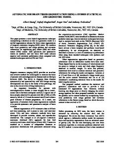
To efficiently support serial interconnect, the traditional FPGA architecture must be altered. Serializer (SER) and deserializer (DES) blocks must be added to each logic, memory, and multiplier block that supports serial communication. Additional switches to connect the SER and DES blocks to the regular block inputs and outputs are required as well. Finally, the wires must be optimized at the circuit level to maximize speed and reliability. Figure 3.1 shows a high-level architectural drawing of an FPGA with the existing parts in bold. The figure includes dedicated clock lines and a clock generator which is necessary to implement a source-synchronous signalling scheme; this particular choice of signalling is addressed in Section 3.2 Figure 3.2 shows a high-level circuit schematic serial interconnect. Note how the user clock controls a serial clock generator at the data source; this serial clock is sent alongside the data and is used at the receiver to clock the deserializer. Circuit diagrams for the serializer and deserializer circuits are provided in Appendix A. The 21
Chapter 3. Design and Implementation CLB / Memory / Multiplier
CLB / Memory / Multiplier
Block outputs
Output switches
Single wires
Serial buses
SER 11 00 00 11 00 11 00 11 00 11 00 11 00 11 00 11 00 11 00 11 Clk gen 00 11 00 11 00 11 00 11 00 11 00 11 SER 00 11 User clock 00 11 00 11 00 11 00 11 00 11 00 11 00 11 00 11 00 11 00 11 00 11 11111111111 00000000000 00 11 00 11 00 11 00 11 11111111111 00000000000 00 11 00 11 00 11 00 11 00 11 00 11 00 11 00 11 11111111111 00000000000 00 11 00 11 00 11 00 11 11111111111 00000000000 00 11 00 11 00 11 00 11 Programmable 11111111111 00000000000 00 11 1 0 11111111111 00000000000 Interconnect 00 11 11111111111 00000000000 1 0 11111111111 00000000000 00 11 1 0 11111111111 00000000000 00 11 data clk data
clk
Block inputs
11 00 00 11 00 11 00 11 00 11 00 11 00 11 00 11 00 11 00 11 00 11 00 11 00 11 00 11 00 11 00 11 DES 00 11 00 11 00 11 00 11 00 11 00 11 00 11 0 1 00 11 0 1 00 11 00 11 00 11 00 11 11111111111 00000000000 00 11 00 11 00 11 00 11 0 1 00 11 00 11 00 11 00 11 11111111111 00000000000 00 11 00 11 00 11 00 11 00 11 00 11 00 11 00 11 11111111111 00000000000 0 1 00 11 00 11 00 11 00 11 00 11 00 11 00 11 00 11 11111111111 00000000000 0 1 00 11 00 11 00 11 00 11 0 1 0 1 11111111111 00000000000 00 1 00 11 1 11111111111 00000000000 0 1 00 11 0 1 11111111111 00000000000 1 1 0 0 11111111111 00000000000 00 11 1 0 11111111111 00000000000 0 1 00 11 0 1 0 1 0 1 DES
Input switches
Figure 3.1: Schematic of input and output connections, with existing parts in bold
detailed design of the interconnect segments is described in Section 3.3.
3.2
Choice of serial signalling scheme
The serial data needs to operate at a rate much faster than the regular user clock; an FPGA with serial interconnect will therefore require a way of transmitting and recovering serial data that does not rely on the user clock. Possible techniques for doing so were reviewed in Section 2.3; they include using a high-speed global clock, asynchronous signalling, and source-synchronous signalling. Source-synchronous signalling is chosen because it is likely to require less power than a global clock, and because it is easier to integrate into a typical FPGA than asynchronous signalling. This rationale is elaborated below.
22
Chapter 3. Design and Implementation Destination registers
Source registers
DQ
DQ
DQ
DQ
Local logic and routing
Local logic and routing
DQ
DQ
DQ
DQ
Pipelined high−throughput programmable interconnect Serial data SER
DES Serial clock
Serial clock generator
Programmable delay
User clock (global)
Figure 3.2: High-level schematic showing interaction with user clock
3.2.1
Global clock
The most straightforward way of controlling the SER and DES blocks is with a highspeed global clock that is distributed throughout the chip. This scheme needs just one wire to send data using either wave pipelining or register pipelining. Data validity can be established with a pilot bit. To reach the 6Gbps target rates in this thesis, a low-skew double data rate clock in the 3GHz range is required. Designing clock networks at this speed is challenging, but has been done microprocessors. For example, the IBM Power6 can be clocked as high as 5Ghz, and uses less than 100 W for power-sensitive applications [52]. At 22% of the total power consumption, clock switching is a primary component [53]. Clock power is often controlled by disabling or gating the clock when it is not needed, but this is unlikely to save significant power in this situation. The global clock is needed to control serializers, deserializers, and interconnect pipeline latches. 23
Chapter 3. Design and Implementation Serial interconnect circuits that are not needed could be statically disabled using SRAM configuration bits. However, since clock gating is likely to be implemented at the tile level, any tile which contains active interconnect pipeline latches would not be able to disable the global clock. It would thus be difficult to realize appreciable power savings with clock gating. Source-synchronous is more attractive than global clocks from a power perspective; in the former case, the dynamic power is directly proportional to the number of serial bits transmitted, rather than a large fixed cost as in the latter case.
3.2.2
Asynchronous
Asynchronous schemes are attractive because they can tolerate an unbounded amount of timing uncertainty by using request/acknowledge handshakes instead of relying on signals to arrive within a certain time window. However, in FPGAs, links must be programmable, which requires that the req/ack handshake signals travel over a programmable path. Regular FPGA interconnect is not intended to route asynchronous handshakes. In a two-wire handshake, the acknowledgement must be reverse-routed back to the source, which adds some delay and power overhead. Supporting fanout is a bit more complex: after a request at the splitting point, the sender needs to wait for all receivers to acknowledge before sending the next token. One-wire or bidirectional-wire handshake schemes also exist [30] and have been recently adapted for serial signalling in a network-on-chip [54]. In such schemes, the request resets one end of a shared wire and the acknowledge sets the other end of the wire in response. Implementing this on an FPGA requires bidirectional transmission through the interconnect switches. This would negate the strong advantages of directional, single-driver wiring [55]. In general, source-synchronous signalling seems to be more easily adaptable to typical FPGA programmable interconnect than asynchronous signalling. 24
Chapter 3. Design and Implementation
3.2.3
Source-synchronous signalling
In a source-synchronous link, the timing reference is generated at the data source and is transmitted along with the data. A high-level timing diagram showing an 8-bit source-synchronous serial transfer is shown in Figure 3.3, in which the clock is sent on a separate wire, and data is sent on both edges of the clock. User clock Serial clock Serial data
Figure 3.3: High-level timing diagram
Off-chip serial links often use source-synchronous signalling, but rather than use an extra wire for the clock as in the figure, the timing information is typically embedded into the data signal using specialized encodings. The receiver then recovers the clock from the data using a clock-data recovery (CDR) circuit. This technique is not of interest here for three main reasons: 1. It relies on analog signalling techniques which are not compatible with typical FPGA multiplexors. 2. The transmitter and receiver are relatively complex to design and have high overhead in order to handle the various signal integrity issues in off-chip links, but on-chip links are not nearly as challenged by signal integrity. 3. CDR’s typically use phase-locked-loops, which work well for streams, but not bursts, because they take a relatively long time to lock (for example, 60ns in [56]). Sending the clock on a second wire is a much simpler technique. There is extra area overhead for the wire and power overhead for the extra timing transitions, but 25
Chapter 3. Design and Implementation this is largely unavoidable. An advantage of clock forwarding over using a global clock is that with clock forwarding, the power overhead is proportional to the number of bits transferred which allows the designer to trade off the amount of serial communication against power consumption.
3.3
High-throughput pipelined circuit design
This section describes the design of the multiplexor and drivers which are included in each interconnect stage, with throughput as a primary design goal. Figure 3.4 shows the schematic of each interconnect stage. The first driver is assumed to be twice minimum size, while the last driver is variable and will be determined in this section. The middle driver size is chosen so that each driver has equivalent effort [45]. The 0.5mm wire spans four tiles and includes mux taps after each 0.125mm tile as shown in Figure 3.5. In simulations, each 0.125mm wire is modelled with the 4-segment π-model shown in Figure 3.6, which is sufficiently accurate for this application [45]. 0.5mm 4−tile wire in
out 2x
2W
W
16:1 mux
Figure 3.4: Basic interconnect stage schematic
3.3.1
Rise time as a measure of throughput
In a throughput-centric design, the maximum bandwidth of the link is the inverse of the minimum pulse width that can be transmitted. An analytical throughput model is developed in [57] for a wave-pipelined link. Although the model is designed for inverter-repeated links only (to remain accurate, it would have to be modified to
26
Chapter 3. Design and Implementation Possible outputs
Driving buffer 0.125mm
0.125mm
0.125mm
0.125mm
Nominal output 16:1 muxes
0.5mm wire
Possible outputs
Figure 3.5: Detail of 4-tile wire R/4
R/4
R/4
R/4
in
out C/8
C/4
C/4
C/4
C/8
Figure 3.6: RC wire model used in simulations
include the effect of the multiplexors in an FPGA), a detailed analytical model is not necessary for first-order estimates. In the same study, rise time was shown to be a reasonably good approximation of throughput. To illustrate how rise time approximates throughput, consider the three pulses shown in Figure 3.7; assume these are waveforms at the output of a gate in the signal path which has a constant edge rate. A pulse is composed of a rising edge followed immediately by a falling edge (or vice versa); since each edge represents a data symbol, the pulse is formed by two consecutive symbols. The wide pulse saturates at the rail for some length of time; it could be made narrower with no ill effects. The minimumwidth pulse just barely reaches the supply rail; it is the narrowest pulse that can be transmitted through this gate without intersymbol interference. The attenuated pulse does not reach the supply rail because the edges are too close together in time. This pulse will likely be further attenuated by subsequent gates in the signal path
27
Chapter 3. Design and Implementation Voltage
Voltage
90%
90%
50%
50%
10%
10%
Voltage 90% 50%
10% Time
Time
pw trise
(a) Wide
pw trise
(b) Minimum width
Time pw
(c) Attenuated
Figure 3.7: Illustration of wide, minimum-width, and attenuated pulses
and eventually dropped. The rise time, measured from 10% to 90% of the swing, is trise and the pulse width, measured from 50% of the rising edge to 50% of the falling edge, is pw. Considering the minimum-width pulse and looking at only the rising edge, notice that the time from when the signal crosses the 50% threshold to the time when it reaches the rail is equal to pw/2. Because we assume the edge is perfectly linear, then the time from when the signal starts at 0% to when it reaches the 50% threshold is also pw/2. In other words, the 0% to 100% rise time is equivalent to the minimum pulse width. If rise time is measured from 10% to 90%, as in trise , then pw = trise /0.8. Realistic pulses are not perfectly linear, especially as the approach the rails, but this first order approximation is useful in the design process undertaken in subsequent sections. From this observation, it follows that fast edges are required to achieve a high bandwidth link. Hence, all gates must be properly sized relative to the loads they drive. An underpowered gate will produce slow edges which will limit the achievable bit rate. Of course, larger gates require more area and power, so size must be kept as low as possible while still meeting throughput targets.
28
Chapter 3. Design and Implementation
3.3.2
Driving buffer strength
Since the final driver must drive a 0.5mm wire with mux loads as shown in Figure 3.5, a series of simulations were run to determine how large this driver should be, relative to a minimum-sized inverter. Area, delay, energy, and rise time were measured; areaenergy-delay product and area-energy-delay-rise time product were calculated from the measurements. The methodology is briefly described below. • Area: sum of the area of a multiplexor and three inverters, sized as shown in Figure 3.4. Area is measured in minimum-transistor widths according to the methodology described in Appendix B. • Delay: average latency through a stage, including a 16:1 multiplexor, three tapered inverters, and a wire segment. • Energy: measured by integrating the charge drawn from the supply, multiplying by the supply voltage, and dividing by the number of edges. • Rise time: Measured at wire output (at the input of the next multiplexor3 ) from 10%VDD to 90%VDD . Simulations were conducted at the TT corner at room temperature. Results are shown graphically in Figure 3.8. As expected, area and energy grow with buffer size. Delay is optimal at about 35X, and rise time is optimal for very large buffers. Area-energy-delay product is a cost function that might be used for a typical FPGA wire design which does not explicitly require fast edges. The optimal buffer size in this case is about 15X. However, a 15X buffer is undersized relative to the wire load and produces a slow rise time. The area-energy-delay-rise time product suggests that 30X is the optimal size, but the 3
The measurement is taken here rather than at the multiplexor output so as to make the measurement dependant only on the inverter sizing, not the multiplexor design.
29
Chapter 3. Design and Implementation curve is relatively flat in the 25X to 40X region indicating that any size within this region is close to the optimal. To save area and energy, the final driver size will be fixed at 25X for this thesis.
3.3.3
Multiplexor design
Each interconnect segment includes a 16:1 multiplexor. The architecture is a 2-level hybrid design described in [58, 59] and shown in Figure 3.9. While FPGAs sometimes use NMOS-only multiplexors [58], in this case full CMOS transmission gates are required to improve edge rates and signal swing. Adding the PMOS transistor incurs a significant area penalty as twenty PMOS transistors are required in total. The width of these transistors must be kept as small as possible to save area. The output rise time of the multiplexor was measured from 65nm HSPICE simulations using transmission gates of specific sizes. Figure 3.10 shows the results. The x-axis shows the transistor sizes as multiples of a minimum-width NMOS transistor; for example, a 1x2-sized transmission gate contains minimum-width NMOS and twice-minimum width PMOS transistors. Output rise time is plotted; the data points represent measurements at the TT corner with a 1.0V supply, while the error bars show measurements at the SS corner with an 0.8V supply and the FF corner with a 1.2V supply. Both rising and falling edges are shown. There is not much advantage to increasing the width of the transistors. Rise time decreases slightly with wider transistors, but the magnitude of the decrease is minimal and it is clearly not worth the extra area. This result occurs because the decrease in resistance due to wider transmission gates is accompanied by an increase in diffusion capacitance; the added penalty offsets the gains. Not surprisingly, having an undersized PMOS, such as the 1x1 case, causes slow rising edges. In the SS corner, a rising edge has a rise time of 130ps while a falling edge has a rise time of 70ps. In the 1x2 case, where the PMOS is properly sized to be 30
Chapter 3. Design and Implementation
Delay 150
190
145 Avg stage latency (ps)
Area (Min transistor widths)
Area of stage (mux+all drivers) 200
180 170 160 150 140 130
140 135 130 125 120 115
120 10
20 30 40 Final driver size (min−inv widths)
110 10
50
20 30 40 Final driver size (min−inv widths)
(a) Area
−14
x 10
(b) Delay
Energy
Rise time 180
9.5
160
9
140
Rise time (ps)
Avg energy (joules per bit per stage)
10
8.5 8 7.5
120 100 80
7 10
20 30 40 Final driver size (min−inv widths)
60 10
50
20 30 40 Final driver size (min−inv widths)
(c) Energy
−21
x 10
Area−energy−delay
−19
2.5
1.8
1.6
1.4
1.2
1 10
20 30 40 Final driver size (min−inv widths)
(e) Area-Energy-Delay product
50
(d) Rise time
Area−energy−delay−risetime product
Area−energy−delay product
2
50
50
x 10
Area−energy−delay−risetime
2
1.5
1 10
20 30 40 Final driver size (min−inv widths)
50
(f) Area-Energy-Delay-Rise time product
Figure 3.8: Driving buffer size analysis
31
Chapter 3. Design and Implementation in1
in2
in3
in4 out r1F
in5
in6
in7
in8
r1T r2F
in9
in10
in11
in12
r2T r3F
in13
in14
in15
in16
r3T r4F
r4T c1T
c1F
c2T c2F
c3T
c3F
c4T
c4F
Figure 3.9: Sixteen-input multiplexor schematic Rise time at multiplexor output 140 Rising edge Falling edge 120
Rise time(ps)
100
80
60
40
20
1x1 1x2 2x2 2x4 3x6 Transmission gate size (NMOSxPMOS)
Figure 3.10: Rise time of muxes; error bars show process variation
twice as wide as the NMOS, the rising edge takes 110ps while the falling edge takes 90ps. The latter of the two is preferable since it leads to more consistent behavior, which is especially important for propagating timing edges. Thus, the muxes in this design will use 1x2-sized transmission gates. The simulations indicate a rise time of about 110ps in the worst case; since this is the 10% to 90% rise time, the actual minimum pulse width that the mux can
32
Chapter 3. Design and Implementation propagate is about 110ps/0.8≈140ps. This first-order estimate is relatively close to the 11 FO4-delay limit for ISI [3] of 165ps in this process.
3.3.4
Wire length sensitivity
It has been assumed that each interconnect stage includes a 0.5mm wire split into four segments, with multiplexors between each segment. It is useful to determine if the results in this thesis are sensitive to changes in wire length in case the results are applied to an architecture with different tile dimensions. Assume the driving buffer has a resistance of Rg and a diffusion capacitance of Cd ; assume the wire has a resistance of Rw and a capacitance of Cw ; and assume any additional load is Cl . From [60], the delay of a wire is as follows: 1 Delay ∝ Rg (Cd + Cw + Cl ) + Rw ( Cw + Cl ) 2
(3.1)
To improve the bandwidth, we must decrease the delay. Increasing the size of the driver, and thus decreasing Rg , will decrease the first term in equation 3.1, but not the second; the latter term is fixed for a given wire. If the wire is sufficiently short, such that Rw and Cw are small, then increasing the driver size will improve the bandwidth. If the wire is too long, increasing the driver will have little effect. Figure 3.11 shows the rise time at the end of wires of various lengths, under slow, typical, and fast conditions. At the nominal wire length of 0.5mm, the final driver is 25X minimum-sized. The size of the driver is scaled linearly with the wire, such that a 1mm wire has a 50X driver, and so on. The graph suggests that wires of length 1mm or more in this particular technology are too long to maintain fast edge rates. Such wires could be simply split into segments 0.5mm long with a 25X driver at each segment. Wires of 0.5mm or less are not wirelimited; since the driver is scaled linearly with the wire, they all achieve similar
33
Chapter 3. Design and Implementation Rise time of buffered wires 400 350
Rise time (ps)
300 250 200 150 100 SS/0.8V TT/1.0V FF/1.2V
50 0 0
0.5
1 Wire length (mm)
1.5
2
Figure 3.11: Rise time of varying length wires
bandwidth. Wires in this range could thus achieve higher bandwidth by increasing the driver size. It should also be considered that the worst-case multiplexor rise times are about 110ps. There is no benefit to improving wire rise times below this since the overall system bandwidth is constrained by the multiplexor. In fact, since larger drivers carry area and energy penalties, the drivers should be sized as small as possible so long as the wire edge rate is faster than the mux edge rate. The chosen design point of 25X is reasonably close to that point. To support high-rate serial transfers, both wave pipelining and surfing require some further modifications to the interconnect circuits. The wave-pipelined circuit needs two regular wires placed side by side with transistor sizes optimized for fast edge rates; the surfing circuit is somewhat more complex. One stage for each scheme is described below in more detail. Later in this thesis, multi-stage links will be discussed; these consist of a series of identical interconnect stages like the ones in this section cascaded together. The performance of the overall link is determined by the performance of one such stage, so proper design is very important.
34
Chapter 3. Design and Implementation
3.3.5
Wave-pipelining stage
The wave-pipelined link requires that the corresponding data and timing signal be routed side-by-side to eliminate skew. If we assume the wires are reserved for serial interconnect only, then the multiplexors for the data and timing wires may share one set of configuration bits since they follow the same route. Figure 3.12 shows the circuit diagram for a wave-pipelined interconnect stage with one data wire. Additional data wires may be added as needed. Transistors must be carefully sized to maximize throughput. 0.5mm 4−tile wire Data in
Data out 2x
7x
25x 0.5mm 4−tile wire
Clk in
Clk out 2x
7x
25x
16:1 muxes
Figure 3.12: Wave pipeline interconnect stage
Notice that the circuits are open-loop; jitter and skew can accumulate through many cascaded stages. Surfing interconnect, as described in the next section, may be used to attenuate both jitter and skew.
3.3.6
Surfing stage
The circuit structure of surfing [23, 24], shown in Figure 3.13, is similar to wave pipelining, with two key additions: 1. the clock line has a variable strength buffer which is controlled by a delayed version of the clock, and 2. the data line has a variable strength buffer which is controlled by the clock.
35
Chapter 3. Design and Implementation The variable-strength buffers are composed of a weak inverter in parallel with a strong tri-state inverter. The tri-state inverter is off until its control signal arrives. With proper design, the data or clock edge should arrive at the variable-strength buffer slightly ahead of the control signal, so that its transition is weak for some amount of time, then strong as the tri-state inverter turns on. In this case, if the edge arrives too early, a longer period of time passes before the tri-state inverter turns on, which means the edge has been slowed down. Likewise, if the edge arrives late, the tri-state inverter will turn on earlier (or may already be on), so the output transition is stronger and the late edge has been sped up. This means that edges are attracted to their control signals. Figure 3.14 illustrates timing with surfing. By configuring the clock line to be controlled with an echo of itself, and by setting the delay equal to the nominal clock half-cycle period, the surfing buffer implements a simple delay-locked loop [25]. Likewise, by controlling the data line with the clock, the surfing buffer acts similar to a pulsed latch. The clock edges are converted to pulses using a simple edge-to-pulse converter circuit.4 The two surfing buffers can thus remove jitter on the timing line and skew between the data and timing lines. Circuitlevel details of the delay element and edge-to-pulse circuit are given in Appendix A.
3.4
System-level area estimation
To estimate the possible area savings of a serially-interconnected FPGA, two new architectural parameters are required: M , the serial bus width, and Ps , the percentage of original wiring resources which are now replaced with serial buses. For example, in an FPGA with Ps = 0.25, M = 8, and a channel width W =64, there will be 48 regular wires and 2 serial buses carrying 8 bits of data each; a total of 16 wires or 4
Data edges tend to lag a small amount behind timing edges due to the latency of the edge-topulse converter. The timing path must be slower than the data path in strong mode, but faster than the data path in weak mode. This allows the data signal to keep up with the timing signal. Hence, a few extra inverters are added to the timing path.
36
Chapter 3. Design and Implementation
1x
5x
d1
Data in
0.5mm 4−tile wire
d2
Data out
2x
25x
16:1 mux en
en edge to pulse
1x
5x
2x
2x
0.5mm 4−tile wire
surf_out
surf_in
Clk in
Clk out 25x
2x
16:1 mux surf_en
delay
Figure 3.13: Surfing interconnect stage
Timing buffer strength
weak strong
weak strong
weak strong
Surf_in
Surf_en
Surf_out
en en Data buffer strength
weak
strong
weak
strong
weak
d1
d2
Clk out
Data out
Figure 3.14: Surfing timing diagram
37
Chapter 3. Design and Implementation
Serializer Deserializer Single wire Serial bus
Base transistor cost 138 160 152 272
Transistors per bit 54 54 – 131/8
Total for M=8 570 592 – 403
Table 3.1: Approximate area cost of serializers, deserializers, and serial buses
25% of the channel were replaced by serial resources. Approximate area costs for serializers, deserializers, and interconnect is shown in Table 3.1. This data is based on the circuits described earlier and in Appendix A, and on area details shown in Appendix B. Wire area includes multiplexors, buffers, and other logic. Here, each serial bus contains one timing wire and one data wire. The following assumptions will be made when designing an FPGA with serial interconnect: • The target FPGA is island-style with 512 channel wires5 , all of length 4, and input connectivity of fc = 0.2. Each block has 64 inputs6 and 32 outputs. One quarter of the channel wires are available to be driven from each block. • One serial bus of width M can replace M single wires with no impact on routability. • Each block must contain enough M -bit deserializers such that 100% of block inputs can be supplied from serial buses. Likewise, each block must contain enough M -bit serializers such that 100% of block outputs can be sent over serial buses. These assumptions can be used to estimate area for a range of different architectures. While the precise architectural results will depend on proper benchmarking 5
This represents the sum of both horizontal and vertical channels. The block was assumed to be a DSP/multiplier, which needs more SER and DES blocks than a typical CLB. 6
38
Chapter 3. Design and Implementation and evaluation, we can gain insight into sensitivity of results here without benchmarking. Total interconnect area in a block can be measured by tabulating input connection mux area, wire mux and buffer area, and SER/DES overhead area. The target FPGA initially has a total interconnect area, including all input muxes, output muxes, and output buffers, of about 31616 minimum-transistor-widths per block. Roughly half of this comes from the input muxes: each of the 64 inputs is driven by a 77-input mux. The other half comes from the 16:1 muxes and buffers attached to each output wire. By converting a certain percentage of the 512 wires to serial buses, the input mux widths are reduced, and many of the output muxes and buffers can be removed. The three graphs in Figure 3.15 shows how the interconnect area varies with Ps , the percentage of wires that are converted to serial buses, and M , the serial bus width. These graphs demonstrate that large area savings of 10 to 60% might be achieved by converting a large percentage of FPGA interconnect to serial buses. Wider serial buses lead to more savings, as does a higher percentage of serial wires. The SER/DES overhead is roughly constant, because enough circuitry is present to furnish exactly 100% of block inputs and outputs regardless of the bus width and percentage of serial wires. The number of SER/DES units is purposely overestimated here. The area numbers are good enough to suggest that serial interconnect in FPGAs is worth investigating. Demonstrating a net benefit conclusively would require a more detailed system-level design and a full architectural exploration including benchmarking, as well as a detailed circuit-level design and analysis to prove feasibility and reliability, and to provide latency, throughput, area and power numbers. The remainder of this thesis focuses on the latter question.
39
Chapter 3. Design and Implementation
(a) M = 8, percent serial varied
(b) M = 16, percent serial varied
(c) Ps = 0.5, bus width varied
Figure 3.15: System-level interconnect area estimation
40
Chapter 3. Design and Implementation
3.5
Summary
This chapter proposes adding serializer and deserializer circuits to logic, memory, and multiplier blocks to support high-bandwidth serial communication. A system-level area estimation shows that the interconnect area can be reduced by 10% to 60% by converting some percentage of the wiring resources in an FPGA to serial buses. This result is motivational only and should be considered to be a preliminary step before a full architectural investigation, which is outside the scope of this thesis. Source-synchronous serial signalling is shown to be a promising technique where a serial clock generated at the data source and transmitted alongside the data on an adjacent wire. Source synchronous offers several advantages over the alternatives, especially simplicity, easy integration with existing FPGA structures, and relatively low area and power overheads. Wave-pipelining and surfing are the two leading circuit designs under consideration. The wave-pipelining circuit is essentially two ordinary wires side-by-side, one for data and one for the serial clock, with larger transistors to allow for faster edge rates. However, the circuit is open loop which means jitter and skew may accumulate over the length of a long link. In contrast, the surfing circuit includes a delay element in a feedback loop which acts as a delay-locked loop to attenuate jitter and skew. The next chapter assesses the performance of long wave-pipelined and surfing links in the presence of noise, measures their jitter and skew propagation behavior, and estimates their reliability.
41
Chapter 4 Robustness Analysis One of the main concerns in wave-pipelined and surfing designs is robust, reliable transmission. We must guarantee that bits traverse the channel without fault and can be sampled correctly at the receiver. To do so, this chapter develops noise models and a method to estimate the degree of timing uncertainty. Because the noise sources are random, timing uncertainty is treated probabilistically. Circuit simulations are used to predict the minimum pulse width, or, equivalently, the maximum throughput, of both wave pipelining and surfing. The timing uncertainty measurements and circuit simulations together are used to estimate the probability of error as a function of the operating speed.
4.1
Reliable transmission
There are two ways in which a serial link can fail. First, if consecutive edges are too close together in time, they can interfere and reduce the signal swing, violating noise margins and leading to incorrect data being transmitted. Second, the data and clock signals could arrive at the receiver with too much skew, such that incorrect data is sampled.7 Each of these failure modes will be discussed below. 7
Voltage noise at the receiver could also cause incorrect sampling, but this effect is assumed to be minimal.
42
Chapter 4. Robustness Analysis
4.1.1
Edge interference
Edge interference is most readily visualized by considering two consecutive edges as the leading and trailing edges of a pulse. Nominally, the pulse width, measured at the 50% point of the supply voltage, is equal to the nominal bit period, since each edge represents one bit. The rise time of each edge is a function of the relative sizing of each driver with respect to its load (see Section 3.3). Assume a positive pulse, going from logic low to high to low again, is transmitted down a link. If the bit period is sufficiently long such that the edges do not interfere, then the pulse will be transmitted successfully. If, however, the bit period is too small, the trailing edge of the pulse may arrive before the leading edge has fully completed its transition, which means the pulse may not reach the supply rail. If the trailing edge arrives too close to the leading edge, the pulse may not rise above the downstream gate’s threshold voltage, which means the downstream gate will block the pulse from propagating. Figure 4.1 shows the behavior of a five-stage circuit in which a single pulse is applied at the input. Each stage is the wave pipelined circuit shown in Figure 3.12 with one extra inverter inserted to preserve the polarity. The waveforms are from HSPICE simulations at the TT corner. Three different pulse widths are applied: 150ps, 120ps, and 90ps. The first pulse width, 150ps, is wide enough such that the voltage reaches the supply rail; this pulse is propagated with no noticeable attenuation through all five stages. The second pulse width, 120ps, is close to the boundary; at first glance, the pulses appear to be propagated without attenuation, but in fact the fifth pulse is narrower than the first, indicating that the edges are interfering slightly. The third pulse width, 90ps, causes severe interference; the pulse is dropped after three stages. Notice that the 90ps pulse did not fail right away, but it produced a slightly smaller output pulse that, when applied to the second stage, produced an even smaller pulse. This behavior hints at a relationship between input pulse width and output pulse 43
Chapter 4. Robustness Analysis
Figure 4.1: Waveforms showing pulse propagation through five stages
width in which there is a sharp cutoff. More information about this relationship would be helpful in determining the smallest pulse that a multi-stage link can safely propagate.
Pulse width transfer curves The relationship between input pulse width and output pulse width can be measured using the circuit in Figure 4.2. One-half of a wave-pipelined circuit is shown. An ideal
44
Chapter 4. Robustness Analysis pulse of a specific width with a 50ps rise time is generated at the input; after travelling through the first stage, the pulse will have a realistic shape. The pulse width at the input and output of the device under test is measured and used to create the pulse transfer characteristic. Pulse widths are measured from the midpoint of the supply voltage as shown previously in Figure 3.7. For a nominal supply voltage of 1.0V, pulse width is measured from 0.5V to 0.5V. If the supply voltage is set to 0.9V, then pulse width is measured from 0.45V to 0.45V. Note that the pulse width at the input of the device under test will be different from the pulse width of the ideal stimulus; the former is the important measurement. input pulse width
ideal stimulus
output pulse width
...
...
...
...
...
...
Input shaping stage
Device under test
Output load
Figure 4.2: Pulse width measurement circuit
Figure 4.3 is an illustration of the general shape of the resulting curves for wave pipelining and surfing. (Curves of this type have appeared in published literature [41], but they do not yet appear to have been applied to wave pipelining or surfing.) A dashed line is plotted along the diagonal where input pulse width is equal to output pulse width. For sufficiently large pulse widths, the output pulse width should be equal to the input pulse width, meaning the transfer curve is aligned with the diagonal. On the graph, the point at which the transfer curve first touches the diagonal is labelled as an “operating point”, because a pulse with that width will be transmitted unchanged. By contrast, pulses will become narrower in regions where the curve lies below the diagonal, and will become wider in regions where the curve lies above the diagonal. 45
Chapter 4. Robustness Analysis These curves tell us several things about the behavior of a multi-stage link. First, and most obviously, they show a clear cutoff point, where the curve suddenly drops to zero. More importantly, however, they also show changes to a pulse’s width as the pulse travels down the link. For wave pipelining, if an input pulse is narrower than the operating point, then it will be attenuated, such that the next stage sees a narrower pulse. Since the curve is monotonic, the stage after that will see an even narrower pulse, and so on until the pulse is dropped. For surfing, there is a large region in which the curve sits above the diagonal, meaning pulses are restored; if the trailing edge of a pulse arrives too early, it will produce a wider output pulse at its output, and so on until the pulse width returns to the operating point. If there is a perturbation from the operating point, for example due to transient supply noise, then the two schemes will react differently: in wave pipelining, the pulse will become smaller, but in surfing, the pulse will be restored to its nominal width. At a glance, the curve shows how stable the link is with respect to variations in input arrival times, and shows the regions in which timing uncertainty will be attenuated. Output pulse width
Output pulse width in=out operating point
in=out operating point
out2=in3 out1=in2
out1=in2 out2=in3
in3 in2 in1 (dropped)
Input pulse width
(a) Wave-pipelining
in1
in2 in3 Input pulse width
(b) Surfing
Figure 4.3: Pulse transfer behaviour
46
Chapter 4. Robustness Analysis Simulation Results Figure 4.4 shows pulse transfer curves constructed from HSPICE simulation results. These curves are generated for both wave-pipelining and surfing at the SS and TT corners with DC supply voltages ranging from 0.8V to 1.2V, with no transient supply noise. The delay line in the feedback loop in the surfing circuit is set to a nominal delay of 250ps. Two variations of surfing are simulated: one with an ideal delay element (labelled “ideal”), and one with a practical delay element which is vulnerable to noise and variation (labelled “practical”). The curves show a cutoff pulse width varying from 80ps to 160ps, depending on process and supply voltage; notice, however, that the wave pipelining circuit begins to attenuate pulses as wide as about 250ps. Surfing shows a flat region between about 100ps and 250ps in which pulse width is restored. The operating point in the practical surfing circuit turns out to be sensitive to process and voltage, which could affect noise tolerance since different stages in the link could be operating at different points. The nominal margin between the operating and cutoff points is reduced if a fast stage is followed by a slow stage. The operating speed should thus be chosen to match the slowest expected operating point.
4.1.2
Incorrect sampling
The other failure mode is more straightforward, since it occurs in synchronous systems as well. The data must satisfy setup and hold constraints at the receiver. In wave pipelining, the data and clock signals do not interact until they reach the receiver, at which point the clock is used to sample the data. A proper design will delay the data edge so that it arrives at the midpoint between clock edges; it will thus be assumed that a wave pipelined link can tolerate up to half of a bit period of skew. Note that there is no mechanism for removing skew except at the receiver; it will therefore accumulate along the link. 47
Chapter 4. Robustness Analysis
Wave pipelining pulse width transfer characteristic,TT
Wave pipelining pulse width transfer characteristic,SS 500
500 Vdd=0.8 Vdd=0.9 Vdd=1 Vdd=1.1 Vdd=1.2
400 Output pulse width (ps)
Output pulse width (ps)
400
Vdd=0.8 Vdd=0.9 Vdd=1 Vdd=1.1 Vdd=1.2
300
200
300
200
100
100
0 0
100
200 300 Input pulse width (ps)
400
0 0
500
100
(a) Wave pipelining, SS Surfing (ideal) pulse width transfer characteristic,SS
500
Surfing (ideal) pulse width transfer characteristic,TT 500
Vdd=0.8 Vdd=0.9 Vdd=1 Vdd=1.1 Vdd=1.2
Vdd=0.8 Vdd=0.9 Vdd=1 Vdd=1.1 Vdd=1.2
400 Output pulse width (ps)
400 Output pulse width (ps)
400
(b) Wave pipelining, TT
500
300
200
100
300
200
100
0 0
100
200 300 Input pulse width (ps)
400
0 0
500
100
(c) Surfing (ideal), SS Surfing (practical) pulse width transfer characteristic,SS Vdd=0.8 Vdd=0.9 Vdd=1 Vdd=1.1 Vdd=1.2
500
Surfing (practical) pulse width transfer characteristic,TT
400
300
200
100
0 0
400
500
Output pulse width (ps)
400
200 300 Input pulse width (ps)
(d) Surfing (ideal), TT
500
Output pulse width (ps)
200 300 Input pulse width (ps)
Vdd=0.8 Vdd=0.9 Vdd=1 Vdd=1.1 Vdd=1.2
300
200
100
100
200 300 Input pulse width (ps)
400
(e) Surfing (practical), SS
500
0 0
100
200 300 Input pulse width (ps)
400
500
(f) Surfing (practical), TT
Figure 4.4: Pulse width transfer characteristic simulations
48
Chapter 4. Robustness Analysis
matched edges
data
input skew
output skew
...
...
...
...
...
...
...
...
...
...
...
...
Delay elements
timing
Input shaping stage
Device under test
Output load
Figure 4.5: Skew transfer measurement circuit
Surfing is slightly more complex in that each stage contains a surfing buffer on the data line which behaves like a pulsed latch. Timing constraints for the surfing buffer are derived in [26] but they may also be visualized by constructing a skew transfer characteristic, using techniques similar to those used in developing the pulse width transfer characteristic.
Skew transfer characteristic The skew transfer characteristic is found using the circuit in Figure 4.5, which is very similar to the pulse width measurement circuit in the previous section. In this case, ideal delay elements are inserted into the data and clock lines. The delays are varied to introduce a controllable amount of skew at the input to the device under test. The output skew is then measured. The wave pipelining skew transfer characteristic is not interesting; it is simply a diagonal along the input=output line. The surfing characteristic is shown in Figure 4.6. There is no discernible difference between practical and ideal curves this time. Recall that each timing edge produces a data pulse using the edge-to-pulse converter; the data pulse controls the soft latch
49
Chapter 4. Robustness Analysis
Surfing (ideal) skew transfer characteristic,TT
Surfing (ideal) skew transfer characteristic,SS 200
150
Vdd=0.8 Vdd=0.9 Vdd=1 Vdd=1.1 Vdd=1.2
Output timing/data edge separation (ps)
Output timing/data edge separation (ps)
200
100
50
0 0
50 100 150 Input timing/data edge separation(ps)
150
100
50
0 0
200
(a) Surfing (ideal), SS Surfing (practical) skew transfer characteristic,SS
Surfing (practical) skew transfer characteristic,TT
Vdd=0.8 Vdd=0.9 Vdd=1 Vdd=1.1 Vdd=1.2
Output timing/data edge separation (ps)
Output timing/data edge separation (ps)
200
200
100
50
0 0
50 100 150 Input timing/data edge separation(ps)
(b) Surfing (ideal), TT
200
150
Vdd=0.8 Vdd=0.9 Vdd=1 Vdd=1.1 Vdd=1.2
50 100 150 Input timing/data edge separation(ps)
(c) Surfing (practical), SS
200
150
Vdd=0.8 Vdd=0.9 Vdd=1 Vdd=1.1 Vdd=1.2
100
50
0 0
50 100 150 Input timing/data edge separation(ps)
200
(d) Surfing (practical), TT
Figure 4.6: Skew transfer characteristic simulations
on the data line. The operating point is determined by the latency through the edgeto-pulse converter, which is nominally about 80ps but can vary considerably. The operating point is not labelled on the figure; it is the left-most point at which the curve intersects the diagonal, where the slope of the curve is less than 45 degrees. Again, we see the curves exhibiting a flat, stable region in which changes in the input have relatively little effect on the output. Edges that arrive early (to the left of the diagonal) are snapped back to the operating point almost immediately. Edges that arrive late (to the right of the diagonal) show some interesting behavior which is due to the fact that data pulse has a finite width. Normally, a late edge is sped 50
Chapter 4. Robustness Analysis up, because the strong tri-state inverter is on for the entire transition; indeed we see evidence of this occurring in the region where the skew transfer curves are below the diagonal. However, if the edge arrives too late, then the data pulse will complete and the tri-state will turn back off, causing the delay to shoot back up. The skew tolerance of the inverter is thus limited by the pulse width of the edge-to-pulse converter. In this particular circuit, the edge-to-pulse converter is designed to produce a pulse about 80ps wide. In order to ensure that late transitions are sped up, not slowed down, we must require that the output skew is reduced, which means the curve must sit below the diagonal. For early transitions, the curve may sit above the diagonal, but nominally the circuit will operate at the point where the curve intersects the diagonal. We can thus estimate the amount of skew tolerance by measuring the amount of time between the two diagonal intercepts; it appears to vary from about 30ps to 50ps, which means the circuit can tolerate skew of at least one third of the data pulse. If the nominal bit period is significantly larger than twice the nominal data pulse width, then skew tolerance could be increased by widening the data pulse. This would be desirable for bit periods greater than 200ps. The maximum width of the data pulse should be half the nominal bit period for maximum skew tolerance. In that case, each stage would then be able to tolerate skew of up to one-sixth of the bit period (one third of the data pulse).
4.1.3
Summary of criteria for reliable transmission
Two failure modes have been identified: pulse collapse due to edges interfering, and incorrect sampling due to skew. To prevent pulse collapse, pulses must always be greater than about 160ps wide at the far end of the link; to achieve this width, some margin must be built into the operating bit rate in order to prevent accumulated timing uncertainty from altering a nominally safe pulse into an unsafe pulse. To 51
Chapter 4. Robustness Analysis prevent incorrect sampling in a wave-pipelined link, the total skew across the link, measured at the receiver, must be at most one half of the bit period. In a surfing link, the skew measured at each stage must be at most one sixth of the bit period. The reliability of the link can be assessed using these guidelines as timing deadlines.
4.2
Quantifying timing uncertainty
A distinction needs to be made between fast events that impact arrival times from cycle to cycle, static events that set mean arrival times, and those in between. In [47], sources of uncertainty are classified by their relative time constants: electromigration and the hot electron effect cause delays to drift over several years; temperature cause delays to shift in microseconds; and supply noise/cross-coupling/residual charge have delay impacts in the 10 to 100ps range, with estimated 3σ delay impacts of ±17%/10%/5%, respectively. Of the effects listed in [47], only the last three occur in the sub-nanosecond range and will thus have an impact on cycle-to-cycle arrival times. Other effects may be considered to have a constant impact on arrival time. The uncertainty due to these constant effects must be accounted for by adding appropriate timing margin, but it does not threaten the safe transfer and recovery of data as long as data and timing wires are affected in the same way.8 Faster noise sources are therefore the focus of this analysis. With fast noise, consecutive edges on a wire that are nominally a safe distance apart could be pushed too close together, exacerbating ISI. If the noise affects data and timing wires differently, causing skew, the data may be pushed outside of the safe sampling window indicated by the timing signal. Crosstalk and supply noise are the main sources of fast noise, so they will be addressed in detail in this section. 8
Note that mismatch due to random variation will still be briefly addressed in Section 4.4.
52
Chapter 4. Robustness Analysis
4.2.1
Process and temperature
Process, voltage, and temperature (P, V, and T) are the most significant factors affecting mean delay. Supply voltage can have both slowly varying and quickly varying components and is addressed separately in Section 4.2.3. Process and temperature are mainly accounted for by simulating under the slowest conditions (SS corner at 125o C). However, within-die variation should be accounted for as well. The full possible range of transistor variation due to process is about ±30% [61]. Estimates of within-die variation vary but often fix it at about half the full range [62], up to ±15% from the average, such that a variation from SS to TT is possible within one die (or from TT to FF, or somewhere in between). Speed mismatch between data and timing paths causes systematic skew that can make wave pipelining unreliable. As long as the transistors and wires are close together, they should experience negligible process or temperature skew [61]. However, a pessimistic random skew with zero mean and standard deviation σ = 2% of the stage latency will be applied in Section 4.4 to ensure that the results are not overly sensitive to random process effects.
4.2.2
Crosstalk
Crosstalk is a fast noise source contributing to skew and ISI. In fact, the bit-serial interconnect will itself be a large source of crosstalk noise due to the fast edges employed and close proximity of the wires. Here, serial interconnect is simulated with and without shielding to determine the impact of crosstalk and whether shielding is necessary or not. Changing voltages on neighboring wires has the effect of temporarily increasing or decreasing the coupling capacitance between wires. For example, if two adjacent wires both switch in the same direction simultaneously, then the effective capacitance is cut in half (approximately, depending on geometry) via the Miller effect, because 53
Chapter 4. Robustness Analysis the voltage at both ends of the capacitor is changing at the same time [45]. If the wires switch in opposite directions, the capacitance can double. The change in capacitance produces a change in delay. This model is useful for producing worst-case bounds on crosstalk-induced delay variation. Worst-case bounds are appropriate for synchronous systems with fixed timing constraints and deterministic signals with known timing. In an FPGA, the transition times on neighbouring wires is not known ahead of time; indeed, one signal may encounter crosstalk from many different signals on various neighbouring segments as it traverses the FPGA. Moreover, each bit in a serial stream may encounter crosstalk. Applying worst-case bounds at every possible crosstalk point is far too pessimistic and leads to unrealistically conservative designs. Worst-case bounds are further discussed in Appendix C.
Simulation setup The severity of crosstalk depends on the precise relative timing of edges on adjacent wires, but this timing is not known in advance. However, the impact of crosstalk may be reasonably estimated with Monte Carlo simulations by applying random data on adjacent wires at 50ps intervals. This pessimistic rate helps ensure safe design margins. Figure 4.7 shows a crosstalk measurement circuit. The data and clock wires from a wave-pipelined interconnect stage are shown, along with aggressors above and below. Additional input shaping and load stages are added to ensure realistic conditions. Wires in the input shaping stage have no coupling. All signal wires including aggressors are twice minimum width. In the unshielded case, all wires are spaced apart by twice the minimum spacing, while in the shielded case, minimumwidth shields are inserted between each pair of signal wires at the minimum spacing. All wires are assumed to be in one of the middle metal layers. Coupling capacitances
54
Chapter 4. Robustness Analysis Random aggressor
Data in Data source
Data out
Clk in
Clk out
Input shaping stage
Load stage Random aggressor
(a) No shielding Random aggressor
Data in
Data out
Clk in
Clk out
Data source
Load stage
Input shaping stage
Random aggressor
(b) Full shielding
Figure 4.7: Crosstalk simulation setup
are determined from an HSPICE field solver using process data; second-order coupling capacitances (i.e. from one signal wire through a shield to the next signal wire) are included and found to account for about 3% of total capacitance. The data wire carries a 16-bit pattern while the clock wire has an edge corresponding to each bit. The latency through one wave-pipelined stage from the clock input to clock output is measured for each of the sixteen bits, producing sixteen measurement points. This is repeated with the same word pattern and different random aggressor data until about 12,000 measurements are collected.
Results The resulting delay histograms are shown in Figure 4.8. The curves do not show a normal distribution because of deterministic coupling between the wires. Also, a slight mismatch between rising and falling edges leads to double-peaked behavior. Still, we can observe about σ = 12ps of timing uncertainty per stage in the unshielded 55
Chapter 4. Robustness Analysis
0.25
µ=151ps
0.2
σ=12ps
Delay variation due to crosstalk, shielded
Probability density
Probability density
Delay variation due to crosstalk, unshielded
0.15
0.1
0.05
0 100
0.25
µ=162ps
0.2
σ=1.74ps
0.15
0.1
0.05
120
140 160 Stage latency (ps)
180
(a) No shielding
200
0 100
120
140 160 Stage latency (ps)
180
200
(b) Full shielding
Figure 4.8: Delay variation due to crosstalk
case, which is severe, and about σ = 1.7ps in the shielded case, which is manageable. The magnitude of the effect on delay strongly suggests that serial links should be shielded. Timing uncertainty for the shielded case turns out to be much smaller than supply-induced timing uncertainty, so for simplicity the remainder of the analysis in this thesis will assume perfect shielding (i.e, no crosstalk).
4.2.3
Supply noise model
In general, supply noise can be divided into slowly varying or DC components and quickly varying components. There are many ways to model supply noise. A typical industry rule of thumb of a uniform ±10% [45] provides reasonable DC bounds, but this gives no information about the frequency content of the noise. High-frequency voltage spikes will be present as well. Both effects need to be considered. One recent study suggests that decoupling capacitors can remove this high frequency noise, so the supply should be considered a constant DC voltage [63]. Others include slow sinusoids in the 100-500MHz range [46] to model resonance in the LC circuit formed by the power grid and the lead inductance. Another study of ASICs
56
Chapter 4. Robustness Analysis measured power supply noise and found a mixture of deterministic noise caused by the clock signal and its harmonics, random cyclostationary noise caused by switching logic, and random high frequency white noise [64]. In ASIC designs, power supply noise can be accurately estimated because the circuit design and behavior is known. This is not possible in an FPGA since the circuit’s behavior will change depending on the design the FPGA is implementing. Instead, a generic supply noise model is required. Compared to ASICs, FPGAs have slower user clocks, larger interconnect capacitance driven by strong buffers, and more disperse logic. There do not appear to be any studies of the net effect of such power supply noise in FPGAs. Since a DC-only supply noise model is clearly inadequate, supply noise will be modelled in this thesis as the sum of a nominally fixed DC component and a fast transient component; each component will be varied independently. The transient noise is assumed to be a memoryless random process which is normally distributed and changes value every 100ps.9 The mean or DC level, µ, is nominally 1.0V, but since low supply voltages limit performance more than high supply voltages, this analysis focuses on DC voltage levels below the nominal. The standard deviation σ is left as a central parameter. Figure 4.9 shows example power supply waveforms at µ = 0.95V DC and σ = 15mV, 30mV, and 45mV; these supply voltage waveforms will be applied in circuit simulations. All elements within one interconnect stage see the same supply voltage, but each stage has an independently varying supply.10 There is clearly room for improvement in this model; real power supply noise is not memoryless, for example, and it is certainly not normally distributed; at the very least it must be bounded. However, constructing a more sophisticated model is a difficult task without more detailed information about how FPGA power supply noise 9
This rate is chosen because it has a strong impact on cycle-to-cycle delay at the serial interconnect speeds in this thesis. 10 Multiplexor select lines are directly connected to the noisy supply as well; in an actual device they would see this noise filtered by the SRAM configuration bits.
57
Chapter 4. Robustness Analysis
Figure 4.9: VDD noise waveforms
actually behaves. The model presented here will be useful because it makes it easy to isolate the delay impacts of DC and transient noise. In general, DC noise affects mean delay while transient noise affects cycle-to-cycle delay (this is demonstrated in the next section); since cycle-to-cycle timing uncertainty is the main threat to reliable transmission, the model should be pessimistic in this regard. Note that σ = 45mV leads to 3σ variations of ±0.135V , or ±13.5%, which is considerably more pessimistic than typical bounds of ±10%.
4.2.4
Supply noise analysis
Transient noise has a strong impact on cycle-to-cycle delay because the operating speed of a transistor, which is a function of its supply voltage, can change in between cycles. Slowly varying noise should have almost no effect on cycle-to-cycle delay. This section tests these assumptions.
Simulation setup Similar to the crosstalk simulations described earlier in this chapter, a multi-stage link is constructed and the stage latency is measured over several thousand trials. The measurement circuit is shown in Figure 4.10. Each stage has an independent
58
Chapter 4. Robustness Analysis Vdd1 ~ N (µ, σ 2)
din clkin
Data source
Wave pipelined stage
Vdd2 ~ N (µ, σ 2)
d1 clk1
Wave pipelined stage
Vdd3 ~ N (µ, σ 2)
d2 clk2
Wave pipelined stage
dout clkout
Figure 4.10: Experimental setup measuring delay impact of VDD noise
supply voltage, but all supply voltages have the same distribution, with mean or DC value µ and standard deviation σ. To measure the impact of transient noise, the DC value is fixed at 0.95V, and transient noise ranging from σ = 0mV to σ = 60mV is applied. To measure the impact of DC noise, a small fixed amount of transient noise (σ = 15mV ) is applied, and DC voltage is varied from 1.00V to 0.80V. For each configuration of µ and σ being tested, 100 trials are run. In each trial, a set of random supply voltages are generated for each stage. The delay through the middle stage, from clk1 to clk2, is measured sixteen times, once per bit. The number of measurements, 1,600, should be enough to give a reasonable estimate of the mean and standard deviation of the jitter.
Results Figure 4.11 shows the DC noise histograms, while Figure 4.12 shows the transient noise histograms. The histograms are all normalized to their respective means, so that the variation in latency (i.e., the jitter) is measured as a percentage of the mean. The trend lines clearly show that jitter increases steadily with applied transient noise, but is relatively insensitive to changes in DC value. Slow changes in the DC voltage level will thus have relatively little impact on cycle-to-cycle jitter. It is worth noting that the jitter histograms appear to be normally distributed. To some degree, this is likely an artifact of the normally distributed voltage supply
59
µ=151ps
15
σ=2.1%
10 5 0
20
µ=166ps
15
σ=2.4%
10 5 0
0.8 1 1.2 Stage latency (normalized)
25 20
µ=207ps
15
σ=2.9%
10 5 0
0.8 1 1.2 Stage latency (normalized)
(d) µ = 0.85V
25 20
µ=184ps
15
σ=2.6%
10 5 0
0.8 1 1.2 Stage latency (normalized)
(b) µ = 0.95V
Probability density
Probability density
(a) µ = 1.00V
Probability density
20
25
10
25 20
µ=238ps
15
σ=3.1%
10 5 0
0.8 1 1.2 Stage latency (normalized)
(c) µ = 0.90V
0.8 1 1.2 Stage latency (normalized)
(e) µ = 0.80V
Jitter σ (% of latency)
25
Probability density
Probability density
Chapter 4. Robustness Analysis
8 6 4 2 0 0
0.05 0.1 0.15 Mean Vdd drop (V)
0.2
(f) Trend
Figure 4.11: Delay variation due to variations in DC level (σ = 15mV).
noise model. Actual voltage noise cannot have long unbounded tails as a normal distribution would.
4.3
Jitter and skew propagation
Previously, it was claimed that surfing interconnect can attenuate jitter and skew while wave pipelining allows jitter and skew to accumulate. If jitter can be modelled as a normally distributed random variable with standard deviation σ, and jitter between √ stages is independent, then the jitter at stage N in a wave-pipelined link is N · σ. In a surfing link, the jitter should be constant at all stages, so long as the amount of noise applied does not exceed the local margin. A similar analysis applies to skew as well.
60
µ=166ps
15
σ=1.6%
10 5 0
20
µ=166ps
15
σ=2.4%
10 5 0
0.8 1 1.2 Stage latency (normalized)
25 20
µ=166ps
15
σ=5.8%
10 5 0
0.8 1 1.2 Stage latency (normalized)
(d) σ = 45mV
25 20
µ=166ps
15
σ=4%
10 5 0
0.8 1 1.2 Stage latency (normalized)
(b) σ = 15mV
Probability density
Probability density
(a) σ = 5mV
Probability density
20
25
10
25 20
µ=166ps
15
σ=7.8%
10 5 0
0.8 1 1.2 Stage latency (normalized)
(c) σ = 30mV
0.8 1 1.2 Stage latency (normalized)
(e) σ = 60mV
Jitter σ (% of latency)
25
Probability density
Probability density
Chapter 4. Robustness Analysis
8 6 4 2 0 0
20 40 Supply σ (mV)
60
(f) Trend
Figure 4.12: Delay variation due to transient supply noise (µ = 0.95V.)
Simulation setup The simulation setup, shown in Figure 4.13, is similar to the setup in Figure 4.10, except a longer link with 9 stages is simulated. The goal of this simulation is to measure the skew and jitter at the output of each of the first 8 stages to see if it shrinks, grows, or remains constant as the link length is increased. As before, skew is measured from the midpoint of a data transition to the midpoint of its corresponding clock transition. The nominal time separation between two consecutive clock edges is measured to capture the jitter behavior. One hundred trails are run; in each trial, sixteen jitter measurements and nine data skew measurements (the data pattern had only nine edges) are performed at each of the eight stages. The supply has a mean value of 0.95V and a varying transient component; larger transient noise should produce larger jitter and skew.
61
Chapter 4. Robustness Analysis Vdd1 ~ N (µ, σ 2)
Data source
din clkin
Wave pipelined or surfing stage
Vdd2 ~ N (µ, σ 2)
d1 clk1
Wave pipelined or surfing stage
Vdd8 ~ N (µ, σ 2)
d2 clk2
...
d7 clk7
Wave pipelined or surfing stage
Vdd9 ~ N (µ, σ 2)
d8 clk8
Wave pipelined or surfing stage
dout clkout
Figure 4.13: Experimental setup measuring skew and jitter propagation
Results The jitter and skew measurements produce histograms with a normal distribution at a certain mean and standard deviation (not shown). Mean skew and jitter appears to be constant, but the standard deviation varies both with the amount of noise applied and with the length of the link. Figure 4.14 shows the standard deviation of jitter and skew for wave pipelining and surfing. Simulation data is marked on the graph with a thick line. At very small levels of noise, the curves are jagged because disparities between rising and falling edges are the dominant source of skew and jitter. The √ simulation data is also fit to curves of the form y = A x + B and extrapolated out to 50 stages using a dashed line. In wave pipelining, the jitter and skew both accumulate in long links as expected and clearly follow a square root curve with respect to the number of stages11 . In surfing, both jitter and skew are small and roughly constant for small amounts of noise. The largest amount of supply noise simulated, σ = 60mV , is too high for the surfing stage; the large spike in skew indicates that data bits were dropped. Moreover, there is a slight accumulation of jitter evident for this noise level, another sign that the surfing mechanism is not working properly. The surfing stage simulated in this trial uses a delay loop of about 250ps; a higher amount of noise can be tolerated simply by increasing this delay. 11
Correlation coefficients are all > 0.99 except for wave pipelined jitter at σ = 0mV (0.84), wave pipelined skew at σ = 0mV (0.83) and σ = 15mV (0.97), and surfing skew at σ = 0mV (0.90) and σ = 15mV (0.97).
62
Chapter 4. Robustness Analysis Wave pipelined extrapolated jitter
150
Surfing (ideal) extrapolated jitter 200
Vdd σ=0 Vdd σ=15mV Vdd σ=30mV Vdd σ=45mV Vdd σ=60mV
Consecutive edge separation σ (ps)
Consecutive edge separation σ (ps)
200
100
50
0 0
10
20 30 Number of stages
40
150
100
50
0 0
50
Vdd σ=0 Vdd σ=15mV Vdd σ=30mV Vdd σ=45mV Vdd σ=60mV
(a) Wave pipelining jitter
10
Vdd σ=0 Vdd σ=15mV Vdd σ=30mV Vdd σ=45mV Vdd σ=60mV
100
50
0 0
10
20 30 Number of stages
50
Surfing extrapolated skew 200 Clock−data separation σ (ps)
Clock−data separation σ (ps)
150
40
(b) Surfing (ideal) jitter
Wave pipelined extrapolated skew 200
20 30 Number of stages
40
50
(c) Wave pipelining skew
Vdd σ=0 Vdd σ=15mV Vdd σ=30mV Vdd σ=45mV Vdd σ=60mV
150
100
50
0 0
10
20 30 Number of stages
40
50
(d) Surfing(ideal) skew
Figure 4.14: Jitter and skew propagation (simulation in bold)
4.4
Reliability estimate
The previous results in this chapter can be used to make some estimate of the link’s reliability. By modelling jitter and skew as normal random variables with the standard deviations taken from the data plotted in Figure 4.14, the probability of error can be estimated.
63
Chapter 4. Robustness Analysis Wave pipelined bit arrival distributions, σj=25ps 0.02 Bit 1 Bit 2
0.018 Stage 1
Probability Density
0.016 0.014 0.012 0.01 0.008 0.006
Stage 10
0.004
Stage 30
Stage 50
0.002 0
0
1000 2000 3000 4000 5000 6000 7000 8000 9000 Arrival time (ps)
Figure 4.15: Illustration of arrival time probabilities for consecutive edges
Methodology If the arrival times of two successive bits are normally distributed, there is a finite probability that the later bit will arrive close enough to the earlier bit to cause intersymbol interference. If jitter grows with the number of stages, then this probability will increase. Figure 4.15 illustrates an example where two bits are sent consecutively down a fifty-stage link. Initially, the probability density curves are very sharply peaked, indicating that there is very little uncertainty in arrival time and correspondingly a low probability of ISI. As the bits travel through the link, their arrival times spread out due to accumulating jitter, and the probability of interference increases. By the fiftieth stage, there is significant overlap in the curves, indicating a high probability of failure. Of course, an overlapping state is not physically possible; the second bit cannot arrive earlier than the first. Two edges that arrive very close together should instead be thought of as a pulse with a very narrow width; such a pulse would be attenuated.
64
Chapter 4. Robustness Analysis To guarantee that jitter does not cause such a failure, we need to determine that the probability of two edges arriving below the cutoff pulse width (i.e. 160ps, determined earlier in this chapter) is sufficiently small. A similar argument follows for the skew. To allow for correct sampling at the receiver, the data and clock may be misaligned by at most one-half of the data period in wave pipelining and at most one-sixth of the data period in surfing. The probability of this occurring also depends on the uncertainty in arrival times, which is captured by the standard deviations measured in the previous experiment. If the probability distributions of consecutive edge separation and skew are known, then the probability of error can be found using the cumulative distribution functions. Let P1 be the probability that the consecutive edge separation is greater than 160ps, and let P2 be the probability that the skew is less than one-half of the nominal bit period for wave pipelining, or less than one-sixth of the nominal bit period for surfing. For successful transmission, both conditions must be true; therefore the probability of error is PE = 1 − P1 · P2 . The mean consecutive edge separation is equal to the nominal bit period. If the bit period is 500ps, for example, then there is 340ps of margin until the cutoff point. The probability of error due to jitter is equivalent to the probability of the variation in edge separation being greater than 340ps. In surfing, there is a slight complication because the operating point varies depending on the DC supply voltage; here we will assume a worst case 30% variation. If the nominal rate is 500ps, then the worst-case operating point is 350ps, meaning there is only 190ps of margin until the cutoff point of 160ps. For skew, wave pipelining can tolerate one-half of the nominal bit period. Hence, if the bit period is 500ps, the probability of error due to skew is equal to the probability that the skew is greater than 250ps. For surfing, the mean skew is one-sixth of the nominal bit period; in this case the maximum tolerable skew would be 83ps.
65
Chapter 4. Robustness Analysis Using this methodology, the probability of error can be estimated as a function of the nominal bit period. This will be shown in the results at the end of this section. First, however, skew and jitter distributions need to be quantified.
Skew and jitter distributions For this analysis, a supply noise level of σ =30mV is chosen and the standard deviations for skew and jitter are taken from the data plotted in Figure 4.14. For wave √ pipelining, this results in jitter of σi = 10.6ps · i for stage i, while for surfing it is constant at σ = 10.8ps regardless of the stage number. Similarly, skew has a standard √ deviation of σi = 5.8ps · i for wave pipelining, and σ = 4.6ps for surfing. The skew distribution assumes the latency through the data and clock wires are identical. In reality, there is mismatch due to random process variation. An additional skew term of µ = 0, σ = 2% of the stage latency is applied to account for this. The overall skew standard deviation is the geometric mean of the process skew and the random skew from supply noise. For wave pipelining, the skew at stage i is q √ √ σi = (5.8ps ∗ i)2 + (l ∗ 0.02 ∗ i)2 , where l is the average latency of one stage. For surfing, it is again constant, at σ = 4.6ps+0.02 ∗ l. Since the true distributions of skew and jitter are unknown, they are assumed to be normally distributed. Normal distributions, however, are unbounded. This presents a problem as it means that physically impossible events (e.g., a negative supply voltage, negative arrival times) will occur with finite probability. Rather than arbitrarily bounding the Gaussian and perhaps providing a result that is overly optimistic, the probability of these rare events can be de-emphasized by halving the skew and jitter standard deviations. There is no real physical justification for this step; rather, it is undertaken to show what happens to reliability when the underlying noise model is changed. This provides insight of sensitivity to the underlying noise model.
66
Chapter 4. Robustness Analysis Results Probability of error estimates are shown in Figure 4.16. The x axis shows throughput in Gbps, which can easily be transformed into an edge separation period by taking the reciprocal. The y axis shows the probability of error, PE . The curves assuming normally distributed noise are plotted with solid lines and labelled “norm” (meaning “normal”). The modified normal curves which have half the standard deviations of their corresponding normal curves are plotted with dashed lines and labelled “mod-norm”. The graphs show a clear tradeoff between throughput and reliability; to decrease error rate, the circuits must operate at a slower rate. Notice, however, that surfing is much more reliable than wave pipelining in several respects: it is insensitive to changes in link length, less sensitive to changes in the underlying noise model, and has a much smaller range in throughput with respect to changes in error rate assumptions. There is no hard standard as to what constitutes a sufficiently robust probability of error. Some work assumes a safe bit error rate to be 10−12 [50]. However, since there are about 3·107 seconds in a year, and up to 3×10⁹ events per second if the link operates at 3Gbps, then a continuous link has about 1017 events per year. If there are 104 such links inside an FPGA, then there are a total of 1021 events per year. To achieve hundred-year reliable lifetimes, a probability of error of 10−23 or less may be required. Probabilities of error in this range (10−23 ) occur ten standard deviations away from the mean in a normal curve (see Table 2.1). The noise model cannot capture such improbable events; it is highly likely that the jitter and skew are bounded such that the probability of error is zero for sufficiently large deviations from the mean. Alternatively, failure-inducing events like a 10σ transient voltage spike may be possible, but they are likely to be deterministic (for example, if all possible circuits switch at the worst possible time) and thus not well-modelled with a normal distribution. Nev67
Chapter 4. Robustness Analysis 0
10
Estimated probability of error
−5
10
−10
10
Wave−pipe’d (norm) Wave−pipe’d (mod−norm) Surfing (norm) Surfing (mod−norm)
−15
10
−20
10
−25
10
1
2
3 4 Throughput (Gbps)
5
6
(a) 10-stage link 0
10
Estimated probability of error
−5
10
−10
10
Wave−pipe’d (norm) Wave−pipe’d (mod−norm) Surfing (norm) Surfing (mod−norm)
−15
10
−20
10
−25
10
1
2
3 4 Throughput (Gbps)
5
6
(b) 50-stage link
Figure 4.16: Probability of error estimates. Because of uncertainty regarding the noise models, these results should be considered for illustration only.
68
Chapter 4. Robustness Analysis ertheless, the trends shown in Figure 4.16 provide novel insight into the robustness of wave pipelining and surfing with respect to transient supply noise.
4.5
Summary
Sources of timing uncertainty can be classified based on their time-scale. Slow effects such as DC supply variation and temperature affect mean arrival times, but fast effects such as crosstalk and high-frequency supply noise are critical for wave-pipelined and surfing links because they cause cycle-to-cycle variation in skew and jitter which can lead to intersymbol edge interference and incorrect sampling. In unshielded links, crosstalk may add about ±30ps of jitter per stage; applying minimum-width shields reduces the jitter to ±6ps per stage. Shielded wires are important to minimize the impact of crosstalk. Supply noise is modelled as a slow DC component and a fast transient component with a variable standard deviation. Random simulations demonstrate that DC noise affects mean latency but has very little impact on cycle-to-cycle jitter as a percentage of latency; high-frequency supply noise has a very strong effect on cycle-to-cycle jitter. Simulations of wave-pipelined and surfing circuits show that pulses narrower than about 160ps may be dropped. In the range from 160ps to 250ps, pulses in the wave pipelined circuit are attenuated in width; in the surfing circuit, their width is restored. Simulations of an eight-stage link demonstrate that wave pipelined circuits allow jitter and skew to accumulate with the number of stages in a link. In comparison, surfing circuits are able to maintain a constant level of jitter and skew regardless of link length, as long as the transient noise is not too large. Fitting these simulation measurements to square-root curves allows for an estimate of the amount of jitter and skew for a link of arbitrary length. If the jitter and skew are assumed to be normally distributed, then bit error rate can be estimated for a given
69
Chapter 4. Robustness Analysis operating speed. For a fifty-stage link with a probability of error of 10−20 , surfing can operate at about 2.5 to 3.2 Gbps, while wave pipelining can operate around 1 to 2 Gbps. If the link is only ten stages long, surfing operates at the same speed, but wave pipelining can operate at a faster rate, around 2.1 to 3.2 Gbps.
70
Chapter 5 Simulation and Evaluation The longest link simulated in the previous chapter is eight stages long. In this section, links of up to fifty stages are simulated to verify correct operation. The main analysis is a measurement of the maximum throughput of wave pipelining and surfing relative to link length and supply noise. Latency, area, and power are also evaluated. Unless otherwise stated, simulations are conducted at the SS process corner at a temperature of 125o C to provide pessimistic operating conditions.
5.1
Throughput
The purpose of this section is to show the relationship between throughput and the number of stages in the link under a variety of possible noise conditions. Surfing is expected to have a constant throughput-vs-length curve, while wave pipelining’s throughput is expected to degrade as the link length is increased.
5.1.1
Methodology
The simulation setup is identical to Figure 4.13, except that the number of stages in the link is increased. As before, each stage has an independent power supply. The source generates a sixteen-bit data pattern on the data line and generates a clock signal with one edge per data bit. The data pattern is [0 1 0 1 0 0 0 1 0 0 1 1 1 0 1 1], which is chosen because it includes positive and negative pulses, runs of three zeros and ones, and rapid switching at the beginning.
71
Chapter 5. Simulation and Evaluation
Table 5.1: Supply voltages used Mean µ (V) Std dev σ (mV) 3σ range 0.95 15 0.91 – 1.00 0.90 15 0.86 – 0.95 0.85 15 0.81 – 0.90 0.95 15 0.91 – 1.00 0.95 30 0.86 – 1.04 0.95 45 0.82 – 1.09 For simplicity, the simulations do not include SER/DES blocks; data validity is ascertained with waveform measurements. To simulate a DES receiver, the waveforms are inspected as follows: the clock signal is delayed at the output by one half of the bit period. The voltage on the data line is measured at the midpoint of the clock edge. If the measured voltage is greater than half the supply, a 1 is recorded; if the voltage is less than half the supply, a 0 is recorded. A transmission is defined as successful if the recorded 16-bit pattern matches the input pattern. Determining the maximum throughput is essentially a brute force exercise: the circuit is simulated at progressively faster speeds until the transmission is unsuccessful. For small links, the bit period is changed at a resolution of 10ps; for circuits of thirty stages or more, the step size is 50ps to reduce simulation time. The maximum throughput obtained from such a sweep constitutes one trial. Ideally, many trials would be simulated to provide many different possible combinations of random supply noise. In practice, one trial can take more than a day of CPU time, especially if the link is thirty stages or longer. Typically it was only possible to perform about two or three trials for each circuit. Successive trials almost never produced a different result, so even if more simulation time was available, it would be unlikely to significantly affect the results. Six different supply voltage noise scenarios are tested; they are listed in Table 5.1. The intent is to separately vary both transient noise and DC supply noise to determine the impact of each on performance. 72
Chapter 5. Simulation and Evaluation
5.1.2
Results
Figure 5.1 shows the results for wave pipelining and surfing. The curves are coarse because of the large step size and limited simulation time. According to the simulation results, wave pipelining achieves throughputs exceeding 5Gbps for short links (ten stages or less), but throughput degrades with link length due to accumulation of skew and jitter; for a 50-stage link, the throughput ranges from 2 to 4 Gbps. Surfing is slower, around 3Gbps, but does not degrade with link length and is insensitive to high-frequency supply noise. Notice, however, that surfing is vulnerable to changes in DC supply noise; this is because changes in the DC supply affect the delay through the feedback loop, which in turn alters surfing’s operating point. Waveforms showing the clock and data signals recovered at the end of a fifty-stage link are shown in Figure 5.2. Figure 5.3 has snapshots of the clock at various points through the link. Note how pulses are evenly spaced in surfing, but some unevenness is evident in wave pipelining. These results demonstrate successful operation, but they show higher throughputs than the reliability analysis in the previous chapter. This makes sense because of the small number of trials. In general, the results can be taken to be a demonstration of correct operation which is robust for a limited number of noise scenarios. If millions of trials could be performed, then the curves in Figure 5.1 should shift lower. To get an accurate assessment of reliability, a large number of simulations and an accurate noise model are required. Without a good noise model, it may be more realistic to fabricate a test chip with controllable on-chip noise sources.
5.1.3
Comparison
In Figure 5.4, throughput results from the medium noise level of µ = 0.95V, σ = 30mV are compared. The throughput of a 16-bit parallel bus, wave pipelining, and 73
Chapter 5. Simulation and Evaluation Wave pipelined speed vs transient noise 9
Vdd σ=15mV Vdd σ=30mV Vdd σ=45mV
8
6 5 4 3
7 6 5 4 3
2
2
1
1
0 0
10
20 30 Number of stages
40
0 0
50
(a) Wave pipelining – Transient noise
6 5 4 3
7 6 5 4 3 2
1
1 10
20 30 Number of stages
40
50
50
Vdd µ=0.95 Vdd µ=0.90V Vdd µ=0.85V
8
2
0 0
40
Surfing (practical) speed vs DC noise
Max speed (Gbps)
Max speed (Gbps)
7
20 30 Number of stages
9
Vdd σ=15mV Vdd σ=30mV Vdd σ=45mV
8
10
(b) Wave pipelining – DC noise
Surfing (practical) speed vs transient noise 9
Vdd µ=0.95 Vdd µ=0.90V Vdd µ=0.85V
8 Max speed (Gbps)
7 Max speed (Gbps)
Wave pipelined speed vs DC noise 9
0 0
(c) Surfing (practical) –Transient noise
10
20 30 Number of stages
40
50
(d) Surfing (practical) – DC noise
Figure 5.1: Throughput simulation results
surfing is plotted. For the parallel bus, throughput is taken to be the inverse of latency multiplied by the number of wires. Note that the surfing and wave pipelining throughput assumes only one serial data wire and one clock wire; the throughput could be doubled by adding a second data wire. Both practical and ideal cases are plotted in all cases to show how much throughput is lost due to noise. For wave pipelining and surfing, the ideal throughput is calculated by simulating the circuits with no noise, while the practical results are the simulation results mentioned above (µ = 0.95V, σ = 30mV ). The absence of noise means margins can be reduced and throughput is higher. For the parallel bus, the 74
Chapter 5. Simulation and Evaluation
Figure 5.2: Waveforms showing data at the end of a 50-stage link
throughput is the reciprocal of the link latency multiplied by the number of wires in the bus. The ideal throughput is derived from the latency under typical conditions (TT), while the practical throughput is taken from simulations at the SS corner. Additional required margin due to noise and bus skew is ignored, so the parallel bus throughput is slightly optimistic. Because surfing is less sensitive to noise than wave pipelining, this graph conclusively demonstrates that surfing offers superior throughput compared to wave pipelining for links longer than about 40 stages. In the 20 to 40 stage range, there is no clear winner, but if more trials are performed, wave pipelining would degrade more. Surfing is thus highly likely to outperform wave pipelining in this range as well. Wave pipelining appears to offer very high throughput for very short links. This is evident in both the ideal and practical curves. In the ideal case, the throughput approaches just under 6Gbps for very long links, but is higher for shorter links. This curve is not flat at 6Gbps because the intersymbol interference that limits throughput 75
Chapter 5. Simulation and Evaluation
Figure 5.3: Waveforms showing stage-by-stage propagation
causes small amounts of attenuation that accumulate after many stages. For short links, faster speeds are achievable. The same is true in the practical case. Therefore, it may be possible to construct a long wave-pipelined link out of several short ones in such a way that skew and jitter do not accumulate. This idea will be explored further later in Section 5.3. Next, link latency will be addressed.
5.2
Latency
Serial communication suffers from a latency penalty compared to parallel communication, simply because serial bits arrive sequentially while parallel bits arrive all at once. If the latency of the link is high and the bit period is small, then the penalty of 76
Chapter 5. Simulation and Evaluation Comparison of schemes
Max reliable throughput (Gbps)
12 Wave pipelining (ideal) Wave pipelining (practical) Surfing (ideal) Surfing(practical) 16−bit bus (ideal) 16−bit bus (practical)
10
8
6
4
2
0 0
10
20 30 Number of stages
40
50
Figure 5.4: Throughput comparison for all schemes
serialization should be reasonably small. The purpose of the analysis in this section is to quantify this latency penalty relative to a parallel link, and also to compare the latency of wave pipelining against surfing.
Methodology The latency of each interconnect stage is measured from simulation. The delay through one wave pipelined stage is about 123ps, while the delay through one surfing stage is about 156ps; the difference is due to the extra logic in the surfing stage. Using the bit periods which correspond to the throughput measurements in Section 5.1.2 for a supply voltage with µ = 0.95V and σ = 30mV, the latency of a link of arbitrary length can be estimated. Surfing has a constant throughput of 3.2Gbps which corresponds to a period of 310ps; wave pipelining’s throughput varies from about 7.7
77
Chapter 5. Simulation and Evaluation
Link latency (normalized)
Normalized transit time 10 9 8 7 6 5
Wave pipelining Surfing Regular wire
4 Bit 32
3
Bit 16 2
1 0
Bit 8 Bit 1 10
20 30 Number of stages
40
50
Figure 5.5: Latency normalized to a regular wire, VDD µ = 0.95V, σ = 30mV
Gbps (130ps) down to 2.8 Gbps (360ps) depending on the length of the link. The arrival time of bit i at stage j is simply i · T + j · l, where T is the bit period and l is the latency of one stage. For example, in surfing interconnect operating with a bit period of T = 310ps with a stage latency of l = 156ps, the arrival time of the first four bits at stage 10 is 1.87ns, 2.18ns, 2.49ns, and 2.80ns. In contrast, a wave-pipelined link with T = 200ps and l = 123ps has arrival times of 1.43ns, 1.63ns, 1.83ns, and 2.03ns. For longer links, wave pipelining must operate at a slower bit period, but surfing can maintain the same speed.
Results The arrival time of a bit on a regular FPGA wire is equal to the arrival time of the first bit in a wave-pipelined link. To show the latency penalty of the serial schemes, the estimated arrival time of bits 1, 8, 16, and 32 is calculated relative to the arrival time of the first bit. The results are shown in Figure 5.5; note the log scale on the vertical axis.
78
Chapter 5. Simulation and Evaluation Relative to the first bit, the eighth bit in a serial word has 1.5X to 2X higher latency with surfing. The sixteenth bit has a 1.8X to 4X latency penalty. Longer words have even longer penalties and are probably not practical; instead, two or more data wires should be used. Both serial schemes have higher latency compared to a parallel bus, but wave pipelining tends to be a bit faster than surfing, since its nominal latency is lower. Surfing is able to make up a bit of the difference for very long links and long words because wave pipelining is forced to operate at a slower bit rate, incurring a higher serialization penalty.
5.3
High-throughput wave pipelining
The results in this chapter indicate that wave pipelining is likely able to run at relatively high throughputs for short links (i.e., 10 stages or less). This naturally suggests that higher throughput would be achievable if a long wave pipelined link could be composed of many short links without further accumulation of skew and jitter. To achieve this, a circuit is required which can remove accumulated jitter and skew by realigning the data and timing edges. This could be accomplished by deserializing and then serializing again through spare SER and DES blocks in a CLB, but the latency penalty would be high. Instead, an asynchronous FIFO [28] can be used. In this FIFO, each bit in the serial stream is recovered and retransmitted with the appropriate spacing between edges. This also removes unwanted jitter and skew. Internally, the FIFO needs enough storage to ensure that data is not lost if there is a mismatch between the incoming data rate and the outgoing data rate; ten bits is probably more than enough. Figure 5.6 shows the impact on latency when an asynchronous FIFO is inserted every ten stages. The curves assume the latency through the FIFO is 400ps, which is quite long for an asynchronous FIFO. A staircase pattern is evident due to the
79
Chapter 5. Simulation and Evaluation
Link latency (normalized)
Normalized transit time 10 9 8 7 6 5
Wave pipelining Wave pipelining + FIFOs
4 Bit 32
3 2
1 0
Bit 16 Bit 8 Bit 1 10
20 30 Number of stages
40
50
Figure 5.6: Latency with 400ps FIFOs at 5Gbps
extra latency, but overall latency improves on long links because of the higher bit rates. Designing such a FIFO should be straightforward; its implementation is left for future work.
5.4
Area
In Chapter 3 , a system-level area estimate demonstrated 10% to 60% area savings if parallel interconnect is replaced with serial interconnect. Here, the area required for wave pipelining, surfing, and regular interconnect is compared. These results exclude CLB overhead and savings in switch patterns, so they do not provide a complete picture of total area. However, the area for sending and 8-bit and 16-bit word are shown in Table 5.2. Area is measured in minimum width transistor areas according to the methodology in [65], which is described in detail in Appendix B. Appendix B also contains more detailed tabulations of CLB and serial interconnect area. For wave pipelining and surfing, 16-bit words are assumed to use two serial data 80
Chapter 5. Simulation and Evaluation
Table 5.2: Area tabulation # transistors Transistor area (min. transistor widths) Wave pipelining One data wire 140 262 Two data wires 186 369 Surfing One data wire 207 402 Two data wires 259 532 Regular wire 8 bit bus 592 1216 16 bit bus 1184 2432 wires carrying 8 bits each. Note that configuration bits, and in the case of surfing, delay elements and edge-to-pulse converters, are shared between data wires, so the additional data wires requires only the addition of a multiplexor and set of buffers. A few interesting conclusions are evident from this information: • Surfing requires about 50% more area than wave pipelining. • Compared to an 8-bit parallel bus, a wave-pipelined serial bus uses about 20% of the area, while a surfing serial bus uses about 33% of the area. Also, referring to the tabulations in Appendix B, we can conclude: • The area cost of a serializer and deserializer is roughly equivalent to the area of a single 8-bit parallel bus interconnect stage. • LEDR encoding can be added to a serializer and deserializer for about a 4% area penalty.
5.5
Energy
Serial communication is likely to incur a significant power penalty, for two reasons: 1. Activity increases when a parallel word is serialized, because temporal correlation between successive words is destroyed. 81
Chapter 5. Simulation and Evaluation 2. A 100%-activity clock signal is sent alongside the data. In other words, the number of transitions required to send a serial word is significantly higher than it is for a parallel word. LEDR encoding can be applied to wave-pipelined scheme to reduce the total activity of the clock plus data wire to 100%. Surfing cannot use LEDR encoding.
Methodology Energy is measured in HSPICE by integrating the current drawn from each stage’s power supply. Separate power supplies are applied to both the data and clock lines so that the usage of each can be estimated independently. In wave pipelining they are equal, but in surfing there is additional logic in the clock line which will cause increased power consumption. The total measured energy is divided by the number of transitions to approximate the energy per transition. This is a first-order analysis; as such, only dynamic power is considered, not leakage.
Results Measurements of the dynamic energy per transition are shown in Table 5.3, separated into clock and data lines. Assuming the parallel wires have a nominal activity of 12.5%, Table 5.4 estimates the energy required for an 8-bit and a 16-bit transfer. Serial data wires are all assumed to have an activity of 50%. For wave pipelining, LEDR encoding may be applied so that the combined clock and data activity is 100%. The 16-bit transfers in wave pipelining and surfing are assumed to use one clock wire and two data wires. LEDR encoding is only applied to the first data wire in such cases. The power penalty is large, ranging from 6X to 8X for wave pipelining with LEDR, from 8X to 12X for unencoded wave pipelining, and from 9.4X to 14.7X for surfing. The 100% activity clock is the main reason for the large penalty. 82
Chapter 5. Simulation and Evaluation
Table 5.3: Energy per transition measurements (fJ) Clock line Data line Parallel bus 62 Wave pipelining 62 62 Surfing 82 64 Table 5.4: Energy estimates for 8b and 16b transfers Energy per 8-bit transfer Energy per 16-bit transfer Energy(fJ) Normalized Energy(fJ) Normalized Parallel bus 62 1.0 124 1.0 Wave 744 12.0 992 8.0 Wave/LEDR 496 8.0 744 6.0 Surfing 912 14.7 1168 9.4
5.6
Summary
Simulations of links up to fifty stages confirm that surfing’s maximum throughput is insensitive with respect to link length, but wave pipelining’s throughput degrades as the link length increases. Surfing achieves a throughout of just over 3Gbps; wave pipelining achieves about 5Gbps for ten-stage links and just under 3Gbps for fiftystage links. Because the noise sources are random, and only a limited number of trials can be simulated, extremely rare pessimistic events are excluded. Hence, robust behavior at these rates is not guaranteed, but the simulations do show insight into the relative performance of each link and suggest that surfing is more likely to be robust regardless of the underlying noise model. Wave pipelining tends to have better latency than surfing. Relative to the first bit, the eighth bit in a serial word has 1.5X to 2X higher latency with surfing. The sixteenth bit has 1.8X to 4X higher latency. Longer words have even longer penalties and are probably not practical; instead, two or more data wires should be used. Because wave pipelining works much better for shorter links, very high throughput might be achieved if a long link is broken into several short ones. This could be accomplished by inserting specialized FIFOs into the link every ten stages to resyn-
83
Chapter 5. Simulation and Evaluation chronize clock and data, removing accumulated jitter and skew. The overall latency penalty of such a scheme in shown in Figure 5.6 to be minimal. Full investigation of this technique is left for future work. The area of a surfing interconnect stage is about 50% higher than the area of a wave-pipelined interconnect stage. Compared to an 8-bit parallel bus, a surfing link achieves a 67% savings, while a wave pipelined link achieves an 80% savings. The area cost of a single 8-bit serializer and deserializer circuit is about the same as the area of an 8 bit parallel bus interconnect stage; since each tile contains many such interconnect stages, the overhead to add serializers and deserializers to a tile is thus relatively small. Relative to a parallel bus with 12.5% activity, wave pipelining incurs an 8X to 12X power penalty, while surfing incurs a 9.4X to 13.7X power penalty. The extra power in surfing is due to the extra logic it requires. The wave pipelining penalty can be reduced to 6X to 8X if LEDR encoding is employed. The analysis in this chapter shows that reliable bus communication is possible. Accurate noise models and long simulation times are a problem for predicting reliability and performance of these links. Power overhead is also significant, suggesting future work should focus on this as well.
84
Chapter 6 Summary and Conclusion 6.1
Summary
To take advantage of the relatively high bandwidth of FPGA wires and relatively low clock speed of FPGA designs, high-throughput pipelined interconnect was examined. An example of a serially interconnected FPGA was proposed; high-level area estimation shows a potential reduction in interconnect area of 10% to 60%, depending on certain architectural parameters such as serial word length and the amount of serial wiring resources relative to regular wires. Because the serial interconnect is required to operate at a speed much higher than the slow user clock, alternatives to traditional synchronous or register-pipelined interconnect were explored. The use of a shared high-speed global interconnect clock was considered but ruled out due to power concerns. Asynchronous signalling was discarded because of its incompatibility with FPGA interconnect structures as well as power and latency concerns. Wave pipelining and surfing remain as two promising techniques which allow for interconnect pipelining without a global clock. In these schemes, a source-synchronous clock generated at the source with a ring oscillator is sent on a second wire alongside the data so that the data can be sampled at the receiver. The minimum separation between successive bits was measured to be approximately 160ps for FPGA interconnect in a 65nm technology, which corresponds to a throughput of 6.3Gbps. This represents the cutoff point beyond which pulses are
85
Chapter 6. Summary and Conclusion dropped; it is not a reliable operating point. The throughput is limited by the wide multiplexors in the datapath. This is a significant concern for high-throughput interconnect in FPGAs which does not occur in ASICs. The impact of crosstalk was measured and found to be significant; delay uncertainty due to crosstalk has a standard deviation of about σ =12ps per stage if the wires are not shielded. Adding shields almost completely removes crosstalk; an impact of up to σ = 1.7ps delay uncertainty per stage was observed. The results strongly suggest that high-bandwidth interconnect should be shielded. Wave pipelining and surfing (and similar schemes) are vulnerable to high-frequency supply noise which causes cycle-to-cycle skew and jitter. A reliability model was developed to allow for the independent investigation of the impacts of DC noise and high-frequency noise on delay. DC noise is found to have little impact on skew and jitter, while high frequency noise is found to have a strong impact. Using the reliability model, wave-pipelined interconnect was shown to accumulate √ both skew and jitter stage-by-stage following a n curve with respect to the number of stages, n. Surfing interconnect was demonstrated to attenuate both jitter and skew, making it independent of the number of stages. Using normally-distributed models of jitter and skew, the probability of error of wave pipelining and surfing was estimated as a function of throughput. Surfing is able to achieve a reliable throughput (bit error rate ≈ 10−20 ) of between 2.5 to 3.2 Gbps. Wave pipelining’s reliable throughput is between 1 to 2 Gbps for a fifty stage link and between 2.1 and 3.2 Gbps for a ten stage link. Surfing’s throughput is relatively stable with respect to the desired probability of error. Wave pipelining can operate at much higher throughputs if the reliability requirements are relaxed, but must operate at correspondingly slower throughputs if the requirements are more stringent. In general, surfing is be less sensitive to link length, level of reliability, and the underlying noise model. HSPICE simulations of a fifty-stage link confirm the findings obtained from the
86
Chapter 6. Summary and Conclusion reliability models. HSPICE results suggest higher throughputs than the reliability model predicts are possible, but this may be limited by the number of simulation runs that can be practically performed. Surfing’s throughput is demonstrated to be superior for long links exceeding forty stages, but if reliability is taken into account surfing is likely superior even for twenty-stage links. Both surfing and wave pipelining offer large throughput improvements over a regular wire; for a thirty-stage link, one serial data wire can match the throughput of a sixteen-bit parallel bus while using one-sixth to one-ninth of the area. Serialization of words creates a latency penalty because the bits arrive sequentially instead of all at once. Relative to the first bit, the eighth bit in a serial word has 1.5X to 2X higher latency with surfing. The sixteenth bit has 1.8X to 4X higher latency. The penalty is higher for short links because the amount of time it takes for the bits to arrive sequentially is larger relative to the link latency. Wave pipelining has lower latency than surfing under most circumstances because surfing has extra logic which causes a 33ps penalty per stage. These latency results do not include latency hiding that is sometimes possible by starting early transmission of the first bit before the last bit is ready. Also, the latency of very large bulk data transfers is dominated by the link bandwidth, not the wire latency. The area of a surfing interconnect stage is about 50% higher than the area of a wave-pipelined interconnect stage. Compared to an 8-bit parallel bus, a surfing link achieves an 67% savings, while a wave pipelined link achieves an 80% savings. The area cost of a single 8-bit serializer and deserializer circuit is about the same as the area of an 8 bit parallel bus interconnect stage. LEDR encoding adds a 4% area penalty to the SER/DES circuit. Relative to a parallel bus with 12.5% activity, wave pipelining incurs an 8X to 12X power penalty, while surfing incurs a 9.4X to 13.7X power penalty. The extra power in surfing is due to the extra logic it requires. The wave pipelining penalty
87
Chapter 6. Summary and Conclusion can be reduced to 6X to 8X if LEDR encoding is employed. Note that parallel wires with random bits, such as encrypted data, will have a much higher activity of 50%. This causes a four-fold increase in the parallel bus power, but no change in the serial power.
6.2
Interpretation of results
Given the initial target of 6Gbps, the 2 to 3Gbps throughputs achieved in this work are reasonable and represent a tenfold increase over the typical wire utilization in an existing FPGA. System-level estimates of area savings are modest in most cases, while latency penalties are moderate and power penalties are severe, which suggests that converting existing FPGA interconnect from parallel to serial may not be appropriate for general applications. However, the design is ideal for specialized applications which require very high throughput and low area. There is utility in the methods employed in this thesis, especially given recent academic interest in high-throughput signalling in FPGAs and in networks-on-chip. The analysis herein demonstrates that reliability and noise concerns are a major limiting factor for wave-pipelined designs. Usually, this is not satisfactorily addressed in wave-pipelining research. Noise effects need to be included in analytical models of wave-pipelining, since these have a strong impact on performance. Moreover, designers who wish to implement high-throughput signalling in a programmable network should be cautioned to carefully consider multiplexor design, as this was shown to be a limiting factor in throughput. In addition, the required use of multiplexors in the signal path eliminates as options most of the high-performance analog signalling techniques recently devised for on-chip serial links.
88
Chapter 6. Summary and Conclusion
6.3
Future work
Several areas for future work were identified throughout this thesis. They are listed below.
6.3.1
Low-power design
The large power overhead is going to limit the practical use of source-synchronous serial interconnect. Accordingly, power-reduction techniques, or alternative designs that use less power, are the first priority for future research. It may be possible to reduce the interconnect power through more exotic signalling techniques, such as lowswing signalling, if such techniques can be made compatible with FPGA multiplexors.
6.3.2
Architectural exploration
Several new architectural parameters were proposed and the area impact was estimated for a few possible configurations of bit-serial interconnect. The proposed new architecture raised several questions, including the routability impact of replacing regular wires with serial wires, the number of serializers and deserializers needed per block, the optimal serial word length, and the connectivity between serializers or deserializers and block inputs or outputs. These questions should be answered with a proper architectural exploration including a benchmarking component. Doing so requires the development of serial-capable datapath-oriented CAD tools and benchmark circuits. Serial interconnect may also enable the use of bit-serial FPGA logic structures which may be more tolerant of latency, and offer large area gains.
89
Chapter 6. Summary and Conclusion
6.3.3
Noise and reliability modelling
The noise model used in this thesis is non-physical because it is unbounded. It would be extremely useful to have more information about what supply noise looks like in a real FPGA, especially in an FPGA with high-speed serial interconnect. Such information would enable better models of jitter and skew, and therefore better estimates of reliability and more aggressive performance targets.
6.3.4
Silicon implementation
The work in this thesis has been entirely based on HSPICE simulations in a 65nm CMOS process. Every effort was taken to make the simulations as thorough and as pessimistic as possible, but the results need to be validated with a silicon implementation. The implementation should include programmable delays so that the serial bit rate can be adjusted, and should also include realistic noise sources which can be controlled by the user. Laboratory measurements of bit error rates and power supply noise could then be undertaken to conclusively demonstrate reliability, and also improve noise models.
6.3.5
Wave-pipelined FIFO implementation
Throughput and latency results in Chapter 5 suggest that a long wave-pipelined link could operate at high throughput if asynchronous FIFOs are inserted every ten stages to remove accumulated skew and jitter. The design of such FIFOs should be relatively straightforward; it remains to determine the details of their design, and to verify the predicted gains.
90
References [1] I. Kuon and J. Rose, “Measuring the gap between FPGAs and ASICs,” Proc. ACM/SIGDA Int. Symp. on Field Programmable Gate Arrays, pp. 21–30, 2006. [2] M. Saldana, L. Shannon, J. Yue, S. Bian, J. Craig, and P. Chow, “Routability prediction of network topologies in FPGAs,” IEEE Transactions on VLSI Systems: Special Section on System Level Interconnect Prediction, vol. 15, pp. 948–951, 2007. [3] R. Ho, “TUTORIAL: Dealing with issues in VLSI interconnect scaling,” presented at IEEE Int. Solid-State Circuits Conf., 2007. [4] T. Mak, P. Sedcole, P. Y. K. Cheung and W. Luk, “Wave-pipelined signalling for on-FPGA communication”, Proc. IEEE International Conference on Field Programmable Technology, 2008. [5] G. Lemieux and D. Lewis, Design of Interconnection Networks for Programmable Logic, Springer, 2004. [6] E. Lee, “Interconnect driver design for long wires in field-programmable gate arrays,” MASc thesis, Dept. of Electrical and Computer Engineering, University of British Columbia, Vancouver, BC, Canada, 2006. [7] A. Ye, J. Rose, and D. Lewis, “Architecture of datapath-oriented coarse-grain logic and routing for FPGAs,” Proc. IEEE Custom Integrated Circuits Conf., pp. 61–64, 2003.
91
References [8] A. Ye, “Field-programmable gate array architectures and algorithms optimized for implementing datapath circuits,” Ph.D. dissertation, Dept. of Electrical and Computer Engineering, University of Toronto, Toronto, ON, Canada, 2004. [9] A. Singh, A. Mukherjee, and M/ Marek-Sadowska, “Interconnect pipelining in a throughput-intensive FPGA architecture,” Proc. ACM/SIGDA Int. Symp. on Field Programmable Gate Arrays, pp. 153–160, 2001. [10] D.P. Singh and S.D. Brown, “The case for registered routing switches in field programmable gate arrays,” Proc. ACM/SIGDA Int. Symp. on Field Programmable Gate Arrays, pp. 161–169, 2001. [11] L. Cotten, “Maximum rate pipelined systems,” Proc. AFIPS Spring Joint Comput. Conf., 1969. [12] W.P. Burleson, M. Ciesielski, F. Klass, and W. Liu, “Wave-pipelining: a tutorial and research survey,” IEEE Trans. on VLSI Systems, vol. 6, pp. 464–474, 1998. [13] L. Zhang, Y. Hu, and C. Chen, “Wave-pipelined on-chip global interconnect,” Proc. Asia and South Pacific Design Automation Conference, vol. 1, pp. 127–132, 2005. [14] R.R. Dobkin, Y. Perelman, T. Liran, R. Ginosar, and A. Kolodny, “High rate wave-pipelined asynchronous on-chip bit-serial data link,” IEEE Int. Symp. on Asynchronous Circuits and Systems, pp. 3–14, 2007. [15] A.J. Joshi, G.G. Lopez, and J.A. Davis, “Design and optimization of on-chip interconnects using wave-pipelined multiplexed routing,” IEEE Trans. on VLSI Systems, vol. 15, pp. 990–1002, 2007.
92
References [16] G. Lakshminarayanan and B. Venkataramani, “Optimization techniques for FPGA-based wave-pipelined DSP blocks,” IEEE Trans. on VLSI Systems, vol. 13, pp. 783–793, 2005. [17] B. Von Herzen, “Signal processing at 250 MHz using high-performance FPGA’s,” Proc. ACM Int. Symp. on Field Programmable Gate Arrays, pp. 62–68, 1997. [18] W. Chow and J. Rose, “EVE: A CAD Tool for Manual Placement and Pipelining Assistance of FPGA Circuits,” Proc. ACM Int. Symp. on Field Programmable Gate Arrays, pp. 85–94, 2002. [19] A. Singh, L. Macchiarulo, A. Mukherjee, and M. Marek-Sadowska, “A novel high throughput reconfigurable FPGA architecture,” Proc. ACM/SIGDA Int. Symp. on Field Programmable Gate Arrays, pp. 22–29, 2000. [20] E.I. Boemo, S. Lopez-Buedo, and J.M. Meneses, “The wave pipeline effect on LUT-based FPGA architectures,” Proc. ACM Int. Symp. on Field Programmable Gate Arrays, pp. 45–50, 1996. [21] T. Mak, C. D’Alessandro, P. Sedcole, P.Y.K. Cheung, A. Yakovlev, and W. Luk, “Implementation of wave-pipelined interconnects in FPGAs,” ACM/IEEE Int. Symp. on Networks-on-Chip, pp. 213–214, 2008. [22] T. Mak, C. D’Alessandro, P. Sedcole, P.Y.K. Cheung, A. Yakovlev, and W. Luk, “Global interconnects in FPGAs: modeling and performance analysis,” International Workshop on System-Level Interconnect Prediction, pp. 51–58, 2008. [23] B.D. Winters and M.R. Greenstreet, “A negative-overhead, self-timed pipeline,” Proc. Int. Symp. on Asynchronous Circuits and Systems, pp. 37–46, 2002. [24] M.R. Greenstreet and J. Ren, “Surfing interconnect,” Proc. Int. Symp. on Asynchronous Circuits and Systems, 2006. 93
References [25] S. Yang, M. R. Greenstreet, and J. Ren, “A jitter attenuating timing chain,” Proc. Int. Symp. on Asynchronous Circuits and Systems, pp. 25–38, 2007. [26] S. Yang, B.D. Winters, and M.R. Greenstreet, “Surfing pipelines: Theory and implementation,” IEEE Journal of Solid-State Circuits, vol. 42, pp. 1405–1414, 2007. [27] P. Teehan, M. Greenstreet, and G. Lemieux, “A survey and taxonomy of GALS design styles,” IEEE Design and Test, vol. 24, pp. 418–428, 2007. [28] J. Sparsø, Asynchronous circuit design – a tutorial, Boston: Kluwer Academic Publishers, pp. 1–152, 2001. [29] S. Hollis and S.W. Moore, “An area-efficient, pulse-based interconnect,” Proc. IEEE Int. Symp. on Circuits and Systems, 2006. [30] I. Sutherland and S. Fairbanks, “GasP: a minimal FIFO control,” Int. Symp. on Asynchronous Circuits and Systems, pp. 46–53, 2001. [31] P. Golani and P.A. Beerel, “High-performance noise-robust asynchronous circuits,” IEEE Symp. on Emerging VLSI Technologies and Architectures, 2006. [32] J. Teifel and R. Manohar, “Highly pipelined asynchronous FPGAs,” Proc. ACM/SIGDA Int. Symp. on Field Programmable Gate Arrays, pp. 133–142, 2004. [33] Achronix, “Speedster Data Sheet”, September 2008. [Online]. Available: http://www.achronix.com/serve doc.php?id=Speedster Datasheet DS001.pdf [Accessed: Nov. 3, 2008]. [34] X. Jia and R. Vemuri, “The GAPLA: a globally asynchronous locally synchronous FPGA architecture,” IEEE Symp. on Field-Programmable Custom Computing Machines, pp. 291–292, 2005. 94
References [35] V.V. Deodhar and J.A. Davis, “Optimization of throughput performance for low-power VLSI interconnects,” IEEE Trans. on VLSI Systems, vol. 13, pp. 308–318, 2005. [36] S. Sood, “A novel interleaved and distributed FIFO”, MASc thesis, Dept. of Electrical and Computer Engineering, University of British Columbia, Vancouver, BC, Canada, 2006. [37] K. Y. Yun and R. P. Donohue, “Pausible clocking: a first step toward heterogeneous systems,” IEEE International Conference on Computer Design, pp. 118–23, 1996. [38] S. Kimura, T. Hayakawa, T. Horiyama, M. Nakanishi, and K. Watanabe, “An on-chip high speed serial communication method based on independent ring oscillators,” IEEE Int. Solid-State Circuits Conf., pp. 390–391, 2003. [39] S.J. Lee, K. Kim, H. Kim, N. Cho, and H.J. Yoo, “Adaptive network-on-chip with wave-front train serialization scheme,” Symp. on VLSI Circuits, pp. 104– 107, 2005. [40] A. Kedia, “Design of a serialized link for on-chip global communication”, MASc thesis, Dept. of Electrical and Computer Engineering, University of British Columbia, Vancouver, BC, Canada, 2006. [41] M. Miller, G. Hoover, and F. Brewer, “Pulse-mode link for robust, high speed communications,” IEEE Int. Symp. on Circuits and Systems, pp. 3073–3077, 2008. [42] J. Ebergen, S. Furber, and A. Saifhashemi, “Notes on pulse signaling,” IEEE Int. Symp. on Asynchronous Circuits and Systems, pp. 15–24, 2007.
95
References [43] M. E. Dean, T. E. Williams, and D. L. Dill, “Efficient self-timing with levelencoded 2-phase dual-rail (LEDR),” Proc. University of California/Santa Cruz Conf. on Advanced Research in VLSI, pp. 55–70, 1991. [44] K. Lee, S.J. Lee, and H.J. Yoo, “SILENT: serialized low energy transmission coding for on-chip interconnection networks,” IEEE/ACM Int. Conf. on Computer Aided Design, pp. 448–451, 2004. [45] N. E. Weste and D. Harris, CMOS VLSI Design: A Circuits and Systems Perspective, Boston: Addison Wesley, 2005. [46] J. Jang, S. Xu, and W. Burleson, “Jitter in deep sub-micron interconnect,” Proc. IEEE Symp. on VLSI, pp. 84–89, 2005. [47] S. Nassif, K. Bernstein, D.J. Frank, A. Gattiker, W. Haensch, B.L. Ji, E. Nowak, D. Pearson, and N.J. Rohrer, “High performance CMOS variability in the 65nm regime and beyond,” IEEE Int. Electron Devices Meeting, pp. 569–571, 2007. [48] C. S. Amin, N. Menezes, K. Killpack, F. Dartu, U. Choudhury, N. Hakim, and Y. I. Ismail, “Statistical static timing analysis: how simple can we get?”, Proc. ACM/IEEE Design Automation Conf., pp. 652–657, 2005. [49] W. Ling and Y. Savaria, “Analysis of wave-pipelined domino logic circuit and clocking styles subject to parametric variations,” Int. Symp. on Quality of Electronic Design, pp. 688–693, 2005. [50] M. Li and J. Wilstrup, “Paradigm shift for jitter and noise in design and test > GB/s communication systems,” Proc. IEEE Int. Conf. on Computer Design, pp. 467, 2003.
96
References [51] N. Ou, T. Farahmand, A. Kuo, S. Tabatabaei, and A. Ivanov, “Jitter models for the design and test of Gbps-speed serial interconnects,” in IEEE Design and Test of Computers, vol. 21, pp. 302–313, 2004. [52] B. Stolt, Y. Mittlefehldt, S. Dubey, G. Mittal, M. Lee, J. Friedrich, and E. Fluhr, “ Design and Implementation of the POWER6 Microprocessor,” IEEE Journal of Solid-State Circuits, vol. 43, pp. 21–27, 2008. [53] B. Curran, E. Fluhr, J. Paredes, L. Sigal, J. Friedrich, Y.-H. Chan, and C. Hwang, “Power-constrained high-frequency circuits for the IBM POWER6 microprocessor,” IBM Journal of Research and Development, vol. 51, pp. 715–731, 2007. [54] S. Hollis and S.W. Moore, “RasP: An area-efficient, on-chip network,” Int. Conf. on Computer Design, 2006, pp. 63–69, 2006. [55] G. Lemieux, E. Lee, M. Tom, and A. Yu, “Directional and Single-Driver Wires in FPGA Interconnect,” IEEE Int. Conf. on Field-Programmable Technology, pp. 41–48, 2004. [56] C. Yingmei, W. Zhigong, and Z. Li, “A 5ghz 0.18-µm CMOS technology PLL with a symmetry PFD,” Int. Conf. on Microwave and Millimeter Wave Technology, vol. 2, pp. 562–565, 2008. [57] V. V. Deodhar, “Throughput-centric wave-pipelined interconnect circuits for gigascale integration,” Ph.D. dissertation, School of Electrical and Computer Engineering, Georgia Institute of Technology, Atlanta, GA, USA, 2005. [58] D. Lewis et al., “The Stratix II logic and routing architecture,” Proc. ACM/SIGDA Int. Symp. on Field Programmable Gate Arrays, pp. 14–20, 2005.
97
References [59] E. Lee, G. Lemieux, and S. Mirabbasi, “Interconnect driver design for long wires in field-programmable gate arrays,” IEEE Int. Conf. on Field Programmable Technology, pp. 89–96, 2006. [60] R. Ho, K. W Mai, and M. A Horowitz, “The future of wires,” Proceedings of the IEEE, vol 89, pp. 490–504, 2001. [61] R. R. Dobkin, A. Morgenshtein, A. Kolodny, and R. Ginosar, “Parallel vs. serial on-chip communication,” Proc. Int. Workshop on System Level Interconnect Prediction, pp. 43–50, 2008. [62] P. Sedcole and P. Y. K. Cheung, “Within-die delay variability in 90nm FPGAs and beyond,” IEEE Int. Conf. on Field Programmable Technology, pp. 97–104, 2006. [63] S. Kirolos, Y. Massoud, and Y. Ismail, “Power-supply-variation-aware timing analysis of synchronous systems,” IEEE Int. Symp. on Circuits and Systems, pp. 2418–2421, 2008. [64] E. Alon, V. Stojanovic, and M.A. Horowitz, “Circuits and techniques for highresolution measurement of on-chip power supply noise,” IEEE Journal on SolidState Circuits, vol. 40, pp. 820–828, 2005. [65] V. Betz, J. Rose, and A. Marquardt, Architecture and CAD for Deep-Submicron FPGAs, Springer, 1999.
98
Appendix A Auxiliary Circuit Designs This appendix provides circuit schematics for auxiliary components mentioned in the thesis.
A.1
Serializer and Deserializer
The serializer and deserializer circuits are an important part of the system, but their design is relatively straightforward. The circuits are simply shift registers, except some slight modifications are made to reduce latency penalties. Serial data arriving at the receiver may be shifted out to the parallel deserializer outputs as the bits arrive; it is not necessary to wait for the entire word. Likewise, parallel serializer inputs will be shifted out one at a time, which means the last bits sent in the word have a later deadline. Circuit schematics of serializer and deserializer circuits are provided in Figure A.1 and timing diagrams are provided in Figure A.2. Each is based on a simple shift register design. A serial bus width of M = 4 is shown, but the designs can be trivially altered to support other bus widths. Their operation is briefly described below. The clock generator is a simple pausible ring oscillator which is controlled by an enable signal [27, 37]. Some time after a user clock event, the signal Go must be asserted to indicate that the serial data is ready and the serial transfer should begin. The ring oscillator generates M consecutive clock pulses. The lower bank of flip flops are all initialized low except for the left-most; with each clock tick, the one starting 99
Appendix A. Auxiliary Circuit Designs Go
clk3
D0 D1
Clk_en D2 D3
Data out
delay clk0
0 Ring oscillator
D Q rh
1
D Q
clk1
0
D Q
rl
clk2
0
0
D Q
rl
rl
clk3
D Q
0
Clk out
D Q
rl
rl
reset
Pulse
(a) Serializer with clock generator D0
D1
D Q
D2
D Q
clk0
D3
D Q
clk1
D Q
clk2
clk3
Data in Clk in 0
D Q
1
rh
D Q
0
rl
D Q rl
0
D Q
0
rl
D Q
0
rl
reset Edge to pulse
(b) Deserializer
Figure A.1: Serializer (with clock generator) and deserializer circuits
at the output of the left-most flip flop will shift down the bank. Each of the parallel input bits is connected to the data line through an M -bit multiplexor which is controlled by clk0, clk1, clk2, and clk3. With each clock pulse, one input bit is cut off and the next one is attached. At the same time, a clock edge is transmitted through the channel. The purpose of this design as opposed to a simple parallel-load shift register is to allow for the possibility that the earlier data bits might be ready before the later bits. If this is the case, the transmission can begin early instead of waiting for the
100
Appendix A. Auxiliary Circuit Designs Go
Clk_en
Data in
B0
B1
B2
B3
Pulse
Clk in clk0
Pulse clk1
clk0 clk2
clk1 clk3
Data out
B0
B1
B2
B3
clk2
clk3
Clk out
D0
B0
D0
D1
B1
D1
D2
B2
D3
B3
B0
B1
D2
B2
D3
B3
Input data setup time deadlines
(a) Serializer
(b) Deserializer
Figure A.2: Serializer and deserializer timing diagrams
last bit. This should remove some of the serializer latency penalty. The deserializer operates in a very similar manner. Because both edges of the clock accompany data tokens, an edge-to-pulse circuit is used to clock the shift register. Nominally, data and clock edges arrive at the same time; the latency through the edge-to-pulse converter and through the flip flops provides sampling margin. If more margin is required, then the receiver can be easily adjusted so that clock edges arrive at the midpoint of the data tokens. Similar to the serializer, the deserializer emits the first bit as soon as it is ready, allowing downstream logic to begin early computation.
A.2
Edge-to-pulse converter
The edge-to-pulse converter circuit, shown in Figure A.3, is a self-resetting XOR gate. The delay through the three inverters determines how long the pull-down network is
101
Appendix A. Auxiliary Circuit Designs on; the delay through the self-reset loop determines the width of the output pulse. A keeper is attached so that the internal node remains high during quiet periods when no edges arrive. Self−reset loop 1x
Keeper
1x
4x
0.5x 4x outT
1x
1x in
4x
4x 1x
1x
1x
2x
4x
4x outF
1x 4x
Figure A.3: Edge-to-pulse converter circuit
A.3
Delay element
The delay element used in the surfing circuit is shown in Figure A.4. It is a simple inverter chain with 3fF load capacitances attached to increase the delays. The delay can be altered by either changing the number of stages in the chain, or changing the load capacitances. Note that the delay element must support fast rise times or else it will limit throughput. The capacitance therefore cannot be increased too much or else the rise time will be too slow. in
1x
1x
1x
1x
1x
3fF
3fF
3fF
3fF
3fF
1x
out
Figure A.4: Delay element
102
Appendix B Area Calculation Details B.1
Area measurement methodology
Area is measured in minimum width transistor areas according to the methodology in [65] in which the equivalent area of a transistor t is found as follows, where m is a minimum-width transistor:
Area(t) = 0.5 +
DriveStrength(t) 2 · DriveStrength(m)
(B.1)
Since drive strength is a linear function of transistor width, we can express the area of a transistor in terms of its width. Assume a minimum-width transistor has width W = 1. If the width W of transistor t is expressed in units of minimumtransistor-widths, then the area is simply:
Area(t) = 0.5 +
W 2
(B.2)
This model was developed by examining the layout rules of TSMC 0.35µm and LSI Logic 0.4µm processes, but it is unlikely to have changed significantly with newer processes and thus should still be suitable for first-order estimates.
B.2
System-level area calculations
In Section 3.4, a system-level area estimation showed potential interconnect area savings of 10 to 60%, depending on the serial bus width, M , and the percentage of 103
Appendix B. Area Calculation Details
Table B.1: Summary of area savings (min-transistors) Pre-serialization area Input muxes 12416 Output muxes/buffers 19200 Total 31616 Post-serialization area Input muxes 7168 Single wire output muxes/buffers 9600 Serial wire output muxes/buffers 3224 SERDES area 7784 Total 27776 Savings 12% Table B.2: Pre-serialization area Parameter description Expression a Total channel width Nc b Wire length in tiles L Input mux connectivity fc,in Number of inputs per block Ni Mux width per input Wmux = Nc ∗ fc,in Mux transistors per input c Tin = 2 ∗ (Wmux ) − 2 + 6 ∗ log2 (Wmux ) Total input mux transistors Ain = Ni ∗ Tin Number of outputs per block No d Channel wires driven per block Nc /L Transistor area per output mux/buffer Ao Total output transistor areae Aout = No ∗ Ao Total interconnect area Atotal = Ain + Aout
Value 512 4 0.15 64 77 194 12416 32 128 150 19200 31616
a
Includes horizontal and vertical. Roughly based on Altera Stratix III device. Ignore shorter and longer wires for simplicity. c Assuming 2 ∗ w − 2 transistors for the mux and 6 transistors per SRAM cell [5]. d Because wires are staggered to make layout tileable, 1/L of all wires will begin at a given point. Assumes wires are only driven at their beginning; other wires pass straight through. e See Table B.4. b
wires carrying serial data, Ps . For example, if a bus width of M = 8 was used, and Ps = 0.25 (one quarter) of the wires were serial, then a 7% area savings resulted. The savings for this particular example are summarized in Table B.1; Tables B.2 and B.3 show how the area was tabulated. Assumptions are stated in the tables using footnotes.
104
Appendix B. Area Calculation Details
Table B.3: Post-serialization area Parameter description Expression Bus width M Percent serial wires (out of 1.0) Ps Percent single wires 1 − Ps Single wires in channel Nc ∗ (1 − Ps ) Serial wires in channel Nc ∗ Ps /M Input mux connectivity fc,in Revised mux width per input Wmux = Nc ∗ (1 − Ps ) ∗ fc,in Revised mux transistors per input Tin = 2 ∗ (Wmux ) − 2 + 6 ∗ log2 (Wmux ) Revised total input mux transistors Ain = Ni ∗ Tin Single channel wires driven per block Nc ∗ (1 − Ps )/L Area per single output mux/buffer Ao,single Total single output area Aout,single = Ao,single ∗ Nnew ∗ (1 − Ps )/L Serial channel wires driven per block Nnew ∗ (Ps )/L Area per serial output mux/buffera Ao,serial = 272 + 131 ∗ M/8 Total serial output area Aout,serial = Ao,serial ∗ Nnew ∗ (Ps )/L b Number of deserializers Ndes = Ni /M c Transistors per deserializer Tdes = 160 + 54 ∗ M d Deserializer mux transistors Ndes ∗ M ∗ 8 Total deserializer area Ades = Ndes ∗ Tdes + Ndes ∗ M ∗ 8 e Number of serializers No /M f Transistors per serializer Tser = 138 + 54 ∗ M Serializer mux transistors Nser ∗ M ∗ 8 Total serializer area Aser = Nser ∗ Tser + Nser ∗ M ∗ 8 Total SERDES area Aser + Ades
Value 8 0.5 0.5 256 32 0.15 39 112 7168 64 150 9600 8 403 3224 8 592 512 5248 4 570 256 2536 7784
a
Assuming surfing interconnect, 272 per clock wire and associated circuitry + 131 per data wire, assuming each data wire carries 8 bits. See also Table B.4. b Assume enough deserializers are present to provide 100% of block outputs serially. c From circuit in AppendixA; also tabulated in Table B.4. d Assume a 2-1 mux (8 transistors) connects each deserializer input to two block outputs. e Enough to furnish 100% of inputs from serial buses. f Includes clock generator.
105
Appendix B. Area Calculation Details
Table B.4: Area tabulation Component # trans. Trans. area CLB (per bit) SER DES Clock gen. Base total LEDR enc/dec SILENT enc/dec CLB (8 bit bus) Base total LEDR enc/dec SILENT enc/dec Total w/ LEDR Total w/ SILENT Wave pipelining 2×MuxBuffer 8×Config bits Total Surfing Delay Edge2Pulse 2×MuxBuffer 8×Config bits Total Regular wire 1×MuxBuffer 8×Config bits Total
B.3
34 + 26/bit 79 + 26/bit 26 139 + 52/bit 24 24/bit
64 + 54/bit 160 + 54/bit 74 298 + 108/bit 42 42/bit
555 30 192 579 747
1162 54 336 1204 1498
92 48 140
214 48 262
12 43 104 48 207
25 68 261 48 402
26 48 74
104 48 152
Block-level area tabulation
A detailed tabulation of the area of each component in CLBs and interconnect stages is provided in Table B.4.
106
Appendix C Bounded Worst-Case Timing Uncertainty In Chapter 4, the use of worst-case bounds on timing uncertainty was claimed to lead to unrealistically conservative designs; this claim was used to justify the development of probabilistic models of timing uncertainty. The implications of using worst-case bounds are described briefly in this appendix. Assume the time separation between consecutive edges is a random variable with a mean µ equal to the nominal bit period, and consider two cases: 1. Normal: The edge separation varies about the mean with σ = 10ps 2. Bounded: The edge separation is constrained within ±3σ = 30ps (these are likely optimistic bounds). √ In the normal case, the edge separation at stage i has a standard deviation of σ i (this was demonstrated in Section 4.3). In the bounded case, the edge separation at stage i is bounded within ±3σ · i. For the bounded case, we require that the nominal period equals the worst-case timing uncertainty plus the minimum pulse width. For the normal case, assume we require that the nominal period be a very pessimistic ten standard deviations away from the cutoff, leading to a probability of error on the order of 10−23 . Figure C.1 shows the estimated minimum bit period of the normal and bounded models. Simulation results from Section 5.1 are provided for comparison12 . 12
The simulation shows much better performance because it experienced a small amount of noise compared to the 10σ prediction.
107
Appendix C. Bounded Worst-Case Timing Uncertainty 1800 1600
Bounded Normal (10σ) Simulation
Minimum bit period (ps)
1400 1200 1000 800 600 400 200 0 0
10
20 30 Link length (stages)
40
50
Figure C.1: Comparison of normal and bounded models
Both normal and bounded models are pessimistic with respect to the simulation, but the normal model is much closer to the observed result. The normal model is already quite pessimistic and could probably be relaxed. For the bounded model, variations of ±30ps were actually observed in simulation, so it is difficult to justify relaxing the bounds; however, the worst case scenario (30ps degradation occurring at all stages) is very unlikely. A probabilistic model is a much more useful way of analyzing multi-stage links.
108