Chalcogenide-Based Non-Volatile Memory Technology J. Maimon (
[email protected]), E. Spall (
[email protected]) Ovonyx, Inc., 8665 Sudley Rd., #263, Manassas, VA 20110 R. Quinn (
[email protected]), S. Schnur (
[email protected]) Lockheed Martin Federal Systems, 9500 Godwin Drive, Manassas, VA 20110 Abstract–– Chalcogenide is a proven phase change material used in re-writeable CDs and DVDs. This material changes phases, reversibly and quickly, between an amorphous state that is dull in appearance and electrically high in resistance, and a polycrystalline state that is highly reflective and low in resistance. The application of this commercially proven technology to create dense, high-speed, non-volatile semiconductor memories is discussed.
An ideal semiconductor memory technology would combine or “Unify” the attractive features of these technologies without acquiring any of the unattractive features. Such a memory technology, Ovonic Unified Memory (OUM) is now being developed using the class of elements known as chalcogenides. It is expected that this technology will eventually allow chips that have SRAM speed, DRAM cost and power characteristics and non-volatility as shown in Table 1.
TABLE OF CONTENTS
The importance of non-volatility in the marketplace is key as whole classes of new high volume portable products are now emerging that require non-volatility such as hand-held cell phones, Personal Digital Assistants (PDAs), electronic digital cameras and others. Additionally, a dense, nonvolatile memory that is radiation resistant as well as low in both cost and power is one of the most pressing needs for electronics operating in the space environment. It is also interesting to contemplate the total amount of time that would be saved by eliminating the boot up time required by all personal computers using DRAM.
1. INTRODUCTION 2. CHALCOGENIDE TECHNOLOGY: CD-RW AND DVD-RAM 3. CHALCOGENIDE TECHNOLOGY: SEMICONDUCTOR MEMORIES 4. CURRENT PROGRAM DESCRIPTION 5. RESULTS TO DATE 6. FUTURE PLANS
1. INTRODUCTION Historically semiconductor memory technology has developed in such a way that currently available memory components can be divided into categories representing their specialized features, and no one single technology combines all the desirable memory characteristics of highest speed, lowest cost, lowest power, long cycle and non-volatility. Thus we have DRAM, SRAM and FLASH as the dominant basic memory technology types providing the spread of characteristics given in Table 1. Table 1. Memory Technology Mem Type SRAM
Speed
Power
Cost
High
High
DRAM
Very High High
Med.
FLASH
Low
Very Low Low
OUM (Potential)
High to Very High
Very Low Low to Very Low
Very Low
Cycle Life Very High Very High Low High to Very High
NonVolatile No No Yes Yes
The storage medium for the OUM chips is the same alloy currently being used in large-scale production to produce re-writeable CD disks [1]. This chalcogenide based memory technology holds the promise of providing almost ideal characteristics at current lithography levels and allowing scaling down through the 0.1µm regions because the performance characteristics improve as the dimensions shrink. Ovonyx Inc. is currently developing this technology under license from Energy Conversion Devices Inc., the developer of the base technology.
2. CHALCOGENIDE TECHNOLOGY: CD-RW AND DVD-RAM The term “chalcogenide” refers to the Group VI elements of the periodic table. It has also been used to refer to alloys containing at least one Group-VI element such as the alloy of germanium, antimony, and tellurium discussed here. Energy Conversion Devices, Inc. has used this particular alloy to develop a phase-change memory technology [2]-[7] used in commercially available re-writeable CD and DVD disks. This phase-
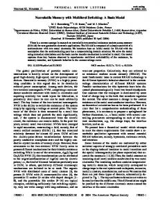
change technology uses a thermally activated, rapid, reversible change in the structure of the alloy to store data. Since the binary information is represented by two different phases of material it is inherently non-volatile, requiring no energy to keep the material in either of its two stable structural states. Amorphous State
Polycrystalline State
Fig. 1. Transmission Electron Microscope images of the two phases of a GeSbTe alloy
The two structural states of the chalcogenide alloy (as shown in Figure 1 are an amorphous state (no long-range order of atoms) and a polycrystalline state (composed of many crystals, each having atoms placed in a repetitive order). Relative to the amorphous state, the polycrystalline state shows a dramatic increase in free electron density (similar to a metal). This difference in free electron density gives rise to a difference in reflectivity. In the case of the rewriteable CD and DVD disk technology, this difference in reflectivity is used to read the state of each memory bit by directing a lowpower laser at the material and detecting the amount of light reflected.
3. CHALCOGENIDE TECHNOLOGY: SEMICONDUCTOR MEMORIES The two phases of the chalcogenide alloy have important differences in electrical properties due to the change in free electron density. The resistivity of the polycrystalline state has been shown to be up to four orders of magnitude lower than that of the amorphous state. Another interesting electrical property of the material is that, above a certain applied voltage (VT), the two states “switch” to a low resistance state that is independent of the material phase (Fig. 3). This switching does not change the structural phase of the material, and the resistance values can be restored once the applied voltage is brought below the “holding” voltage (VH). This phenomenon allows for high current values to be forced through the device with a relatively low voltage that is independent of the phase of the material. These electrical properties are very attractive when considering using a chalcogenide alloy in a semiconductor memory device. The state of such a device can be read non-destructively by charging a capacitively-loaded line through a variable resistance chalcogenide element held at a voltage below VT [8]. The rate of charging – a function of the chalcogenide resistance – can be detected and converted into a logic state. Programming the chalcogenide element is achieved by passing a sufficiently high current (with an applied voltage above VT) to heat the material to the crystallization or melting temperature.
Programming data (by changing the phase of the material) is accomplished by heating the material to an elevated temperature. Depending upon the temperature achieved the material is either melted to form the amorphous state or crystallized by holding it at a lower temperature for a slightly longer period of time (Fig. 2). For the CD and DVD technology, the heat is generated from a high power laser.
Amorphizing RESET Pulse t1
Temperature
Tm
Crystallizing (SET) Pulse Tx t2
Fig. 3. I-V characteristics of chalcogenide
Ta
Time
Fig. 2. Chalcogenide programming
Electrically addressable chalcogenide memory elements have been built to show proof of concept of a chalcogenide-based semiconductor memory. Figure 4 demonstrates the ability to electrically change the resistance of the chalcogenide element by passing a
current through the device. For low currents the device resistance is independent of current and is only a function of the initial state of the material. For moderate currents the temperature of the device is high enough to crystallize the amorphous material, causing its resistance to drop. For higher currents the temperature is high enough to melt the polycrystalline material, increasing the resistance. It is important to realize that for each point on this graph, the resistance is not measured at the indicated programming current, but rather the programming current is applied and then the device resistance is measured at a low current value (0.1mA).
Figure 5 shows that at temperatures as high as 150°C a resistance spread of at least 40x can be maintained for the two phases of the material. This spread increases at lower temperatures. Figure 6 shows that it is projected that data stored in chalcogenide resistors could be retained for 10 years of continuous operation at approximately 125°C. Data retention at typical operating temperatures would be considerably longer.
Unlike flash non-volatile memories, where long erase sequences are needed prior to writing data, chalcogenide elements can be directly over-written without the need for first erasing the previous stored state. Programming of these chalcogenide memory elements has been achieved with pulse widths as small as 3ns.
Fig. 6 Data retention given as an Ahrennius time-temperature relationship
Fig. 4 Electrical programming of chalcogenide
Because of their proliferation in today's powerful computational systems, the cost of semiconductor memories is an important consideration. For chalcogenide-based memories the manufacturing cost should be very low. As the volume of the chalcogenide element decreases, the programming current (power) is reduced and the memory element cell operates more quickly. Chalcogenide-based memory cells have been designed that would be smaller than DRAM cells. Fabrication of the chalcogenide element itself requires between two and four masking steps in a planar topology. These steps are performed after the support or logic transistors have been completed and do not require any process changes that would affect the performance of the transistors (unlike DRAM capacitor processing). Chalcogenide memory elements also show the promise of a tremendous decrease in the cell size (and cost) per bit by allowing true storage of multiple bits per memory element. Figure 7 shows that the transition between low and high resistance can be reproducibly achieved in several steps instead of in one abrupt transition. The 16 discrete resistance states shown could store 4 bits in one small chalcogenide element.
Fig. 5 Chalcogenide resistance versus temperature
Resistance (Ohms)
Top Electrode
Chalcogenide
Polysilicon Bottom Electrode
Fig 7. Multiple state storage example showing 16 separate states. For this graph, 10 pulses were performed at each of 16 current/resistance steps, and the overall measurement was repeated 10 times (each state represents 100 separate write/reads).
Fig. 8. Transmission electron microscope image of functional chalcogenide storage element fabricated under the C-RAM program
4. CURRENT PROGRAM DESCRIPTION
Ovonyx Inc. is applying the OUM technology to semiconductor memories under license from ECD. Ovonyx currently has two joint development programs underway, one with Intel Inc. and one with Lockheed Martin Corporation at its Space Electronics & Communications (LMSEC) site in Manassas, Virginia. The following describes the LMSEC activity that is being funded by the Space Vehicles Directorate of the Air Force Research Laboratory. The Chalcogenide-based Random Access Memory (CRAM) program began in November of 1999 with the goal of integrating the phase-change material into a radiationhardened digital CMOS fabrication process. The program aims at reducing the switching currents required to change device state and then integrating the results into a memory chip of significant density. The program will first develop a memory cell that exhibits switching at under 1 mA in 20ns or less, and then integrate that cell into a high density memory chip using LMSEC’s radiation hardened RHCMOS process. The first demonstration will be a 16Mb chip using 0.5µm lithography by the end of 2002.
Resistance (Ohms)
Energy Conversion Devices (ECD) developed the data described to this point during the late 1990’s. This work concentrated on devices in the 1µm device size range and generally yielded switching currents in the 20mA region. Devices with lower switching currents were made using e-beam lithography for one photo level, but the devices were still overly large in size. In order to be able to make high-density memory chips using this technology it was necessary to change the structure of the device to significantly reduce the overall area, and to reduce the switching currents to below 1mA.
1E+7 1E+6 1E+5 1E+4 1E+3 0.0E+0
2.0E-4
4.0E-4
6.0E-4
8.0E-4
1.0E-3
Current (A)
Fig. 9. Typical R-I plot for C-RAM devices
5. RESULTS TO DATE Experiments conducted at Lockheed Martin’s facility and Ovonyx Inc. facilities in Troy Michigan have shown the feasibility of making C-RAM storage cells with the extremely small size and very low programming currents necessary to construct a memory chip of high density. Storage cells have been constructed and tested using a variety of electrode compositions and physical arrangements of the structures involved, with work continuing at the present time related to optimization of the materials and physical structures as well as gathering reproducibility and cycle life data. Devices exhibiting switching speeds under 50ns with less than 1mA of switching current have been successfully fabricated and tested. These devices typically exhibit two to three orders of magnitude difference in resistance between the set and reset states, and cycle life of up to 1011. A typical device cross section is shown in Figure 8 and typical programming characteristics and I/V curves are graphed in Figures 9 and 10. Figure 11 shows
representative life cycle data. Experiments continue, centered on reducing the variation of the switching current, optimizing cycle life and collecting statistically significant design data to permit design of the 16Mb chip.
total dose levels of 2Mrad, and are planning to follow up with neutron testing of devices later this year. TABLE 2. C-RAM Development Schedule Memory Element Defined Integration with RHCMOS 16M C-RAM Demonstration Qualification of 16M C-RAM
5.0E-4 4.5E-4 4.0E-4
Current (A)
3.5E-4 3.0E-4 2.5E-4 2.0E-4 1.5E-4 1.0E-4 5.0E-5 0.0E+0 0
0.5
1 Device Voltage (V)
Polycrystalline
1.5
Amorphous
Fig. 10. Typical I-V curve for C-RAM devices
12/2000 12/2001 6/2002 12/2002
Development will proceed following the definition of the C-RAM memory element with design of a Comprehensive Technology Characterization Vehicle (CTCV) which will be a test site allowing for the measurement of electrical and other parameters. The CTCV will be useful for demonstration of several drive/sense schemes, which will allow a staged development of the final 16M design. The CTCV will also serve as the vehicle to demonstrate successful integration of the chalcogenide module with the RHCMOS process and will be suitable for radiation testing of the integrated technology in the various radiation environments of interest.
Resistance (Ohms)
ACKNOWLEDGMENT The authors wish to thank the Space Vehicles Directorate of the Air Force Research Laboratory for their technical and financial support of the C-RAM program.The authors also acknowledge the contributions of Lockheed Martin’s STC manufacturing line, and those of Mr.Tyler Lowrey, and the process support and testing support organizations from Ovonyx.
1.E+08 1.E+07 1.E+06 1.E+05 1.E+04 1.E+03 1.E+02 1.E+0 1.E+2 1.E+4 1.E+6 1.E+8 1.E+10
REFERENCES
Cycles [1]
Fig. 11. Typical cycle life for C-RAM devices
[2]
6. FUTURE PLANS
[3]
The schedule for development work leading up to the fabrication and test of a 16Mb C-RAM chip as envisioned under the C-RAM program are given in Table 2, assuming full funding of the various phases of the work including integration and design activities. The process into which the chalcogenide cell will be integrated is the 0.5µm LMSEC RHCMOS process that has been QML qualified at the 5V and 3.3V power supply levels. Both of these process variants are radiation hardened and no degradation of that hardness level is expected as a result of the combining of the technologies. Radiation testing of chalcogenide storage devices in the total dose environment has been reported by Bernacki et al [9]. They reported no observable effects on stored data up to
[4] [5]
[6]
[7]
[8]
S. R. Ovshinsky, "Phase change for optical storage," Business and Technical News from Balgers Materials, Issue 9, October 1999. S. R. Ovshinsky and H. Fritzsche, "Amorphous semiconductors for switching, memory, and imaging application," IEEE Trans. Elect. Dev. vol ED-20, no. 2, pp. 91-105, Feb. 1973. S. Ovshinsky, “Reversible electrical switching phenomena in disordered structures,” Phys. Rev. Lett, vol. 21, no. 20, pp. 14501453, Nov. 11, 1968. H.Fritzsche, “Electronic phenomena in amorphous semiconductors”, Annual Review of Materials Science, v2, pp. 697-744, 1972. S. R. Ovshinsky, S. J. Hudgens, W. Czubatyj, D. A. Strand, and G. C. Wicker, “Electrically erasable memory elements having improved set resistance stability,” US Patent # 5,414,271, May 1995. Hernandez, J., Chao, B., Strand, D., Ovshinsky, S., Pawlik, D., Gasiorowski, P., “Crystallization Studies of Ge:Sb:Te Optical Memory Materials”’ Appl. Phys. Comm., V11, #4, pp557-581, 1992. Yamada, N., Ohno, E., Nishiuchi, K., Akahira, N.,Takao, M., “Rapid-Phase Transitions of GeTe-Sb2Te3 Pseudobinary Amorphous Thin Films for an Optical Disk Memory”, J. Appl. Phys., v69 #5, pp2849-2857, 1991. S. Tyson, G. Wicker, T. Lowrey, S. Hudgens and K. Hunt, “Nonvolatile, high density, high performance phase change
[9]
memory”, Proceedings 2000 IEEE Aerospace Conf., Big Sky MT, Mar. 18-25 2000. S. Bernacki, K. Hunt, S. Tyson, S. Hudgens, B. Pashmakov, and W. Czubatyj, "Total dose radiation response and high Temperature imprint characteristics of chalcogenide based RAM resistor elements" IEEE Trans. Nucl. Sci., vol. 47, no. 6, Dec. 2000
Jonathan D. Maimon received the B.S. degree in chemistry from The College of William and Mary in 1983 and the M.S. degree in chemical engineering from Purdue University in 1985. From 1985 to 2000 he worked as a manufacturing engineer and then as a process development engineer developing radiation-hardened CMOS processes for IBM’s Federal Systems Division, which transferred during this period to Loral and then Lockheed Martin. During this time frame he developed processes for radiation-hardened FPGAs and 64K, 256K, 1M, and 4M SRAMs. Since March 2000 he has been working with Ovonyx as Director of Process Development.
Edward J. Spall received the BSEE degree from the University of Detroit in 1963, and has worked in the semiconductor electronics industry for over 35 years beginning with 31 years at IBM where he held various design and managerial positions with the Federal Systems Division of IBM. While at IBM he designed circuitry for ICBM guidance computers and initiated and managed the semiconductor design and process fab activities at IBM Manassas for 18 years. Mr Spall oversaw the development of CMOS 64K, 256K and 1M SRAM and 16 & 32 bit Microprocessor devices which were radiation hardened to natural and strategic radiation levels and which now operate in a host of NASA, Military and commercial satellites. Mr Spall was Director of Technology at Loral and Lockheed Martin after successive sales of the business to those companies, retiring from Lockheed Martin in November 1999. Mr. Spall then joined Ovonyx Inc. as Director of Manassas Operations involving development of the OUM technology in conjunction with Lockheed Martin.
Robert M. Quinn received the B.S., M.S., and Ph.D. degrees in electrical engineering from Renseselaer Polytechnic Institute in 1963, 1965, and 1968, respectively. Dr. Quinn has worked in commercial silicon semiconductor process development and manufacturing for over 30 years, primarily at IBM Technology Development in East Fishkill, NY, and Essex Junction, VT. His experience ranges from 72Kbit, 5um DRAM through 64Mbit, 0.25um DRAM, with logic and SRAM derivatives from those programs beginning in the 2um silicon gate era. During his employment, he has held various Senior Engineering, Staff, and Managerial positions in development and manufacturing. Currently, Dr. Quinn works at Lockheed Martin Corporation in Manassas, VA, in Advanced Digital Solutions, where he is the Lead Technologist for their radiation hardened CMOS semiconductor development and manufacturing line.
Steven G. Schnur received the BS in Physics degree from the University of Central Florida in 1970. Mr Schnur held process engineering positions at Martin Marietta in Orlando Florida From 1970 to 1974 and at Westinghouse in Lithicum Md from 1974 through 1980 where he was responsible for lithographic process engineering of CCD, Bipolar and CMOS processes. Mr Schnur then moved to IBM in Manassas Virginia where he progressed from process engineering through management assignments in the company’s VLSI rad hard CMOS development and production line where he worked on 64K, and 256K SRAM development and manufacturing. In 1990 Mr Schnur was named program manager of the X-Ray lithography program at IBM and was responsible for a $107M development effort which resulted in the production of deep submicron X-ray lithography which was demonstrated at IBM’s Advanced X-ray facility at Fishkill N.Y. Since 1999 Mr Schnur has been Manager of process development in the Lockheed Martin Space Electronics & Communications Silicon Technology Center at Manassas Virginia which produces memory, microprocessor, ASIC, FPGA and related electronic devices for the military and civilian space market.