cell using magnetic tunnel junctions (MTJs) with magnetic-field-free ... random access memory (MRAM) in power domains instead of SRAM and FF. ... to important memory devices, such as the module configuration register, general purpose.
Nonvolatile Static Random Access Memory (NV-SRAM) Using Magnetic Tunnel Junctions with Current-Induced Magnetization Switching Architecture Shuu’ichirou Yamamoto1,4 and Satoshi Sugahara2,3,4 1
Department of Information Processing, Tokyo Institute of Technology, Yokohama 226-8502, Japan
2
Imaging Science and Engineering Laboratory, Tokyo Institute of Technology, Yokohama 226-8503,
Japan 3
Department of Electronics and Applied Physics, Tokyo Institute of Technology, Yokohama
226-8502, Japan 4
CREST, Japan Science and Technology Agency, Kawaguchi 332-0012, Japan
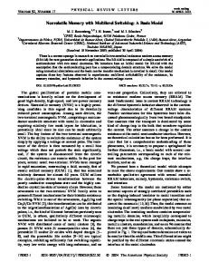
Abstract: We propose and computationally analyze a nonvolatile static random access memory (NV-SRAM) cell using magnetic tunnel junctions (MTJs) with magnetic-field-free current-induced magnetization switching (CIMS) architecture. A pair of MTJs connected to the storage nodes of a standard SRAM cell with CIMS architecture enables fully electrical store and restore operations for nonvolatile logic information. The proposed NV-SRAM is expected to be a key component of next-generation power-gating logic systems with extremely low static-power dissipation. 1. Introduction In recent years, power dissipation has been one of the most important concerns for highly integrated advanced complementary metal-oxide-semiconductor (CMOS) logic circuits, since it constrains their performance and the degree of device integration. In general, power dissipation in CMOS logic circuits can be divided into two components, dynamic and static power. The former is caused by on-current passing through CMOS logic gates due to logic operations, and the latter by leakage current in the CMOS gates during standby mode. The magnitude of the leakage current in CMOS gates is exponentially small in comparison with the on-current. However, static power dissipation gives rise to severe problems for CMOS logic circuits with very large scale integration. Recently proposed power-gating architecture based on multithreshold voltage CMOS (MTCMOS) technology is expected to be very effective at reducing static power dissipation in CMOS logic circuits.1-7 In this type of architecture, logic circuits on a chip are partitioned into several circuitry domains, so-called power domains that are electrically separated from power supply lines and/or ground lines by sleep transistors, and these domains can be shut down during standby periods. Static power is thereby drastically reduced. A key technology for realizing power-gating systems is the backup of logic information in power domains. Static random access memory (SRAM) and its
related latch circuits including a flip-flop (FF) play an essential role in data latches for high-speed logic circuits. However, these memory devices cannot be shut down without losing information. In addition, SRAM and FF dissipate static power during data retention owing to the presence of leakage current in their constituent CMOS gates. The recently developed embedded SRAM array in a microprocessor has the capability of entering "sleep" standby mode, thereby reducing the magnitude of supply voltage to the minimum value required for the memory cells to retain data.3-6 However, this technique cannot reduce the static power to zero. One approach to realizing power-gating architecture for circuitry domains that require no power during standby is to transfer key information from the SRAM/FF in the power domains to a backup SRAM/FF placed in continuously powered circuitry before the power domains are shut down.3,4,7 However, this architecture requires an inconvenient and complicated access procedure for data transfer through a signal bus line or a specially added one-to-one data transfer line. The limited data transfer rates of bus lines and the complex interconnected wiring of one-to-one data transfer lines are not suitable for power-gating systems with power domains that are frequently switched on and off. Another approach is to use nonvolatile memory such as ferroelectric random access memory (FeRAM) and magnetoresistive random access memory (MRAM) in power domains instead of SRAM and FF. However, these memory devices cannot easily replace SRAM and FF, since the operation speed of these devices cannot easily satisfy the requirements of SRAM and FF applications. Therefore, nonvolatile SRAM (NV-SRAM) and nonvolatile FF (NV-FF) with high performance comparable to that of standard SRAM and FF are indispensable for power-gating logic systems. One of the most important applications of NV-SRAM and NV-FF is in nonvolatile power-gating processors as shown in Fig.1, which can be realized by applying NV-FF and NV-SRAM to important memory devices, such as the module configuration register, general purpose register, cache memory, and local storage memory. NV-SRAM and NV-FF can be shut down without losing data, and thus can enable efficient power-gating with domains that require no power during standby, leading to a drastic reduction of static power dissipation. Each power domain of the processor has the ability to execute a fast state transition between normal operation mode and "shutdown" mode, since NV-SRAM and NV-FF require no data transfer to backup memory devices. Using a power management unit to control the sleep transistors of the power domains, NV-SRAM and NV-FF make it possible to establish effective run-time power gating. Combined with a high-density nonvolatile memory (such as MRAM) as the main memory, a dynamic power-gating computing system can be established, as shown in the figure. It should be noted that the nonvolatile feature of the main memory is also beneficial, since it require no program/data loadings from external memory (such as a hard disk drive), when the computing system restarts to execute the suspended operation of a previous powered-on period.
NV-SRAM utilizing a standard SRAM cell with ferroelectric capacitors or resistive switching devices has already been demonstrated.8-11 Magnetic tunnel junctions (MTJs) are an alternative promising candidate as a nonvolatile storage element for NV-SRAM. The Recent development of very high tunneling magnetoresistance (TMR) ratios at room temperature12-14 is useful feature for MRAM15-17 and would also be applicable to NV-SRAM. Although NV-SRAM cells using MTJs have already been reported,18-20 they employ a magnetic field for magnetization switching of the MTJs, induced by current through the interconnections of the circuit. Thus, they potentially have serious problems for programming power, and programming disturbs (that is a technical term of failure mechanism for programming error). On the other hand, magnetic-field-free current-induced magnetization switching (CIMS) technology21-26 allows fully electrical programming for MTJs, and it is expected that the problems of programming power and disturbs can be solved by CIMS technology. The circuit configuration of the above-described NV-SRAM cells using field-induced magnetization switching (FIMS)18-20 cannot be applied to CIMS architecture, since MTJs in the cells using FIMS are placed in their inverter loop, and thus bidirectional current (which is required for CIMS from parallel to antiparallel magnetization and from antiparallel to parallel magnetization) is hardly generated. In this paper, we propose and computationally analyze a new NV-SRAM cell using a pair of MTJs with CIMS architecture for fully electrical nonvolatile information storage. 2. Proposed NV-SRAM cell Figure 2(a) shows the proposed NV-SRAM cell. The cell consists of two cross-coupled CMOS inverters with two pass transistors and a pair of MTJs. The cross-coupled inverters act as a bistable circuit; that is, a circuit that has two stable operating states that correspond to the logic information of 0 (a low voltage level, hereafter denoted by L) and 1 (a high voltage level, hereafter denoted by H). The pass transistors connected to the two storage nodes Q and /Q act as data-access transistors. The two MTJs are also connected to the two storage nodes. Logic information in the bistable circuit can be electrically stored as a magnetization configuration of these MTJs by CIMS using a pulse signal applied to the control (CTRL) line shown in Fig. 2(a), and thus the NV-SRAM cell can be powered off during shutdown mode without losing logic information. When the cell returns to the normal SRAM operation mode, the information stored in the MTJs is quickly restored to the corresponding logic state of the bistable circuit. This can be achieved as a result of the difference in the charging speed of the two storage nodes, owing to the asymmetry of resistances of the two MTJs. Note that NV-latch and NV-FF cells can be realized by connecting capacitive or resistive nonvolatile memory elements to the storage nodes of an inverter loop.27-29 However, there have also not been yet any reports on NV-latch and NV-FF using MTJs with CIMS architecture.
NV-latch and NV-FF cells can also be easily configured in the same manner as the present NV-SRAM cell using a pair of MTJs. Figure 2(b) shows a positive edge triggered master-slave nonvolatile delay-FF (NV-DFF) that consists of a conventional latch and an NV-latch, as indicated in the figure. 3. Device modeling and simulation procedure In order to analyze the circuit operation of the proposed NV-SRAM cell, we developed a SPICE (simulation program with integrated circuit emphasis) macromodel of an MTJ device including CIMS.30 The fundamental circuit of our model consists of variable resistors and current-controlled ideal switches. The concept of the circuit model is similar to the model reported by Zhao et al.31 However, our MTJ model can closely fit the electrical characteristics of recently developed CoFeB/MgO/CoFeB MTJs,14 and includes CIMS phenomenon (discussed later). Figures 3(a) and 3(b) show the current-voltage and resistance-voltage characteristics of the developed MTJ model, respectively. The positive-current direction is defined by the direction from the free layer to the pinned layer in the MTJ model (denoted by f and p, respectively, in the inset of Fig. 3(a)). The junction resistances Rap(0) and Rp(0) of the MTJ model in the antiparallel and parallel magnetization configurations at zero bias voltage were set to 16.7 and 8.33kΩ, respectively, resulting in a TMR ratio (=[Rap(0)-Rp(0)]/Rp(0)) of 100%. This relatively high TMR ratio is easily achieved by recently developed MgO tunnel barrier technology.12-14 MgO-based MTJs with a high TMR ratio showed nonlinear tunneling-type (Simons' formula type) current-voltage characteristics in the antiparallel magnetization configuration, and ohmic-like current-voltage characteristics in the parallel magnetization configuration.14,21,22 Therefore, Rap and Rp can be phenomenologically modeled as follows:
R (V ap
R (V p
MTJ
MTJ
)=
R
p
⎛ V MTJ ⎞⎟ , (0) + [ Rap (0) − R p (0)] ⋅ exp⎜ − ⎜ V / ln 2 ⎟ half ⎝ ⎠
) = R p ( 0) ,
(1)
(2)
where VMTJ and Vhalf are the bias voltage applied to the device and the VMTJ value when the TMR ratio is reduced to half its original value, respectively. This model can reproduce the finding that Rap is asymptotically close to Rp at higher voltages. We compared our model with the experimentally obtained electrical characteristics of a MgO-based MTJ reported in ref. 14. Our model reproduced the experimental results within an absolute error of 1.5% and a standard error of 0.9%. In the following simulations, a Vhalf value of 0.5V was used12 unless otherwise stated.
The
previously noted Rp and Rap values were set so that currents through MTJ1 and MTJ2 exceed critical currents ICF and ICR at the desired bias voltage. ICF for CIMS from the antiparallel to parallel magnetization configuration and ICR from the parallel to antiparallel magnetization configuration were set to 30 and -30μA, respectively. (Their corresponding current density JC is 1×10⁶A/cm2,14,21
when the junction area is 0.003μm2.) In general, the switching speed of CIMS depends on the current density through the MTJ. A lower current density causes a lower switching speed and requires a wider pulse duration. This phenomenon was included in our SPICE macromodel as a "switching delay". The switching delay is realized by timer circuitry, which consists of a voltage comparator and a delay circuit, and it can be set to the desired value by changing the resistance-capacitance product of the delay circuit. In this paper, the switching delay was set at a constant value of 1ns,26 that is, shorter than the pulse width of the store signal applied to the MTJs through the CTRL line by a sufficient amount. In actual usages, the pulse width of the store signal may be prolonged to guarantee a successful store operation. In this paper, the sweep rate of the restore signal (VSP) was set to 1V/ns. The rate should be chosen to assure successful restore operation, and a lower rate is preferable for achieving this. Note that a large store-signal pulse width and a low restore-signal sweep rate do not degrade the performance of normal SRAM operation. Figure 3(c) shows the simulated response of the MTJ current when an alternating triangle voltage VMTJ is applied. CIMS hysteresis is clearly reproduced by our model without unwanted switching noise. Operation of the proposed cell including its transition response was analyzed by HSPICE with a 0.07μm gate-length technology model.32 The gate lengths(L)/widths(W) of n-channel and p-channel MOSFETs were set to 0.07/1μm and 0.07/1.5μm, respectively. The wide gates were used in order to readily achieve CIMS. Although the gate width can be reduced by optimizing the circuit design, a drastic reduction of the gate width requires a reduction of JC to achieve CIMS. This is the same situation as the case for MRAM using CIMS (spin RAM or spin transfer torque RAM).21,22 When a relatively low JC value (such as 5×10⁵A/cm2)and a small MTJ (such as 0.001μm2) are assumed, a narrow gate width with a W/L ratio of unity is applicable.33 The threshold voltages Vthp and Vthn of the p-channel and n-channel MOSFETs are -0.21 and 0.19V, respectively. The supply voltage VSP of the CMOS inverters in the cell during normal SRAM operation was set to 1V. In our simulation, the CTRL line is grounded, floating of the CTRL line or applying a small voltage to the CTRL line can also be appropriate to reduce unwanted leakage current through the MTJs of the NV-SRAM cell during normal SRAM operation. (A related discussion is presented in section 4.3.) 4. Results and discussion 4.1. Store operation of NV-SRAM Operation of the NV-SRAM cell during normal SRAM operation proceeds in the same manner as an ordinary SRAM. The store operation can be performed only by applying a pulse signal to the CTRL line, when the bistable circuit is in one of the stable logic states. Figures 4(a) and 4(b) show schematic illustrations of the store operation of the proposed NV-SRAM cell, where the CTRL
line is at levels L and H, respectively, and Fig. 4(c) shows taht of the restore operation (discussed latter). In Figs. 4(a) and 4(b), the stored information of node Q is at level H and that of node /Q is at level L. The magnetization configuration of both MTJ1 and MTJ2 is antiparallel, which is realized by the operation of data reversal of the bistable circuit during normal SRAM operation, as shown in the last part of the time chart of Fig. 5. (Note that RJ2 (RJ1) shown in Fig. 5(a) (Fig. 5(b)) is less than Rap(0).) This is due to the bias dependence of Rap expressed by eq. (1). The store operation is independent of the initial magnetization configurations of MTJ1 and MTJ2, as described later. IJ1 and IJ2 in Fig. 4 represent currents through MTJ1 and MTJ2, respectively. The positive-current direction of IJ1 and IJ2 is the direction from the free layer to the pinned layer of MTJ1 and MTJ2, respectively, as described previously. It should be noted that in the parallel (antiparallel) magnetization configuration, a negative (positive) current induces CIMS but a positive (negative) current does not, as shown in Figs. 3(a) and 3(b). Figure 5(a) shows simulated waveforms of the NV-SRAM cell, where the time evolution of voltages on the WL, VSP, and CTRL lines, and of voltages VQ and V/Q at nodes Q and /Q, respectively, are plotted. Changes in the magnetization configurations of MTJ1 and MTJ2 are also respectively shown by RJ1 and RJ2 in the figure. Before the application of a signal to the CTRL line, negative IJ1 flows since the CTRL line is grounded and VQ=H [Fig. 4(a)], and thus RJ1 remains at Rap. RJ2 also maintains its initial value, since IJ2 cannot flow through MTJ2 because V/Q=L [Fig. 4(a)]. When a store signal on the CTRL line pulls up to level H, positive IJ2 can flow [see Fig. 4(b)] and RJ2 simultaneously decreases to Rap(VMTJ=H), as shown in Fig. 5(a). Since IJ2 is designed to exceed ICF under this bias condition, the magnetization configuration of MTJ2 switches to parallel after the switching delay, resulting in RJ2=Rp. In contrast, the magnetization configuration of MTJ1 does not vary because VQ=H, although the resistance RJ1 increases from Rap(VMTJ=H) to Rap(VMTJ=0) during the application of the CTRL signal, as shown in Fig. 5(a). As a result of the application of the store pulse to the CTRL line, the node information of VQ=H is transferred into MTJ1 as the antiparallel magnetization configuration (RJ1=Rap), and the node information of V/Q=L is transferred into MTJ2 as the parallel magnetization configuration (RJ2=Rp). It should be noted that if RJ1=Rp before the application of a store pulse, negative IJ1 that exceeds ICR causes CIMS, and thus RJ1 changes from Rp to Rap. However, if RJ2=Rp in the initial state, positive IJ2 induced by a CTRL pulse does not cause CIMS, and thus RJ2 does not change. Therefore, the store operation is independent of the initial magnetization configurations of MTJ1 and MTJ2. When VQ=L and V/Q=H, these logic data are also transferred into MTJ1 and MTJ2 via the mechanism described above, as shown in Fig. 5(b). 4.2. Restore operation of NV-SRAM The restore operation to return to a normal SRAM operation mode is also simple. The VSP line connected to INV1 and INV2 for power supply is pulled up, while the WL line is maintained at
level L. Figure 4(c) schematically shows the charge and discharge current flows with respect to storage nodes Q and /Q. In this figure, Cs1, Cg1, Cs2, and Cg2 represent parasitic capacitances at nodes Q and /Q, which consist of wiring, gate-bulk overlap, and gate-source overlap capacitances in the p-channel and n-channel MOSFETs (ML1, ML2, MD1, and MD2) of INV1 and INV2. VQ and V/Q at storage nodes Q and /Q are given by
V
Q
V
/Q
=
C V C
SP
C V C
SP
s1
+
sg1
=
s2
sg2
+
1
∫C
sg1
1
∫C
sg2
( I L2 −
I
D2
−
I
J1
( I L1 −
I
D1
−
I
J2
)dt ,
)dt ,
(3) (4)
where Csg1=Cs1+Cg1 and Csg2=Cs2+Cg2. IL1 (IL2) and ID1 (ID2) represent the charge and discharge currents with respect to node Q (/Q) through the p-channel and n-channel MOSFETs of INV1 (INV2), respectively. Simulated waveforms exhibited during the restore operation are also shown in Fig. 5(a), and the details of time evolution of VQ, V/Q, VSP-VQ, and VSP-V/Q are shown in Fig. 6(a), where VSP increases from 0 to level H. Figure 6(b) shows the TMR ratio of MTJ1 during the restore operation. In the initial stage of the restore operation (region I denoted in Fig. 6(a)), the charging of nodes Q and /Q is governed by the first terms of eqs. (3) and (4), and nodes Q and /Q are simultaneously discharged by IJ1 and IJ2, respectively. In this region, the charge and discharge currents IL1, IL2, ID1, and ID2 are negligible, because all the MOSFETs are in a cut-off condition. Since it can be assumed that Cs1≈Cs2 and Cg1≈Cg2 owing to the device and circuit symmetries and to the similar bias conditions of both inverters INV1 and INV2 during this stage, both VQ and V/Q gradually increase. However, VQ is always higher than V/Q. This is due to the difference in the discharge rate between Q and /Q, which is because RJ1(=Rap)>RJ2(=Rp), and thus IJ1IL1. This accelerates the charging of node Q, and the voltage difference between VQ and V/Q is enhanced.
Eventually, VQ
becomes higher than the threshold voltage Vthn1 of MD1. Thus, MD1 is turned on, while ML1 is turned off [region III in Fig. 6(a)]. Namely, node /Q is discharged by MD1, and V/Q is further reduced. This
leads to a further increase in the charging of VQ by ML2, and thus MD2 cannot be switched on. During this stage, the TMR ratio of MTJ1 decreases to ~60%. However, the reduction of the TMR ratio has no serious impact on the restore operation, since the current drive capabilites of INV1 and INV2 become higher than those of MTJ1 and MTJ2 in region III, and an initial complementary push-pull operation of INV1 and INV2 is established; that is, VQ and V/Q are in a bistable condition governed by the two inverters, although VQ does not reach level H. Subsequently, V/Q rapidly approaches level L, and VQ increases to level H with increasing VSP [region IV in Fig. 6(a)]. The operating points of MD1 and ML2 enter their linear region. Finally, the feedback loop with the bistable condition of VQ≈H (VQ is lower than level H owing to leakage current through MTJ1 or MTJ2, as discussed later) and V/Q=L is established, which correspond to the information stored in MTJ1 and MTJ2. After the restore operation, the normal mode of SRAM operation is possible. 4.3. Effect of MTJ on normal SRAM operation A disadvantage of the proposed NV-SRAM cell is the flow of current between the level H storage node and the grounded CTRL line through MTJ1 or MTJ2 during normal SRAM mode operation. This leakage current results in excess power dissipation. The circuit current ICELL through the NV-SRAM cell can be defined by IL1+IL2 which include the leakage current induced by MTJ1 or MTJ2, is shown in Fig. 5(a). For the retention of data during the normal operation mode, the NV-SRAM cell requires an ICELL value of 87.6μA. Note that it decreases to 0.14μA when MTJ1 and MTJ2 are decoupled from nodes Q and /Q, respectively. The maximum value of ICELL is 451μA, which is caused by a normal SRAM operation of data reversal, owing to short circuit currents passing through the inverters. As shown in the last part of the time chart in Fig. 5, the operation of data reversal induces CIMS for one of the MTJs with the parallel magnetization configuration. As a result, both RJ1 and RJ2 develop the antiparallel magnetization configuration during normal operation mode (subsequent to the first reversal of data stored in the inverter loop). Obviously, a high Rap value can reduce the unwanted leakage current passing through MTJ1 or MTJ2, and a high Vhalf value is also effective at reducing the leakage current. However, since an increase in Rap with a high Vhalf value requires a high bias for CIMS, the Rp and Vhalf values must be carefully optimized in view of the trade-off between the leakage current in normal operation mode and the bias required for CIMS. Note that although the parallel magnetization configuration in MTJ1 or MTJ2 is established only during the period following the restore operation but prior to the first reversal of data, as shown in Fig. 5, this situation has no serious problems. Since the storage node connected to the MTJ with the parallel magnetization configuration is always at level L, no serious leakage current is generated. The disadvantage of leakage current through MTJ1 and MTJ2 can be easily overcome by introducing selector transistors between the storage nodes (or CTRL line) and the MTJs, as shown in Fig. 7(a). The inverter loop of the NV-SRAM cell can be electrically separated from the MTJs by the
selector transistors. Thus, the MTJs have no effect on the operation speed and the power dissipation during normal SRAM operation. Another interesting challenge is to utilize a pair of spin transistors, such as a pair of the spin-MOSFETs,34-36 instead of the pair of MTJs, as shown in Fig. 7 (b). Their magnetization-configuration-dependent unique transistor behavior is also suitable for NV-SRAM and NV-FF operations. It is worth noting that the circuit configuration of a selector transistor with the MTJ shown in Fig. 7(a) acts as a spin transistor, referred to as a pseudo-spin-MOSFET,37,38 in which its current drive capability can be modified by the magnetization configuration of the MTJ. 5. Conclusions We propose and computationally analyze an NV-SRAM cell using MTJs with magnetic-field-free CIMS architecture. A pair of MTJs connected to the storage nodes of a standard SRAM cell with CIMS architecture make it possible to execute fully electrical store and restore operations for nonvolatile logic information. The proposed NV-SRAM technology using MTJs with CIMS can be applied to NV-latch and NV-FF, and these nonvolatile devices are expected to be important key components for power-gating logic systems of future high-performance and low-power integrated circuits. Acknowledgment The authors would like to thank Professors H. Maejima and H. Munekata of Tokyo Institute of Technology, Professor K. Inomata of National Institute for Materials Science, and Professor M. Tanaka of the University of Tokyo for fruitful discussions and encouragement. This work was partly supported by a Grant-in-Aid for Scientific Research from Ministry of Education, Culture, Sports, Science and Technology and the Core Research for evolutional Science and Technology (CREST) program of Japan Science and Technology Agency (JST). References [1]
S. Mutoh, T. Douseki, Y. Matsuya, T. Aoki, S. Sigematsu, and J. Yamada, IEEE J.
Solid-State Circuits, vol. 30 (1995) 847-854. [2]
H. Kawaguchi, K. Nose, T. Sakurai, in IEEE ISSCC Dig. Tech. Papers, vol. XLI, Feb.
1998, pp. 192-193. [3]
M. Ishikawa, T. Kamei, Y. Kondo, M. Yamaoka, Y. Shimazaki, M. Ozawa, S. Tamaki, M.
Furuyama, T. Hoshi, F. Arakawa, O. Nishi, K. Hirose, S. Yoshioka, and T. Hattori, IEICE Trans. Electron., vol. E88-C (2004) 528-535. [4]
Y. Kanno, H. Mizuno, Y. Yasu, K. Hirose, Y. Shimazaki, T. Hoshi, Y. Miyairi, T. Ishii, T.
Yamada, T. Irita, T. Hattori, K. Yanagisawa, and N. Irie, IEEE J. Solid-State Circuits, vol. 42 (2007) 74-83.
[5]
S. Rusu, S. Tam, H. Muljono, D. Ayers, J. Chang, B. Cherkauer, J. Stinson, J. Benoit, R.
Varada, J. Leung, R. D. Limaye, and S. Vora, IEEE J. Solid-State Circuits, vol. 42 (2007) 17- 25. [6]
M. Yamaoka, Y. Shinozaki, N. Maeda, Y. Shimazaki, K. Kato, S. Shimada, K. Yanagisawa,
and K. Osada, IEEE J. Solid-State Circuits, vol. 40 (2005) 186-194. [7]
V. George, Symp. High Performance Chips, Aug. 2007, HC19.08.01.
[8]
T. Miwa, J. Yamada, H. Koike, H. Toyoshima, K. Amanuma, S. Kobayashi, T. Tatsumi, Y.
Maejima, H. Hada, and T. Kunio, IEEE J. Solid-State Circuits, vol. 36 (2001) 522- 527. [9]
S. Masui, T. Ninomiya, T. Ohkawa, M. Okura, Y. Horii, N. Kin, and K. Honda, IEICE
Trans. Electron., vol. E87-C (2004) 1769-1776. [10]
W. Wang, A. Gibby, Z. Wang, T. W. Chen, S. Fujita, P. Griffin, Y. Nishi, and S. Wong, in
IEEE IEDM Tech. Dig., Dec. 2006, pp. 1-4. [11]
M. Takata, K. Nakayama, T. Izumi, T. Shinmura, J. Akita, and A. Kitagawa, in Abstr. IEEE
21st Nonvolatile Semiconductor Memory Workshop, 2006, pp. 95-96. [12]
S. Yuasa, T. Nagahama, A. Fukushima, Y. Suzuki, and K. Ando, nature mater., vol. 3
(2004) 868-871. [13]
S. S. P. Parkin, C. Kaiser, A. Panchula, P. M. Rise, B. Hughes, M. Samant, and S.-H. Yang,
nature mater., vol. 3 (2004) 862-867. [14]
J. Hayakawa, S. Ikeda, F. Matsukura, H. Takahashi, and H. Ohno, Jpn. J. Appl. Phys., vol.
44 (2005) L587-L589. [15]
K. Inomata, IEICE Trans. Electron., vol. E84-C (2001) 740-746.
[16]
S. Tehrani, J. M. Slaughter, M. Deherrera, B. N. Engel, . D. Rizzo, J. Salter, M. Durlam, R.
W. Dave, J. Janesky, B. Butcher, K. Smith, and G. Grynkewich, Proc. IEEE, vol. 91 (2003) 703-714. [17]
W. J. Gallagher and S. S. P. Parkin, IBM J. Res. & Dev., vol. 50, (2006) 5-23.
[18]
D. Wang, M. Tondra, A. V. Pohm, C. Nordman, J. Anderson, J. M. Daughton, and W. C.
Black, J. Appl. Phys., vol. 87 (2000) 6385-6387. [19]
K. J. Hass, G. W. Donohoe, Y.-K. Hong, and B. C. Choi, IEEE Trans. Magn., vol. 42
(2006) 2751-2753. [20]
W. Zhao, E. Belhaire, C. Chappert, and P. Mazoyer, Proc. IEEE Computer Society Annu.
Symp. VLSI, 2008, p.40. [21]
M. Hosomi, H. Yamagishi, T. Yamamoto, K. Bessho, Y. Higo, K. Yamane, H. Yamada, M.
Shoji, H. Hachino, C. Fukumoto, H. Nagao, and H. Kano, in IEEE IEDM Tech. Dig., Dec. 2005, pp. 459-462. [22]
T. Kawahara, R. Takemura, K. Miura, J. Hayakawa, S. Ikeda, Y. Lee, R. Sasaki, Y. Goto, K.
Ito, T. Megura, F. Matsukura, H. Takahashi, H. Matsuoka, and H. Ohno, IEEE J. Solid-State Circuits, vol. 43 (2008) 109-120. [23]
G. D. Fuchs, N. C. Emley, I. N. Krivorotov, P. M. Braganca, E. M. Ryan, S. I. Kiselev, J. C.
Sankey, D. C. Ralph, and R. A. Buhrman, Appl. Phys. Lett., vol. 85 (2004) 1205-1207. [24]
J. Hayakawa, S. Ikeda, Y. M. Lee, R. Sasaki, T. Meguro, F. Matsukura, H. Takahashi and H.
Ohno, Jpn. J. Appl. Phys., vol. 44 (2005) L1267-L1270. [25]
H. Kubota, A. Fukushima, Y. Ootani, S. Yuasa, K. Ando, H. Maehara, K. Tsunekawa, D. D.
Djayaprawira, N. Watanabe, and Y. Suzuki, Jpn. J. Appl. Phys., vol. 44 (2005) L1237-L1240. [26]
Y. Huai, D. Apalkov, Z. Diao, Y. Ding, A. Panchula, M. Pakala, L.-C. Wang, and E. Chen,
Jpn. J. Appl. Phys., vol. 45 (2006) 3835-3841. [27]
Y. Fujimori, T. Nakamura, and H. Takasu, Integrated Ferroelectrics, vol. 47:1 (2002)
71-78. [28]
K. Abe, S. Fujita, and T.H. Lee, in Tech. Proc. 2005 NSTI Nanotechnology Conf. Trade
Show, vol. 3 (2005) 203-206. [29]
S. Koyama, Y. Kato, T. Yamada, and Y. Shimada, IEICE Trans. Electron., vol. E89-C
(2006) 1368-1372. [30]
S. Yamamoto and S. Sugahara: in preparation for publication.
[31]
W. Zhao, E. Belhaire, Q. Mistral, C. Chappert, V. Javerliac, B. Dieny, and E. Nicolle, in
Proc. Behavioral Modeling Simulation Conf. 2006, vol. 1 (2006) 40-43. [32]
Device
Group
at
UC
Berkeley,
“Berkeley
Predictive
Technology
Model,”
http://www.eas.asu.edu/~ptm. [33]
S. Yamamoto and S. Sugahara: presented at 53rd Conf. Magnetism and Magnetic Materials,
2008, CT04. [34]
S. Sugahara and M. Tanaka, Appl. Phys. Lett., vol. 84 (2004) 2307-2309.
[35]
S. Sugahara, IEE Proc. Circuits, Device-Systems, vol. 152 (2005) 355-365.
[36]
S. Sugahara, Physica Status Solidi C, Vol. 3 (2006) 4405-4413.
[37]
S. Sugahara and S. Yamamoto: presented at 55th Spring Meet. Japan Society of Applied
Physics, 2008, 30p-F-6. [38]
Y. Shuto, S. Yamamoto, and S. Sugahara: to be published in J. Appl. Phys.
External memory
Nonvolatile main memory (MRAM)
Bus NV-SRAM array
Power management unit
NV-SRAM array
Sleep Tr. NV-FFs
Power domain (module)
Nonvolatile power-gating processor Fig. 1. Schematic illustration of nonvolatile power-gating processor. Combining nonvolatile main memory, a dynamically run-time power-gating computing system can be configured.
D
INV1
Q Pass Tr1
p
MTJ1 f
WL /Q p
INV2
f
Pass Tr2
/D
MTJ2
CTRL
(a) Conventional latch
D
NV-latch CLK
/CLK Pass Gate3
Pass Gate1
INV3
/CLK
CLK CLK
/Q INV1
INV4
Pass Gate4 /CLK
INV2
/CLK MTJ1
CTRL
Q
p f
p
Pass Gate2 f CLK MTJ2
NV-DFF (b) Fig. 2.
Circuit configuration of the proposed (a) NV-SRAM cell and (b) positive edge triggered master-slave NV-DFF.
AP to P
ICF 0 ICR
+ VMTJ f
P to AP
p
Vsource -
Resistance R
MTJ
(kΩ)
-150 -1
IMTJ
0 Voltage VMTJ (V) (a)
1
18 14 AP to P P to AP
10 6 -1
0 Voltage VMTJ (V) (b)
1
150
Voltage V MTJ (V)
1
0
-1
AP to P
0
2
P to AP
4 Time (µs) (c)
6
0
8
Current I MTJ (µA)
Current I MTJ (µA)
150
-150
Fig. 3. (a) Current-voltage and (b) resistance-voltage characteristics of the present MTJ model. The current direction is shown in the inset, where f and p denote the free and pinned layers of the MTJ model, respectively. P and AP in the figure indicate the parallel and antiparallel magnetization configurations, respectively. (c) Simulated response of the MTJ current, when an alternating triangle voltage is applied to the MTJ model.
INV1
VQ=H
off VSP RJ1⇒Rap p INV2 MTJ1 f I J1 CTRL D
V/Q=L
WL off
/D
p R :unchanged J2 f MTJ 2
(a)
INV1
VQ=H
off MTJ1 p RJ1:unchanged f D
INV2
CTRL WL D
off
VSP IJ2
Fig. 4.
off /D VSP p MTJ2 f RJ2 ⇒Rp
(b)
IL2 Cs2 ML2
Cs1
Q I RJ1=Rap D2 p M D2 Cg2 IJ1 f CTRL
WL
V/Q=L
VSP ML1
off /D
IL1
/Q R =R MD1 p J2 p Cg1 ID1 f IJ2 (c)
Schematic illustrations of store operation with (a) level L and (b) level H voltages on the CTRL line. (c) Schematic
illustration of restore operation, where ML1 (ML2) and MD1 (MD2) configure INV1 (INV2).
(a)
Powered-off period Normal SRAM mode Store operation Powered-off operation
1ns WL V SP CTRL VQ V/Q RJ1 RJ2 VQ V/Q RJ1 RJ2
Storage data reversal
H L H L H L H L H L Rap(0) Rap(VMTJ=H) Rp Rap(VMTJ=H) Rap(VMTJ=H) Rap(0) AP to P transition P to AP transition Rp Switching delay
(b)
Restore operation Normal SRAM mode
Switching delay
H L H L Rap(VMTJ=H) Rap(VMTJ=H) Rap(0) AP to P transition P to AP transition Rp Switching delay Switching delay Rap(0) Rap(VMTJ=H) Rp
Fig. 5. Simulated input and output waveforms of the NV-SRAM cell for the store, restore, and normal SRAM mode operations with initial conditions of (a) VQ=H and V/Q=L and (b) VQ=L and V/Q=H.
0.8 0.8 0.7
Region I
II
IV
III
Voltage (V)
0.6
VQ
0.5
VSP
0.4
0.4
VSP-V/Q
0.3 0.2 0.1
00 0 0
V/Q 0.1
0.2 0.2
VSP-VQ
0.4 0.5 0.6 0.4 0.6 Time (ns) (a)
0.3
0.7
0.8 0.8
0.7
0.8 0.8
100 100 90
TMR ratio (%)
80 70 60
5050 40 30 20 10
00 0 0
Region I 0.1
0.2 0.2
II
III
IV
0.4 0.5 0.6 0.4 0.6 Time (ns) (b)
0.3
Fig. 6. (a) Time evolution of the node voltages VQ and V/Q, and their differences with respect to VSP. (b) TMR ratio of MTJ1 during the restore operation.
INV1
Q
D
Pass Tr1 Selector Tr1
WL /Q Pass Tr2
INV2
Selector Tr2
SR p
MTJ1 f
PseudospinMOSFET
p f
MTJ2
CTRL
(a) D
INV1
Q Pass Tr1
SpinMOSFET1
/D
INV2
SR
WL /Q Pass Tr2
/D
SpinMOSFET2
CTRL
(b) Fig. 7. Circuit configurations of NV-SRAM cells using (a) selector transistors and (b) spin-MOSFETs. The SR line is activated only in store and restore operation modes.