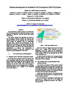
Fermi National Accelerator Laboratory. P.O. Box 500, Batavia, Illinois 60510. November 1998. Published Proceedings of the Fourth Workshop on Electronics for ...
F
Fermi National Accelerator Laboratory FERMILAB-Conf-98/288
Charge Integrator and Encoder ASIC for Readout of the CMS Hadron Calorimeter Photodetectors A. Baumbaugh et al.
Fermi National Accelerator Laboratory P.O. Box 500, Batavia, Illinois 60510
November 1998
Published Proceedings of the Fourth Workshop on Electronics for LHC Experiments, Rome, Italy, September 21-27, 1998
Operated by Universities Research Association Inc. under Contract No. DE-AC02-76CH03000 with the United States Department of Energy
Disclaimer This report was prepared as an account of work sponsored by an agency of the United States Government. Neither the United States Government nor any agency thereof, nor any of their employees, makes any warranty, expressed or implied, or assumes any legal liability or responsibility for the accuracy, completeness, or usefulness of any information, apparatus, product, or process disclosed, or represents that its use would not infringe privately owned rights. Reference herein to any speci c commercial product, process, or service by trade name, trademark, manufacturer, or otherwise, does not necessarily constitute or imply its endorsement, recommendation, or favoring by the United States Government or any agency thereof. The views and opinions of authors expressed herein do not necessarily state or re ect those of the United States Government or any agency thereof.
Distribution Approved for public release; further dissemination unlimited.
Copyright Noti cation This manuscript has been authored by Universities Research Association, Inc. under contract No. DE-AC02-76CHO3000 with the U.S. Department of Energy. The United States Government and the publisher, by accepting the article for publication, acknowledges that the United States Government retains a nonexclusive, paid-up, irrevocable, worldwide license to publish or reproduce the published form of this manuscript, or allow others to do so, for United States Government Purposes.
Charge Integrator and Encoder ASIC for Readout of the CMS Hadron Calorimeter Photodetectors A. Baumbaugh, M. Binkley, X. Y. Chen, J. E. Elias, S. Hansen, S. Los, R. Tschirhart, T. Zimmerman, R. J. Yarema Fermi National Accelerator Laboratory∗ P.O. Box 500, Batavia, IL 60510 Abstract A charge integrator and encoder ASIC is being developed at Fermilab for readout of the CMS hadron calorimeter photodetectors. The chip provides eight nonoverlapping ranges and is pipelined for deadtimeless operation. It is intended to be used with an FADC to digitize hybrid photodiode current pulses at 40 MHz. For each clock period, one range is selected depending on the signal magnitude, and the output of that range is fed to the FADC to form the mantissa. The selected range is encoded and output as a 3-bit digital exponent. Previous versions of this device have been designed for use with photomultipliers which can have high gain. Hybrid photodiodes have gains of only a few thousand so that a new version of the chip is needed which includes a current-mode preamplifier. The principle of the device is described and early results from a demonstrator project are presented. 1. INTRODUCTION Hadron calorimeters (HCAL) in the central and end cap regions of the CMS detector are sampling structures with copper absorber plates and scintillator readout layers. Scintillation light from particle showers is collected and re-emitted by wavelength-shifting plastic fibers embedded in grooves machined into the scintillator tiles. Clear plastic fibers are used to carry the shifted light to the photodetectors located in light-tight enclosures on the outer calorimeter surface. Inside these boxes, the clear fibers that originated from scintillator layers are reorganized to form projective towers of scintillator tiles. Hybrid photodiodes[1] are used as the photodetectors because of the 4 Tesla magnetic field at the readout box position. These devices consist of a photocathode followed by a gap of several millimeters over which a large applied electric field accelerates photoelectrons onto a silicon diode target. The signal is generated by electron bombardment, and the diodes are patterned into pixels to provide many channels in one package, The HCAL readout system must satisfy demanding requirements for rate, dynamic range, and noise floor. The precision of measurement requirement is less critical in accordance with the intrinsic resolution of a hadron calorimeter. Several techniques have been developed and implemented in other experiments that can meet any two ∗
of these three requirements as response bandwidth trades against noise floor and dynamic range. The two approaches finding acceptance today are switched capacitor analog storage arrays and multi-range direct digital techniques. This report describes a direct digital approach which is based on a current-splitter input stage driving a parallel set of identical integrating capacitors, one of which will be selected as within range for digitization. An important characteristic of this approach is that it maintains approximately constant resolution over the full dynamic range. Originally, the current-splitter technique was proposed for calorimeter readout at the Superconducting SuperCollider project[2]. Subsequent events led to development and deployment of these multi-range ASICs in the KTeV experiment at Fermilab[3,4] which features a precision crystal electromagnetic calorimeter with photomultiplier tube readout. The KTeV performance specifications exceed those of prior art. Table 1 indicates the developments needed for the CMS HCAL readout by providing a comparison between the performance numbers of the KTeV system and those for the CMS HCAL requirements. The two areas where performance improvements are needed are apparent, noise floor and sensitivity. Table 1: KTeV and CMS comparison PARAMETER KTEV CMS Range 16 bits 15 bits Least Count 8 fC 0.32 fC Noise 15,000 e’s 3000 e’s Clock 53 MHz 40 MHz 2. REQUIREMENTS Front-end electronics for the HCAL calorimeter reside on the outer surface of the absorber inside readout boxes that also house the optical rearrangement structures and photodetectors. At this location, the ionizing radiation dose is very small amounting to tens of kilorads at most. However, the neutron fluence is not negligible amounting 10 to more than 10 per cm squared per year for kinetic energies above 100 keV. In today’s terms, the electronics is required to be radiation tolerant. Performance requirements follow from a combination of physics issues, collider parameters and calorimeter
Work supported by U.S. Department of Energy under contract no.l DE-AC02-76CHO3000.
characteristics. The most significant of these include: calorimeter energy resolution and photoelectron response, photodetector gain and signal duration, collider crossing frequency, minimum ionizing signal size and highest energy signal expected. Table 2 provides a summary of the operation and performance requirements.
85%/√E ⊕ 5%
Table 2: Requirements summary PARAMETER VALUE Operation Gated integrator Frequency 40 MHz Aperture 25 nsec Charge loss Less than 2% Dynamic range 35,000 to 1 Precision 1% rms Least count 2,000 electrons Noise 3,000 electrons rms Cross talk Less than 2% Gain stability Less than 1%/week Temperature coefficient Less than 0.03%
QIE Resolution 8 range ÷ 3-2 5 bit ADC
Figure 2. Resolution performance. 3. THE QIE ASIC The abbreviation QIE was chosen to indicate charge (Q) integration (I) and encoding (E). Functioning as a gated integrator, the QIE produces two outputs per clock period: a three-bit integer indicating the range and a voltage proportional to the integrated input charge for that range. Coupled with a fast ADC, the QIE front end produces a floating-point result each clock period: m bits of range (exponent) plus n bits of ADC (mantissa). Figure 1. shows an example of a QIE front-end system from the HCAL project where three hybrid photodiode pixels are processed on one small circuit board. Each channel QIE Based HCAL Front End 3
Digital Exponent
QIE Digital Exponent Clock Reset HPD Input Analog MAntissa
40MHz Init Bunch Marker
Clock 5
ADC 3
Clock 5
ADC QIE Digital Exponent Clock Reset HPD Input Analog MAntissa
DIGITAL ASIC
Clock Reset HPD Input Analog MAntissa
Clock 5
Reset DATA
Laser
Optical Fiber
1GBit/S Serializer
Serial Control Path Test Pulse Amplitude
ADC
QIE
Table 3: Range and resolution Range
1 2 3 4 5 6 7 8
Current
Min E GeV
Max E Gev
Bin size GeV
Bin size fC
I I/3 I/9 I/27 I/81 I/162 I/324 I/648
0 2.8 11.2 36.4 112.0 338.8 792.4 1699. 6
2.8 11.2 36.4 112.0 338.8 792.4 1699.6 3514.0
0.1 0.3 0.9 2.7 8.1 16.2 32.4 64.8
0.32 0.96 2.88 8.64 25.92 51.84 103.68 207.36
Clock 24
3 TCk TMS TDI TDO
Multi-range integration of the signal is done using a current splitter input stage coupled to a set of identical capacitors. An input bias current is applied to set the operating point of the splitter transistors and provide a unique pedestal for each range so that a companion set of comparators can unambiguously select the voltage on one range for routing to the FADC.
Test Outs
Figure 1. Front end electronics block diagram. produces an 8-bit result, 3-bits of range plus the result from a 5-bit FADC, to a 24-bit wide serializer operated at 40 MHz clock rate. Figure 2 and Table 3 are provided for visualization of the design parameter choices.
Current splitting is accomplished through a parallel array of common-base NPN transistors and grouping the collectors in the desired weights. An example of a current splitter input stage with binary weights is shown in Figure 3. An external DC bias current is provided to satisfy the comparator requirements and to optimize transistor operating parameters. To maintain performance at small input signals, a feedback amplifier is used at the input with the paralleled transistors of the splitter as the series pass element. In order to maintain constant split ratios over the full dynamic range, the transistor collectors should be held at the same voltage. MOS cascode circuits are used to equalize the collector voltages and pass the current through to the next stage. For large signals, the most sensitive ranges experience very high currents. Series
Iin/2
Iin/4
Iin/8
Iin/16
Iin/64
Iin/32
Vb1
Iin/128 Iin/256
CURRENT LIMITERS
MOS CASCODE CIRCUITS 1 2
128 129 130
192
193 194
224 225 226
240 241 242
248 249 250
252 253 254
Rin
FEEDBACK AMPLIFIER GAIN ELEMENTS
INPUT
Vb2
256
255
Figure 3. Current splitter example. current limiters are installed on each range to prevent overloads to the subsequent circuitry. Deadtimeless operation is another requirement for calorimeter readout at future collider experiments. The QIE incorporates pipelined operations to meet this requirement. A latency of four clock cycles is needed to perform all signal processing operations, and four identical sets of integrating capacitors and comparators are utilized. At any one moment in time, one set is connected to the current splitter, the second set is settling into the comparators, the third set is connected to the outputs, and the fourth set is being reset. The QIE ASICs produced for KTeV have shown that high precision, in terms of settling error, reset residual and charge loss at time slice boundaries, can be obtained with a pipeline only four clocks deep at clock speeds up to ~80 MHz. Present versions of the QIE have been fabricated in a 2 micron Orbit CMOS process. The CMS HCAL devices are planned for an 0.8 micron BiCMOS process to provide higher performance transistors. The development program, which is beginning now, is planned for a two and a half year period with the production run targeted for January 2001. 4. CMS DEMONSTRATOR PROJECT Sensitivity and noise requirements for the CMS application are significantly tighter than those for the KTeV experiment as shown in Table 1. The principal reason for such challenging performance numbers is the difference in calorimeter light yield. The crystals used in KTeV have a very high light yield compared to the scintillator and waveshifter sampling calorimeter of CMS. A demonstrator project was organized to explore these issues both on the bench top and in the test beam with prototype calorimeter modules. Convinced that a
QIE itself could not achieve the needed performance, the project team focused on developing a current-mode inverting preamp for the KTeV QIE system that provided the desired overall sensitivity. Figure 4a shows a block diagram of the amplifier and Figure 4b shows the diagram for the fast pulse amplifier block. The low pass DC-coupled path is required for measurement of the signal produced by a radioactive calibration source illuminating the scintillator tiles. The cross over point between the AC and DC paths is set at 1 kHz.
In
Out
Ri
High Frequency Amp
RL
Rf _ + DC Low Leakage Amp
Figure 4a. Preamplifier block diagram. The demonstrator preamp uses discrete components and was designed with SPICE. Even then, three iterations of printed circuit layout were needed to conquer the problem of parasitics. The QIE and readout artwork was taken straight from KTeV files. The final circuit board footprint was chosen to allow use in the calorimeter readout box and limited the density to six channels per board.
V+
Rf
V+
RE
_
In VB
Out
+
Current Mirror
Figure 4b. High frequency amplifier functional diagram. On the test bench, noise levels were quite low with an rms of about 2200 electrons. The sensitivity is slightly lower than targeted having a 2400 electron least count instead of 2000. For 10 degree temperature excursions about room temperature, the gain temperature coefficient is 0.07%. Since a rather high value of preamp gain, ~ 20, is needed to use the existing QIE chips, the linear dynamic range was slightly more than 50% of full scale, or about 2 TeV in terms of calorimeter energy. This is quite adequate for the test beam, which is limited to 400 GeV. An ASIC optimization of preamp and QIE stages is expected to only require a current gain of about eight making it possible to cover the full dynamic range. In the test beam in August, most of the allotted time was spent trying to solve environmental noise and pedestal stability problems. A compromise was taken to allow data taking in which the noise was beaten down to 7500 electrons rms but the slow pedestal instability remained. Muon, pion and radioactive
source data were taken with the demonstrator electronics at the end of August. The clock was run at 40 MHz but was not synchronized to the accelerator and hence the triggers were randomly phased. Uncorrected histograms of raw data show that the minimum ionizing signal from a single layer of scintillator is clearly seen. The pion signal is seen in several channels as the shower size exceeds the calorimeter cell size. At this time, information on line shape and resolution waits on establishing relative channel gains for summing and on untangling the pedestal instability effects. REFERENCES [1] See the Proceedings of the First Conference on New Developments in Photodetection, Beaune, France, June 24-28, 1996, Section III. “Other Vacuum Devices: Hybrid Photodiodes” which contains 10 papers with extensive references. [2] R. J. Yarema et al, “A High Speed, Wide Dynamic Range Digitizer Circuit for Photomultiplier Tubes”, Nuclear Instruments and Methods in Physics Research A 360 (1995) 150-152. [3] T. Zimmerman & M. Sarraj, “A Second Generation Charge Integrator and Encoder ASIC”, 1995 IEEE Nuclear Science Symposium Volume 1 (1996) 280-284 [4] J. Whitmore, “The Performance of a High Speed Pipelined Photomultiplier Readout System in the Fermilab KTeV Experiment”, Nuclear Instruments and Methods in Physics Research A 409 (1998) 687-690.