966
IEEE TRANSACTIONS ON CIRCUITS AND SYSTEMS—I: FUNDAMENTAL THEORY AND APPLICATIONS, VOL. 49, NO. 7, JULY 2002
Computation of Design Values for Class E Amplifiers Without Using Waveform Equations Hiroo Sekiya, Member, IEEE, Iwao Sasase, Senior Member, IEEE, and Shinsaku Mori, Member, IEEE
Abstract—This paper presents a novel design procedure for Class E amplifiers without using waveform equations. By the proposed design procedure, Class E amplifiers can be designed regardless of the factor of resonant circuit, existence of the switch on resistor, and so on. The proposed design procedure requires only circuit equations and design specifications. All design procedures reported until now require deriving waveform equations which requires a lot of work. The benefits of the proposed design procedure is that it is to deriving waveform equations is no longer necessary. When the circuit equations are obtained, the other procedures for computation of design values are carried out with aid of computer. Therefore, we can design Class E amplifier more easily than the conventional design procedure. The authors design Class E amplifiers by using the proposed design procedures and carry out the circuit experiments, and find that the experimental results agree with calculation results, and show the validity of the proposed design procedure. Index Terms—Class E amplifier, design procedure, Newton’s method, Runge–Kutta method, variational equations.
I. INTRODUCTION
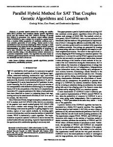
Fig. 1. (a) Circuit topology of Class E amplifier. (b) Equivalent circuit.
C
LASS E switching-mode tuned power amplifiers [1]–[17], frequency multipliers [14], [18]–[20], and dc/dc power converters [21], [22] have become increasingly valuable building blocks in many applications, e.g., radio transmitters and switching-mode dc power supplies. Because of Class E switching, namely, both zero voltage and zero slope of voltage switching, the efficiency of energy conversion is very high at high frequencies. Therefore, a high density of dc/dc power processing can be achieved, reducing the size and weight of the equipment. Since the introduction of the Class E amplifier, many analytical descriptions of this circuit have appeared [1]–[14]. Early analyses assumed an ideal switch, infinite output network (i.e., sinusoidal output current), and an RF choke in the dc supply lead (i.e., constant current drive) [1], [2]. Later works have allowed finite dc-feed inductance [7]–[11], drain current fall time [12], [13], finite output network [3]–[10],
Manuscript received December 9, 2000; revised October 20, 2001. This work was supported by the The Japan Science Society under the Sasakawa Scientific Research Grant. This paper was presented in part at the Midwest Symposium on Circuits and Systems, Dayton, OH, 2001. This paper was recommended by Associate Editor H. S. H. Chung. H. Sekiya is with the Graduate School of Science and Technology, Chiba University, Chiba 263-8522, Japan (e-mail:
[email protected]). I. Sasase is with the Department of Information and Computer Science, Keio University, Yokohama 223-8522, Japan (e-mail: sasase @sasase.ics.keio.ac.jp). S. Mori is with the Department of Electrical and Electronics Engineering, Nippon Institute of Technology, Saitama 345-8501, Japan (e-mail:
[email protected]). Publisher Item Identifier 10.1109/TCSI.2002.800474.
[13] and nonzero active device on-resistance [7] and [18]. In these analyses, the circuit configuration with finite dc-feed inductance, finite output network , and nonzero active device on resistance in [7] and [18], as shown in Fig. 1(b), may be described as a generalized Class E amplifier configuration, since its analysis can provide results for most of the other Class E amplifier configurations published up to the present time. However, this analysis and design need to derive waveform equations whose derivations need a lot of symbolic calculations. If the design procedure of Class E amplifier without using waveform equations is established, the waveforms and the performance of the circuit can be derived easily under the good circuit simulator, e.g., SPICE, numerical calculations and so on. Therefore, the design procedure without using waveform equations is valuable technique in the research of Class E amplifier. This paper presents a novel design procedure for Class E amplifiers. The feature of the proposed design procedure is that the waveform equations are never needed. The design procedure requires only circuit equations and design specifications. When circuit equations are obtained, the other procedures for computation of design values are carried out with the aid of computer. Therefore, we can design Class E amplifier more easily than the conventional design procedure. The concept of the proposed design procedure is that the design values of Class E amplifier is obtained by solving the algebraic equations of transient conditions and those of Class E switching conditions, simultaneously. The proposed design procedure allows finite
1057-7122/02$17.00 © 2002 IEEE
SEKIYA et al.: COMPUTATION OF DESIGN VALUES FOR CLASS E AMPLIFIERS
967
switch. While the switch is on, it is flowing through the switch as . Since the switching loss is reduced to zero by the operating requirements of zero and zero slope of switch voltage and ) at the turn on transition, called Class ( E switching conditions, the theoretical efficiency of Class E amplifier is 100%. The dc-feed inductor is assumed as RF choke in dc supply lead for constant input current in [1]–[6]. In case should be that the small circuit scale is required, however, small. And thus, finite dc-feed inductor needs to be considered. On the other hand, the low loaded quality factor is required for the high output power. Such as these examples, various design specifications are considered for the requirements of the circuit design. Therefore, it is useful to establish the simple design procedure of Class E amplifier which is applied in every specification. B. Design Procedure by Albulet et al.
Fig. 2. Nominal waveform of Class E amplifier.
dc-feed inductance, drain current fall time, finite output network , nonzero active device on-resistance, nonlinear operation of passive elements, and so on, which are all conditions considered until now. Moreover, the design procedure can be applied to the design of Class E frequency multiplier [18]–[20], Class DE amplifier [24], Class DE frequency multiplier [25], phase-controlled Class E amplifier and Class E frequency multiplier [15]–[17], and so on. We design Class E amplifier by using the proposed design procedure and carry out the circuit experiments. We can find that the experimental results agree with calculation results, and show the validity of the proposed design procedure. II. CLASS E AMPLIFIER A. Principle Operation Fig. 1 depicts the circuit topology of Class E amplifier. It con, a dc-feed inductor , sists of an input direct voltage source shunting the switch, a series resa switch and a capacitor , and an output resistor . The waveforms onant circuit of Class E amplifier are shown in Fig. 2, when switch on duty in ratio is 50%. The switch is driven by a driving pattern of is large, the input current Fig. 2. If the dc-feed inductance of the amplifier is approximately constant, which is equal to its , dc component. If the loaded quality factor is high resonant circuit is approximately a the current through the sine wave. As shown in Fig. 2, while the switch is off, the current across the through the shunt capacitor produces the voltage
In this section, we summarize a design procedure by Albulet et al. [14], [18]–[20] which is applied to various configurations of Class E amplifier, and we point out its problems. At first, the analysis for design is based on the following assumptions. 1) The switching device has zero switching times and infinite off resistance. 2) All passive elements are ideal. is independent of the switch 3) The shunt capacitance voltage and includes any device capacitance. The equivalent circuits are constructed from assumption 1, as shown in Fig. 1(b). The equivalent circuit is usually classified into two cases by the states of the switch, namely, on or off. Therefore, circuit equations in case of on and off states are formulated, respectively. Since the circuit equations are linear differential equations from assumptions 2 and 3, they are solved strictly and waveform equations are derived. The characteristic polynomial is, however, three- or four-dimensional equations. Therefore, it is very difficult to derive the roots of the characteristic polynomial analytically, and we need to assume that the roots are known and one of the following conditions is true in case of four-dimensional characteristic polynomial: 1) four real roots; 2) two real roots and a pair of complex conjugates; or 3) two pairs of complex-conjugate roots. As a result, we need to solve the circuit equations for above three cases, and have a lot of works since the resulting equations of waveforms are complicated. Moreover, if the assumption 2 is not assumed, the waveform equations cannot be derived. The derivation of the waveform equations is one of the problems about this design procedure. The next step of the design is to eliminate initial conditions in each case from the transient conditions, namely, continuities of the current and the voltage between on and off states. And finally, the circuit parameters are found from Class E switching conditions. The second problem of the design procedure is that it is never established how to find the solutions of the algebraic equations which are transient conditions and Class E switching conditions. The general technique to solve algebraic equations is Newton’s method. Though Newton’s method require Jacobian matrix of the equations, the Jacobian matrix cannot be derived in this case. That is because the waveform equations include the
968
IEEE TRANSACTIONS ON CIRCUITS AND SYSTEMS—I: FUNDAMENTAL THEORY AND APPLICATIONS, VOL. 49, NO. 7, JULY 2002
roots of characteristic polynomial that is not expressed analytically. Therefore, Newton’s method cannot be applied to solve the algebraic equations in this case. III. THEORY OF DESIGN PROCEDURE In this section, the theory of the proposed design procedure is presented.
C. Other Conditions For design of the amplifier, we often consider several conditions, i.e., zero voltage switching, zero current switching, Class E switching conditions, and so on. If the number of conditions is , the conditions that consist of each condition at are expressed as
A. Circuit Description Let us consider a dynamic circuit described by a differential equations (1) , , and denote the time, an where -dimensional state and an -dimensional system parameter, respectively. In this paper, For simplicity
(6)
.. .
design parameters. Therefore, the In this case, we can find parameters must be given as the design specifiother cations. From design procedure of Section II-B, we recognize that the design of the amplifier boils down to the derivation of the solution of the algebraic (5) and (6). These equations are rewritten as follows:
(2) (7) is assumed as
mapping and is periodic in with period
: (3)
We also assume that (1) has a solution with every initial condition fined on and every .
de-
where,
,
and
are
expressed
. Moreover, we define
are unknown design parameters in
B. Poincaré Map and Fixed Point By the periodic hypothesis (3), we can naturally define a diffeomorphism from state space into itself
(8)
D. Computation of Design Values (4)
The mapping is often called the Poincaré mapping. is periodic with period If a solution is a fixed point of point
, as
as , and
, the
We solve the (7) by using Newton’s method that is the general algorithm to solve the algebraic equations. Since the unknown , the values of (7) are expressed as computations (9)
(5) , (5) corresponds to the transient conditions in the If design procedure of Section II-B.
in order to find the unknown are iterated for means Jacobian matrix of values, where , that is, we obtain (10) shown at the bottom of the page, is a
.. . (10)
.. .
SEKIYA et al.: COMPUTATION OF DESIGN VALUES FOR CLASS E AMPLIFIERS
iteration number and , i.e., in this paper. Then is a solution of (7). by applying For computations of (9), we can derive Runge–Kutta method to (1). And the elements of Jacobian maof (10) can be determined by solving the first-order trix variational equations [23] with
969
4)
: The ratio of the resonant frequency to the operating frequency. : The ratio of the capacitance of a resonant 5) circuit capacitor to that of a shunt capacitor. : The ratio of the inductance of resonant 6) circuit inductor to that of a dc-feed inductor. . 7) : The switch on duty ratio B. Circuit Equations, Fixed Point, and Class E Switching Conditions
with
(11)
We can consider (11) to be differential equations about and . Solving (11) from 0 to or by using Runge–Kutta method, we can derive , , , and . From these values, , , and can be calculated. That is a function of , and is generally also is because expressed as a function of . As a result, the elements in (10) can be derived numerically. From the above computations, the unknown parameters can are determined. be found, and the design values, that is, Hence, we can design Class E amplifier by using the proposed design procedure. The benefits of the procedure are as follows. 1) It is unnecessary to derive the waveform equations in the design procedure. Moreover, the steps of the design except derivation of circuit equations are carried out with aid of computer. Hence, we can design Class E amplifier accurately with a few works. 2) When the circuit equations corresponding to (1) are derived, we can design Class E amplifier. This means that the design procedure deals with the various conditions, e.g., finite dc-feed inductance, drain current fall time, finite output network , nonzero active device on-resistance, nonlinear operation of passive elements, and so on. 3) We need only circuit equations and design specifications in the design, and there is no limit of the dimension of the circuit equations. Therefore, this design procedure is applied to the design of high dimensional circuit, e.g., phase-controlled Class E amplifiers with any phase-shift [17]. 4) The design values are found quickly since Newton’s method is used in order to solve the algebraic equations.
We consider the circuit performance in the interval , where represents angular time. And we define two cases according to the state of the switch . in Case 1. In this Case 1: The range of is range, the switch is on. The circuit equations in this case are expressed by the following equations:
(12)
in Case 2. In this Case 2: The range of is range, the switch is off. The circuit equations in this case are expressed by the following equations:
(13)
as and , (12) and (13) correspond to (1). From the assumption of the solution with period , the is expressed as Poincaré mapping When we define
and
(14) Therefore, the circuit in the steady state is satisfied with the following transient condition: (15)
IV. DESIGN EXAMPLE In this section, we design Class E amplifier by using the proposed design procedure, and carry out circuit experiments.
Moreover, because of Class E switching conditions, the equations (16)
A. Assumptions and Parameters The assumptions in this design are same as ones in Section II-B, and the following parameters of the circuit are defined below. : The operating (switching) angular frequency. 1) : The resonant angular fre2) quency. : The loaded -factor. 3)
(17) are given. Equations (16) and (17) mean zero voltage and , zero slope of voltage on the switch at turn on instant which are required switching conditions, and correspond to
970
IEEE TRANSACTIONS ON CIRCUITS AND SYSTEMS—I: FUNDAMENTAL THEORY AND APPLICATIONS, VOL. 49, NO. 7, JULY 2002
TABLE I DEPENDENCE OF OUTPUT POWER, C , AND C
in (6). Therefore, we derive the algebraic equations corresponding to (7) from (15)– (17) as follows:
ON
LOADED Q
We use a trapezoidal rule for the integration of (20). In this case, there is no loss in nominal waveforms of Class E amplifier because of , namely (21) From (19)–(21), we can derive as follows:
,
, and
(22) (18) In (18), we have six algebraic equations and 4 unknown ini, , , and . Therefore, tial values, namely, 2 parameters can be set as design parameters from . In this paper, we set and as unknown parameters, that is, . And the other 6 parameters, namely, , , , , , and are given as the design specifications. As : a result, the algebraic (11) have 6 variables . The design of Class E amplifier boils down to the derivation of the solution . C. Accuracy of Proposed Design Procedure In order to confirm accuracy of the proposed design proce, dure, we carry out the design of Class E amplifier for , and , and compare our sets of data with tabmeans that dc-feed inductance is ulated data in [10]. . In this case, equals to zero in infinite, that is, . On the other hand, (12) and (13), and is constant as means zero switch on resistance. Therefore, and are given in the range of in (12). For comparison with the tabulated data in [10], we derive , , and for set of eight , namely, , 20, 10, 5, 3, 2.5, 2, and 1.7879. In these derivations, and means the output power and output voltage, and they are expressed as (19) (20)
(23) (24) , , and on loaded Table I shows of the proposed design procedure is quality factor . of the proposed design same as that of [10] completely. procedure is also same as that of [10] except 0.002% difference . There are, however, differences of for between proposed design procedure and [10]. These differences are caused by the numerical differences of a trapezoidal rule for from the proposed dethe integration of (20). sign procedure are within 0.02 to 0.006 of the values in [10], and these differences are very small. From Table I, we can find that an accurate design is possible by using proposed design procedure regardless of the loaded quality factor , namely, the set of the characteristic polynomial. D. Design and Experimental Results In this section, we design the generalized Class E amplifier and carry out circuit experiments. At first, the following speciMHz, the fications are given; the operating frequency V, the output resistor , and input voltage . Moreover, the switching on duty ratio is given since IRF530 MOSFET is used as a switch . We consuch as , 0.001, and the loaded sider two kinds of for quality factor is given in the range and for . Then, we can derive by solving algebraic (18). For the derivations of these unknown values, the resulting equations of the Jacobian matrix that correspond to (10) is given in Appendix A. Moreover,
SEKIYA et al.: COMPUTATION OF DESIGN VALUES FOR CLASS E AMPLIFIERS
971
2
Fig. 4. Experimental waveform for H = 1:001 10 and Q = 10:15. Horizontal: 200 ns/div. Vertical of D and v : 5 V/div, v : 10 V/div. TABLE II THE DESIGN VALUES OF CLASS E AMPLIFIER FOR f = 1:0 MHz, V = 5:0 V, H = 0:001, Q = 10:0, AND D = 0:5
Fig. 3. The values of design parameters for (a) H = 1:0 and (b) H = 0:001.
the resulting equations of variational equations that correspond to (11) are also shown in Appendix A. The mathematical program is written in C language, and we confirm they work on Microsoft Visual C++ ver.6.0 and gcc ver. 2.4 on Red Hat Linux release 6.2. The source files for the program are shown in Appendix B. Moreover, we make these programs available on web-site : “http://www.icsd1.tj.chiba-u.ac.jp/sekiya/design/main.html”. Fig. 3 shows the values of design parameters. Both Fig. 3(a) and (b) show the characteristic curves vary rapidly at about . That is because is the boundary between under-damped case and over-damped case. We can find the defrom Fig. 3. If the loaded sign values are depend on and for are difquality factor is same value, and . From Fig. 3, we confirm that ferent from those for the proposed design procedure can be applied to the design of generalized Class E amplifier with any conditions. In [10], the minimum possible value of is 1.7879 in a nominal-waveforms . However, circuit operating with the usual choice of Fig. 3(b) shows that the minimum value of is less than 1.7879.
This result is different from the claim in [10]. In this case, the means that the input current is not direct current. high Therefore, is allowed to be negative and the minimum value of can be less than 1.7879. If the input current avoid to be negative, the minimum of is 2.0026 which is larger than 1.7879. and We carry out circuit experiments for . The design values and the parameters are shown in Table II. Fig. 4 depicts the experimental results. In this state, the loaded quality factor equals to 10.15 and the measured efficiency is over 92% with 1.0 MHz, 2.2 W output. From Figs. 2, 4 and Table II, we can find that the experimental results agrees with the calculation results very well, and show the validity of the proposed design procedure. V. CONCLUSION In this paper, we have proposed a novel design procedure for the Class E amplifier. The feature of the proposed design procedure is that waveform equations are not necessary. The design procedure requires only circuit equations and the design specifications. When the circuit equations are got, the other procedures for computation of design values can be carried out with aid of computer. Therefore, we can design Class E amplifier more easily than the conventional design procedure. The proposed design procedure allows finite dc-feed inductance, drain
972
IEEE TRANSACTIONS ON CIRCUITS AND SYSTEMS—I: FUNDAMENTAL THEORY AND APPLICATIONS, VOL. 49, NO. 7, JULY 2002
current fall time, finite output network , nonzero active device on-resistance, nonlinear operation of passive elements, and so on, which are all conditions considered until now. Moreover, the design procedure can be applied to the design of Class E frequency multiplier, Class DE amplifier, Class DE frequency multiplier, phase-controlled Class E amplifier and Class E frequency multiplier, and so on. We design Class E amplifier by using the proposed design procedure and carry out the circuit experiments. We can find that the design values by the proposed design procedure are highly accurate and confirm that the experimental results agree with calculation results. From these results, we show the validity of the proposed design procedure.
(28)
APPENDIX A RESULTING EQUATIONS The Jacobian matrix and variational equations in the design which correspond to (10) can be expressed as (25) shown at the bottom of the page. In order to calculate the elements of (25), it is necessary to derive the following variational equations:
with
(29)
with
(26)
where
(27)
. We can These (26)–(29) are in the region of easily by derive the variational equations in for of (26)–(29). The elements of (25) substituting are found numerically by applying Runge–Kutta method to the variational equations from 0 to . APPENDIX B SOURCE FILES FOR PROGRAM Here, we show the source files for program. The electrical files are arrival at “http://www.icsd1.tj.chiba-u.ac.jp/sekiya/design/main.html”. We confirm that these programs work on gcc ver. 2.4 for Red Hat Linux release 6.2 and Microsoft Visual C++ Ver. 6.0. This program has eight functions, which are as follows. 1) main() : This is the main function of the programs. The system parameters and initial values of Newton method are determined in this function.
(25)
SEKIYA et al.: COMPUTATION OF DESIGN VALUES FOR CLASS E AMPLIFIERS
973
2) newton() : This includes the algebraic equations and Newton method to solve the equations. 3) orbit() : This function carries out the Runge–Kutta and record waveforms of each method from 0 to element. 4) Runge() : The Runge–Kutta method is carried out in this function. 5) Function() : This function includes circuit equations and variable equations. 6) inverse() : This function derives inverse matrix. 7) multi() : This function carries out multiplication of the matrix. 8) minus() : This function carries out subtraction of the matrix.
“
`` `` `` `` `` `` `` `` `` `` `` ``
--
"
" --
"
" --
"
" --
"
" --
"
" --
");
"
”
.
``
`` `` ``
"
``
"
``
"
`` `` `` ``
" " "
``
“
`` ``
" "
"
”
" "
" "
974
IEEE TRANSACTIONS ON CIRCUITS AND SYSTEMS—I: FUNDAMENTAL THEORY AND APPLICATIONS, VOL. 49, NO. 7, JULY 2002
“
”
SEKIYA et al.: COMPUTATION OF DESIGN VALUES FOR CLASS E AMPLIFIERS
`` `` `` ``
975
" `` " " `` " " `` " " `` "
`` `` `` ``
``
'' '' '' ''
''
"
"
976
``
IEEE TRANSACTIONS ON CIRCUITS AND SYSTEMS—I: FUNDAMENTAL THEORY AND APPLICATIONS, VOL. 49, NO. 7, JULY 2002
''
SEKIYA et al.: COMPUTATION OF DESIGN VALUES FOR CLASS E AMPLIFIERS
“
977
”
“
”
“
”
`` "
ACKNOWLEDGMENT The authors would like to thank Prof. T. Yoshinaga of the School of Medical Science, The University of Tokushima, Japan, for his helpful comments.
978
IEEE TRANSACTIONS ON CIRCUITS AND SYSTEMS—I: FUNDAMENTAL THEORY AND APPLICATIONS, VOL. 49, NO. 7, JULY 2002
REFERENCES [1] N. O. Sokal and A. D. Sokal, “Class E—A new class of high-efficiency tuned single-ended switching power amplifiers,” IEEE J. Solid-State Circuits, vol. SC-10, pp. 168–176, June 1975. [2] F. H. Raab, “Idealized operation of the Class E tuned power amplifier,” IEEE Trans. Circuits Syst., vol. CAS-24, pp. 725–735, Dec. 1977. [3] M. K. Kazimierczuk and K. Puczko, “Exact analysis of Class E tuned power amplifier at any and switch duty cycle,” IEEE Trans. Circuits Syst., vol. CAS-34, pp. 149–159, Feb. 1987. [4] C. P. Avratoglou and N. C. Voulgaris, “A new method for the analysis and design of the Class E power amplifier taking into account the factor,” IEEE Trans. Circuits Syst., vol. CAS-34, pp. 687–691, June 1987. [5] M. K. Kazimierczuk, “Class E tuned power amplifier with nonsinusoidal output voltage,” IEEE J. Solid-State Circuits, vol. SC-21, pp. 687–691, Feb. 1987. [6] M. K. Kazimierczuk and K. Puczko, “Class E tuned power amplifier with antiparallel diode or series diode at switch, with any loaded and switch duty cycle,” IEEE Trans. Circuits Syst., vol. 36, pp. 1201–1209, Sept. 1989. [7] C. P. Avratoglou, N. C. Voulgaris, and F. I. Ioannidou, “Analysis and design of a generalized Class E tuned power amplifier,” IEEE Trans. Circuits Syst., vol. 36, pp. 1068–1079, Aug. 1989. [8] G. H. Smith and R. E. Zulinski, “An exact analysis of Class E amplifiers with finite dc-feed inductance at any output ,” IEEE Trans. Circuits Syst., vol. 37, pp. 530–534, Apr. 1990. [9] J. C. Mandojana, K. J. Herman, and R. E. Zulinski, “A discrete/continuous time-domain analysis of a generalized Class E amplifier,” IEEE Trans. Circuits Syst., vol. 37, pp. 1057–1060, Aug. 1990. [10] N. O. Sokal, “Class-E RF power amplifiers,” QEX, no. 204, pp. 9–20, Jan./Feb. 2001. [11] R. E. Zulinski and J. W. Steadman, “Class E power amplifiers and frequency multipliers with finite dc-feed inductance,” IEEE Trans. Circuits Syst., vol. CAS-34, pp. 1074–1087, Sept. 1987. [12] M. K. Kazimierczuk and K. Puczko, “Effects of the collector current fall time on the Class E tuned power amplifier,” IEEE J. Solid-State Circuits., vol. SC-18, pp. 181–193, Apr. 1983. [13] S. H. Tu and C. Toumazou, “Effect of the loaded quality factor on power efficiency for cmos Class-E RF tuned power amplifiers,” IEEE Trans. Circuits Syst., vol. 46, pp. 628–634, May 1999. [14] M. Albulet and R. E. Zulinski, “Effect of switch duty ratio on the performance of Class E amplifiers and frequency multipliers,” IEEE Trans. Circuits Syst., vol. 45, pp. 325–335, Apr. 1998. [15] C. Hu, X. Zhang, and S. Huang, “Class-E combined-converter by phaseshift control,” in Rec. Conf. PESC’89, 1989, pp. 229–234. [16] K. Shinoda, T. Suetsugu, M. Matsuo, and S. Mori, “Analysis of phasecontrolled resonant DC-AC inverters with Class E amplifier and frequency multipliers,” IEEE Trans. Ind. Electron., vol. 45, pp. 412–420, June 1998. [17] D. Kawamoto, H. Sekiya, H. Koizumi, and I. Sasase, “Design of a generalized phase-controlled Class E inverter,” Proc. IEEE Int. Symp. Circuit and Systems, (ISCAS’01), vol. III, pp. 393–696, May 2001. [18] M. Albulet, “Analysis and design of the Class E frequency multipliers with rf choke,” IEEE Trans. Circuits. Syst. I, vol. 42, pp. 95–104, Feb. 1995. [19] M. Albulet and S. Radu, “Analysis and design of Class E frequency multiplier taking into account the factor,” Int. J. Electron. Commun. (AEÜ), vol. 49, no. 4, pp. 103–106, 1995. , “Exact analysis of Class E frequency multiplier with finite dc-feed [20] inductance at any output Q,” Int. J. Electron. Commun. (AEÜ), vol. 50, no. 4, pp. 215–221, 1996. [21] R. Redl, B. Molnár, and N. O. Sokal, “Class-E resonant dc/dc power converters: Analysis of operation and experimental results at 1.5 MHz,” IEEE Trans. Power Electron., vol. PE-1, pp. 121–128, Apr. 1986. [22] M. K. Kazimierczuk and J. Józ´wik, “Resonant dc/dc converter with Class-E inverter and Class-E rectifier,” IEEE Trans. Ind. Electron., vol. 36, pp. 568–578, Dec. 1989. [23] H. Kawakami, “Bifurcation of periodic responses in forced dynamic nonlinear circuits: Computation of bifurcation values of the system parameters,” IEEE Trans. Circuits Syst., vol. CAS-31, pp. 248–260, Apr. 1984. [24] H. Koizumi, T. Suetsugu, M. Fujii, K. Shinoda, S. Mori, and K. Ikeda, “Class DE high-efficiency tuned power amplifier,” IEEE Trans. Circuits Syst., vol. 43, pp. 51–60, Jan. 1996.
Q
Q
Q
[25] K. Shinoda, M. Fujii, M. Matsuo, T. Suetsugu, and S. Mori, “Idealized operation of Class DE amplifiers and frequency multipliers,” IEEE Trans. Circuits Syst., vol. 45, pp. 51–40, Jan. 1998.
Hiroo Sekiya (S’97–M’01) was born in Tokyo, Japan, on July 5, 1973. He received the B.E., M.E., and Ph.D. degrees in electrical engineering from Keio University, Yokohama, Japan, in 1996, 1998, and 2001 respectively. He has been with the Graduate School of Science and Technology, Chiba University, Chiba, Japan where he is a Research Associate. His research interests include high-frequency high-efficiency tuned power amplifiers, frequency multipliers, resonant dc/dc power converter, dc/ac inverters, and bifurcation and chaotic phenomena in nonlinear electrical circuits. Dr. Sekiya is a member of the Institute of Electronics, Information and Communication Engineers (IEICE) of Japan, and Research Institute of Signal Processing (RISP), Japan.
Q
Q
Iwao Sasase (S’80–M’84–SM’97) was born in Osaka, Japan, in 1956. He received the B.E., M.E., and Ph.D. degrees in electrical engineering from Keio University, Yokohama, Japan, in 1979, 1981, and 1984, respectively. From 1984 to 1986, he was a Postdoctoral Fellow and Lecturer of Electrical Engineering at University of Ottawa, Ottawa, ON, Canada. He is currently a Professor of Information and Computer Science at Keio University, Yokohama, Japan. His research interests include Modulation and coding, satellite and microwave communications, optical communications, communication networks, power electronics, and information theory. He has authored more than 170 journal papers and 260 international conference papers. Dr. Sasase received the 1984 IEEE Communications Society Student Paper Award (Region 10), 1986 Inoue Memorial Young Engineer Award, 1988 Hiroshi Ando Memorial Young Engineer Award, 1988 Shinohara Memorial Young Engineer Award, and 1996 Institute of Electronics, Information, and Communication Engineers of Japan Switching System Technical Group Best Paper Award. He is a member of Institute of Electronics, Information and Communication Engineers (IEICE) of Japan, Information Processing Society of Japan, and Society of Information Theory and Its Applications, Japan.
Shinsaku Mori (M’80) was born in Kagoshima, Japan, on August 19, 1932. He received the B.E., M.E., and Ph.D. degrees in electrical engineering from Keio University, Yokohama, Japan, in 1957, 1959, and 1965, respectively. From 1957 to 1997, he was with the Department of Electrical Engineering, Keio University. During 1978–1979, he was a Visiting Professor of Electrical Engineering at the University of Wisconsin, Madison. Since April 1997, he has been with the Department of Electrical and Electronics Engineering, Nippon Institute of Technology, Miyashiro, Saitama, Japan, where he is a Professor. His research interests include circuit theory, communication engineering, synchronization, information theory, and medical engineering, especially nonlinear circuits, power electronics, chaos, phase-locked loops, modulation and coding, and hyperthermia. Dr. Mori is a member of the Institute of Electronics, Information, and Communication Engineers (IEICE) of Japan, the Japan Society for Simulation Technology, the Society of Instrument and Control Engineers, the Society of Information Theory and Its Applications (SITA), and the Japanese Society of Hyperthermic Oncology.