example, the Direct Rambus memory controller speci cation 6] is signi cantly more complex and contains more timing constraints than older unpipelined DRAM ...
Computer Systems Laboratory
Cornell University, Ithaca, NY 14853
A Case For Asynchronous Active Memories Rajit Manohar and Mark Heinrich
Technical Report No. CSL-TR-2000-1003 May 2000
A Case For Asynchronous Active Memories
Rajit Manohar and Mark Heinrich Computer Systems Laboratory, Cornell University, Ithaca, NY 14853
Abstract
One of the biggest challenges facing modern computer architects is overcoming the memory wall . Technology trends dictate that the gap between processor and memory performance is widening. Even though good cache behavior mitigates this problem to some extent, memory latency remains a critical performance bottleneck in modern high-performance processors. Although current high-speed systems have improved memory bandwidth by using heavily pipelined clocked architectures, these techniques do not improve memory latency and they burden the memory controller designer with a number of complex timing constraints. We propose to tackle several challenges facing modern memory system designers by studying asynchronous active memories |pipelined memory systems that do not use clocks for their operation. We believe that our approach addresses the shortcomings in current designs and provides the bene ts of simple controller design, average-case performance, and support for non-uniform memory access times. The latter bene t is the key to transparent support for active memories.
1. Motivation
The gap between microprocessor performance and memory performance (often called the memory wall [24]) has been steadily increasing. A cache miss on modern microprocessors that issue multiple instructions per cycle can result in hundreds of lost instruction issue slots. Even though good cache behavior mitigates this problem to some extent, memory latency remains a critical performance bottleneck for realistic workloads in modern high-performance processors [10,23,24]. In an attempt to close the gap between processor and memory performance, modern highperformance memory systems have moved from unpipelined DRAM implementations to high-speed, deeply-pipelined clocked implementations. However, these improvements come at the cost of signi cant complexity at the interface between the memory system and the microprocessor. For example, the Direct Rambus memory controller speci cation [6] is signi cantly more complex and contains more timing constraints than older unpipelined DRAM implementations. Designing a working system requires meeting every one of these constraints, a task that has caused delays in recent products using high-speed clocked memories [26]. The complexity of a clocked memory controller is a direct consequence of the physical memory organization. For instance, the rst access to a row of a DRAM has longer access time compared to subsequent sequential accesses because of row caching schemes in the memory. Repetitive accesses to a single memory bank are slower than accesses that are striped across multiple banks. A clocked controller must be aware of the latency of every possible access pattern to maximize memory throughput. Another approach to reducing the gap between processor and memory performance is to move processing into the memory system by using active memories [7,8,21,22,24]. Parts of a program that have poor cache behavior are executed in the memory system, thereby reducing cache misses and memory bandwidth requirements. The di�culty with active memory systems is that \active" requests introduce a new source of unpredictable memory latency. For example, if an active access AAM: ISCA 2000 Memory Wall Workshop
1
is used to transpose a matrix, the address remapping logic is on the critical path of the memory access. This further increases the complexity of a clocked memory controller as it must now support variable latency memory accesses, or arti cially constrain active requests to a set of predetermined latencies. We propose to design and build asynchronous active memory systems. Our pipelined asynchronous approach transparently adapts to variable latency events, providing best-case behavior on a case-by-case basis without imposing any arti cial timing constraints on the memory system. This adaptivity makes asynchronous memory systems a natural framework for the integration of conventional and active memory systems. As we explain in Section 3, asynchronous active memory systems o�er a solution to cope with the inherently longer access times that plague previous active memory approaches. The result is a simpler|and therefore faster|memory system compared to current clocked memory architectures, and a memory system that can be expanded to include active memory parts. Section 2 discusses the issues with designing high-performance asynchronous pipelined memory systems, and how they di�er from commercial unpipelined asynchronous memories. It describes our asynchronous memory architecture, and the potential interface issues when connecting asynchronous memories to clocked processors. Section 3 extends our asynchronous memory architecture to a novel two-level approach to active memory systems. In Section 4 we summarize the key bene ts of asynchronous active memories and outline future work.
2. Pipelined Asynchronous Memories Conventional combinational asynchronous memories are being replaced by higher performance clocked memories like SDRAM and Rambus. The performance advantage of these new clocked memory systems stems from their heavy use of pipelining, not from the fact that they are clocked. Interestingly, it is the introduction of a clock that complicates timing constraints in modern memory controllers. We propose to design nely pipelined asynchronous memory systems that retain the advantages of pipelining without complicating the design of the memory subsystem. Our design uses recently developed techniques in high-performance pipelined asynchronous design [4,16,20]. This new pipelined asynchronous memory architecture alleviates the timing constraints present in conventional clocked memories, while providing higher sustained throughput and the innate ability to handle variations in memory access time. As we will see, this ability will be important when designing scalable high-performance memories as well as active memory systems.
Asynchronous Design Methodology. The new asynchronous design techniques are based on
a synthesis methodology that results in quasi delay-insensitive (QDI) circuits [18]. Asynchronous QDI circuits are robust to variations in timing, and can therefore tolerate variations in temperature, voltage, and fabrication process parameters. For example, the Caltech microprocessor fabricated in 5V 1:6�m CMOS technology is functional at all voltages from 0:6V to 12V [19] and temperatures ranging from 77K to 350K . More recently, a high-performance asynchronous MiniMIPS processor was fabricated and found to be functional from 0:7V to 6:9V in 3.3V 0:6�m CMOS technology [20]. QDI circuits can tolerate variations in delay introduced by changing the voltage because they AAM: ISCA 2000 Memory Wall Workshop
2
S1
S1
en
en
Se
De
A1
A1
S0
S0
D1
B1 A0
C1
D1
C0
D0
B1
B0
D0
B0
A0
C1
A1
C1
C0
A0
C0 De B1
B0
en
Se en
ABCv
A0 A1
Av
B0 B1
Bv
S0 S1
Sv
Cv
D0 D1
Dv
C0 C1
C
C
en
Fe
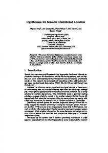
Figure 1: Pipelined QDI Full Adder Cell. are designed to make minimal timing assumptions.y Asynchronous active memory systems have architectural variations in access time that would be automatically handled by the QDI nature of their implementation. Pipelined QDI Asynchronous Circuits. A simple asynchronous pipeline stage can be described as a process that repeatedly receives an input data item, performs some computation on it, and transmits it to its environment. If we connect a number of such stages together, the result is a linear pipeline. The formal synthesis procedure introduced by Martin [17] transforms this simple process into QDI CMOS circuits using a sequence of semantics-preserving transformations. Figure 1 shows the result of the transformations applied to a full-adder speci cation. The adder receives three inputs on ports A, B , and C , and produces the sum on port S and the carry-out on port D .z There are several interesting features of this particular circuit implementation of a QDI pipeline stage: the input to output latency is two transitions, corresponding to low forward latency; the circuit can operate at very high throughput (in the range of 400MHz in a 0:6�m CMOS process); there are no timing margins necessary on the latency critical paths because of the QDI nature of the circuit. This QDI pipeline stage can be extended to construct more complex asynchronous systems, including interleaved memory systems, iterative structures, and other pipelining schemes [14]. The Making the relative timing assumptions present in QDI circuits leads to a completeness of the design technique [15]; without these assumptions, the class of correct circuits would be very limited [18]. z A variation of this circuit style was rst introduced by Williams [27]. y
AAM: ISCA 2000 Memory Wall Workshop
3
key to attaining high throughput in variable latency asynchronous pipelines is an analysis of the system based on the concept of dynamic wavelength [27], and slack matching [4].
Exploiting Average-Case Performance. In a clocked system, the global clock frequency is
determined by the maximum worst-case delay of all components in the system. Increasing the latency in any pipe stage can impact global performance through a lower clock rate. In an asynchronous system, a local latency increase would only a�ect the delay of the particular operation under consideration|and only when the operation is performed. We can exploit this tradeo� to improve the common-case performance of asynchronous memory systems. As a case in point, the MiniMIPS processor exploits average-case behavior to improve the performance of its on-chip memory system. The asynchronous cache organization in the processor has higher throughput than the individual memory banks, but a poor access pattern can result in a loss of throughput. However, unlike memory bank controllers in clocked processors [29], the MiniMIPS does not need any additional circuitry to detect these special access patterns, thereby simplifying the design. Accommodating these high-latency accesses has no impact on the latency of common-case fast access because the interface is asynchronous. The clocked approach would have to either stretch the global clock to accommodate the high-latency operation, or introduce an architectural pipeline bubble, further complicating the memory interface. In the rest of this section, we present our preliminary asynchronous memory architecture.
A Case For Asynchronous Mesh Memory. We are designing a prototype asynchronous mem-
ory system that uses point-to-point high-speed links to connect multiple memory elements using a scalable mesh interconnect, as shown in Figure 2. Such an architecture has several advantages over traditional bus-based memory systems. The point-to-point nature of the interconnect makes high-speed signaling protocols feasible [5,28], reducing overall memory access time and improving throughput. While bus-based systems are simpler to build because they serialize transactions to all memory banks, it is precisely this property that reduces their overall performance. Also, multiple senders and receivers on the shared bus wires a�ect electrical properties of the signaling protocol, reducing signaling rate. For example, the SGI Origin 2000 uses point-to-point links in its 2-processor nodes instead of a snoopy bus. Its point-to-point links make cache coherence more di�cult because of the lack of a broadcast mechanism, but the complexity increase was worthwhile because it reduced the common case memory access latency [13]. The problem with mesh-based memory systems is that they introduce complex non-uniform memory access latencies even within a uniprocessor . Accommodating these non-uniform access latencies in traditional clocked memory controllers would signi cantly increase their complexity [6]. Non-uniform memory latency does not increase the complexity of an asynchronous controller because its underlying circuit implementation is insensitive to delay variations. Our scalable asynchronous mesh-based memory architecture consists of two main components: a pipelined asynchronous multi-banked DRAM for high-density memory storage, and a router with dispatch logic to handle external memory requests. As far as the asynchronous memory controller is concerned, our asynchronous mesh memory simply accepts an address request and a simple command (like read or write), and returns data. AAM: ISCA 2000 Memory Wall Workshop
4
MULTI-BANKED DRAM ARRAY
ROUTER/DISPATCH memory controller
Figure 2: Asynchronous Mesh Memory. Accommodating Clocks: The Synchronous/Asynchronous Boundary. Until modern pro-
cessors are designed without clocks, a key challenge to making pipelined asynchronous memory operate e�ciently within a clocked system is transferring information from the asynchronous domain into the clocked domain. The problem arises when the asynchronous input arrives near a clock edge and violates setup/hold time constraints for the clocked interface, potentially causing the system to enter a metastable state [3]. Careful circuit design techniques can virtually eliminate the possibility of entering a metastable state. The problem with most of these techniques (stretchable clocks, multiple latches, multi-stage sampling, etc.) is that they reduce the data transfer throughput at the boundary in addition to introducing latency. Pipeline synchronization is a promising technique that keeps the data transfer throughput between the asynchronous and clocked domains high [25]. This technique introduces an asynchronous resynchronizing FIFO that gradually resynchronizes the asynchronous input to the clock, and is currently used by Myricom for their high-speed Myrinet network. While this technique keeps the throughput high, it still adds latency to the data transfer when crossing the boundary between the asynchronous and clocked domains. We are working on techniques that extend pipeline synchronization by merging the resynchronizing FIFO with other logical functions performed by the asynchronous portion of the memory controller to hide the resynchronization latency.
3. Asynchronous Active Memories Many researchers have proposed schemes for active memories|performing computation in the memory system itself|but in each case a nagging question is how these active memories, with inherently longer access times than normal memories, t into a conventional uniprocessor memory system. In Section 2 we explained how pipelined asynchronous memory systems naturally tolerate variations in memory access time without compromising performance in the common case. This is the critical feature that allows active memory processing elements to co-exist with conventional, inactive memory elements. Given an asynchronous mesh memory system, we propose to design a programmable asynchronous active memory element , that can function either as a normal meshconnected memory element or as an active memory element that processes data as it moves between memory and the main processor. AAM: ISCA 2000 Memory Wall Workshop
5
The target applications for active memories are those that exhibit poor cache behavior in traditional systems, either because of bad stride problems (e.g. vector codes, variable precision computation, or matrix transposes) or capacity constraints (e.g. out-of-core applications or searching large datasets). Our active memory element will support a set of operations that includes internal read-modify-write operations, where the modify step can be programmable, and a set of scatter/gather operations where the memory element can funnel data into or out of a base memory location with programmable stride. bcopy is a special-case of the read-modify-write operation where the modify component is the identity function. In-memory matrix transposes can be performed with a gathering read with stride equal to the row size of the matrix. That data may either be returned to the main processor or copied to another location within the memory element. In addition to support for read-modify-write and scatter/gather, the active memory element can also perform ltering operations that can reduce the amount of data transferred between the memory system and the main processor.
Address Remapping. Recent active memory proposals have advocated the technique of remap-
ping the address space of a process in an application-speci c manner and using accesses to this space as a signal to the memory controller to perform \active" operations rather than satisfying this access from physical memory [2,9]. For example, when performing matrix operations that require row and column traversals, one traversal uses the cache e�ectively whereas the other does not. We can provide multiple memory viewpoints of the same matrix using shadow address spaces much like that proposed in the Impulse memory controller [2] and for user-level messaging in the FLASH multiprocessor [9]. Row traversals would be unchanged, whereas column traversals would be treated as row traversals of a matrix at a di�erent (shadow) address. The memory controller would issue scatter/gather commands to the active memory elements which in turn would fetch individual double-words from a column and return them in a single cache line, thereby providing data in blocks that can be cached e�ciently by the main processor. The result would be good cache behavior for both row and column traversals of the matrix. Such an active matrix approach could potentially speed up many scienti c applications by using the processing capability in the memory system. Application developers could be presented with a set of Active matrix libraries analogous to existing libraries for performing linear algebra operations on parallel architectures (such as ScaLAPACK [1]).
Cache Coherence. The key challenge with active memory systems is solving the cache coherence
problem it creates. If columns of a matrix are being written via a di�erent address space during column traversals, what happens when the application reads from the normal row address during the next row traversal? The answer is that unless care is taken, the next row traversal will return incorrect or stale data. The key insight into solving the coherence problem in active memory systems is that the active memory controller that controls the coherence protocol also controls the active memory elements. In architectures like the Stanford FLASH multiprocessor [12] the coherence protocol itself is also programmable. Thus, it is possible to combine the coherence protocol and active memory support and treat active memory as an extension of the cache coherence protocol. AAM: ISCA 2000 Memory Wall Workshop
6
data-intensive tasks performed in parallel by active memory elements
active memory controller
cache coherence protocols
Processor
host processor
$
Figure 3: Two-level Active Memory System. Two-level Active Memory Systems. We make the distinction between active memory con-
trollers and active memory elements. The MAGIC node controller in the Stanford FLASH multiprocessor can be viewed as an active memory controller because its programmable protocol processor handles every access to the memory system. While the FLASH multiprocessor has an active memory controller, it uses standard SDRAM parts rather than active memory elements. Our initial work with active memory controllers using the FLASH prototype indicates that the occupancy of the active memory controller would be signi cantly reduced by the introduction of active memory elements, thereby improving overall system performance [11]. We introduce a two-level approach to active memory systems that focuses on designing asynchronous active memory elements that can assist an active controller in performing data-intensive operations in the memory system itself. While the data-intensive calculations are best performed in the active memory element, the cache coherence problem is best solved in the active memory controller. This novel two-level approach to active memory systems is depicted in Figure 3. Our active memory elements are easily integrated into the asynchronous mesh architecture proposed in Section 2 by an extension of the memory interface read/write commands. For example, non-active references remain traditional read and write operations to the memory element, while scatter/gather operations require only an additional stride. An asynchronous active memory system can tolerate the additional latency of these more complex active memory operations without any specialized support, making them an ideal framework for exploring the e�cacy of active memory systems.
4. Conclusions and Future Work Our proposed research on asynchronous active memories provides a novel platform for studying AAM: ISCA 2000 Memory Wall Workshop
7
issues in both high-performance traditional memory systems as well as active memory systems. In particular, our pipelined asynchronous approach sees the following bene ts: � Simpler Controller Design. Our design uses recently developed techniques in modern pipelined asynchronous design, alleviating the timing constraints present in conventional clocked memories while providing higher sustained throughput and the innate ability to handle variations in memory access time. � Average-Case Performance. In an asynchronous system, a local latency increase only a�ects the delay of the particular operation under consideration|and only when the operation is performed. We can exploit this tradeo� to improve the common-case performance of asynchronous memory systems. � Non-Uniform Memory Access. The inherent ability of asynchronous memory controllers to tolerate variable access latencies permits the design of scalable asynchronous mesh memories. Although the mesh structure creates a non-uniform access time, the overall memory bandwidth is higher and accesses can potentially be faster by exploiting average case performance. � Transparent Support for Active Memories. The drawback of active memories has long been their inability to be incorporated into a standard memory system because an \active" access can involve a non-trivial amount of computation and result in a much longer access time than a normal memory access. An asynchronous active memory system can tolerate the additional latency of these more complex active memory operations without any specialized support. We believe these bene ts of asynchronous active memory systems have the potential to lower the memory wall in modern processors and provide a framework for the ongoing study of scalable high-performance memory systems.
References
[1] L. S. Blackford, J. Choi, A. Cleary, E. D'Azevedo, J. Demmel, I. Dhillon, J. Dongarra, S. Hammarling, G. Henry, A. Petitet, K. Stanley, D. Walker, and R. C. Whaley. ScaLAPACK: A Linear Algebra Library for Message-Passing Computers. SIAM Conference on Parallel Processing , March 1997. [2] J.B. Carter, W.C. Hsieh, L.B. Stroller, et al. Impulse: Building a Smarter Memory Controller. In Proceedings of the Fifth International Symposium on High Performance Computer Architecture January 1999. [3] T.J. Chancey and C.E. Molnar. Anomalous Behavior of Synchronizer and Arbiter Circuits. IEEE Transactions on Computers , 22(4):421{422, April 1973. [4] Uri V. Cummings, Andrew M. Lines, and Alain J. Martin. An asynchronous pipelined lattice-structure lter. In Proceedings of the First International Symposium on Advanced Research in Asynchronous Circuits and Systems , pp. 126{133, November 1994. [5] W.J. Dally and J. Poulton. Equalized 4Gb/s Signalling. In Hot Interconnects IV Symposium Record , September 1996.
AAM: ISCA 2000 Memory Wall Workshop
8
[6] Direct Rambus Memory Controller Speci cation. Accessible from http://www.rambus.com/. [7] Maya Gokhale, Bill Holmes, and Ken Iobst. Processing in Memory: the Terasys Massively Parallel PIM Array. Computer , 28(3):23{31, April 1995. [8] M. Hall et al. Mapping Irregular Applications to DIVA, A PIM-based Data-Intensive Architecture. Supercomputing , Portland, OR, Nov. 1999. [9] J. Heinlein. Optimized Multiprocessor Communication and Synchronization Using a Programmable Protocol Engine . Ph.D. Dissertation, Stanford University, Stanford, CA, March 1998. [10] J. Hennessy and D. Patterson. Computer Architecture: A Quantitative Approach. 2nd Edition, Morgan Kaufmann, San Francisco, CA, 1996. [11] C. Holt, M. Heinrich, J. P. Singh, et al. The E�ects of Latency, Occupancy, and Bandwidth in Distributed Shared Memory Multiprocessors. Technical Report CSL-TR-95-660, Computer Systems Laboratory, Stanford University, January 1995. [12] J. Kuskin, D. Ofelt, M. Heinrich, et al. The Stanford FLASH Multiprocessor. In Proceedings of the 21st International Symposium on Computer Architecture , pages 302-313, April 1994. [13] J. Laudon and D. Lenoski. The SGI Origin: A ccNUMA Highly Scalable Server. In Proceedings of the 24th International Symposium on Computer Architecture , pages 241{251, June 1997. [14] Andrew M. Lines. Pipelined Asynchronous Circuits. M.S. Thesis, California Institute of Technology, 1996. [15] Rajit Manohar and Alain J. Martin. Quasi-delay-insensitive circuits are Turing-complete. Invited article, Second International Symposium on Advanced Research in Asynchronous Circuits and Systems , March 1996. Available as Caltech technical report CS-TR-95-11, November 1995. [16] Rajit Manohar, Tak-Kwan Lee, and Alain J. Martin. Projection: A Synthesis Technique for Concurrent Systems. Proceedings of the Fifth International Symposium on Advanced Research in Asynchronous Circuits and Systems , April 1999. [17] Alain J. Martin. Compiling Communicating Processes into Delay-insensitive VLSI circuits. Distributed Computing, 1(4), 1986. [18] Alain J. Martin. The limitations to delay-insensitivity in asynchronous circuits. Sixth MIT Conference on Advanced Research in VLSI , 1990 [19] Alain J. Martin, Steven M. Burns, Tak-Kwan Lee, Drazen Borkovic, and Pieter J. Hazewindus. The design of an asynchronous microprocessor. In Charles L. Seitz, editor, Advanced Research in VLSI: Proceedings of the Decennial Caltech Conference on VLSI , pp. 351{373, MIT Press, 1991. [20] A. J. Martin, A. Lines, R. Manohar, et al. The Design of an Asynchronous MIPS R3000. In Proceedings of the 17th Conference on Advanced Research in VLSI , pages 164{181, September 1997. [21] M. Oskin, F.T. Chong, and T. Sherwood. Active Pages: A Computation Model for Intelligent Memory. In Proceedings of the 25th International Symposium on Computer Architecture , 1998. [22] D.A. Patterson, T. Anderson, et al. A Case for Intelligent RAM: IRAM. IEEE Micro , 17(2), April 1997. [23] S.A. Perl and R.L. Sites. Studies of Windows NT Performance using Dynamic Execution Traces . Digital SRC Research Report 146, April 1997. [24] A. Saulsbury, F. Pong, and A. Nowatzyk. Missing the Memory Wall: The Case for Processor/Memory Integration. In Proceedings of the 23rd International Symposium on Computer Architecture , pages 90101, May 1996. AAM: ISCA 2000 Memory Wall Workshop
9
[25] Jakov N. Seizovic. Pipeline Synchronization. In Proceedings of the First International Symposium on Advanced Research in Asynchronous Circuits and Systems , pages 87-96, November 1994. [26] Stephen Shankland. Intel to delay new chipset as Rambus reels. CNET News.com, September 24, 1999. [27] Ted Eugene Williams. Self-timed Rings and their Application to Division . Ph.D. thesis, Computer Systems Laboratory, Stanford University, May 1991. [28] C.K. Yang and M.A. Horowitz. A 0.8mm CMOS 2.5Gb/s Oversampled Receiver for Serial Links. IEEE International Solid-State Circuits Conference, Digest of Technical Papers , February 1996. [29] Ken Yeager. The MIPS R10000 Superscalar Microprocessor. IEEE Micro , 16(2):28{40, April 1996.
AAM: ISCA 2000 Memory Wall Workshop
10