Important Properties of Transient Thermal Impedance for MOS–gated Power Semiconductors Željko Jakopović, Zvonko Benčić, Fetah Kolonić University of Zagreb Faculty of Electrical Engineering and Computing Unska 3, HR-10000 Zagreb, Croatia
[email protected],
[email protected],
[email protected] Abstract – Important properties of transient thermal impedance (TTI) for MOS-gated power semiconductors are investigated on the base of measurement results. Electrical method of transient thermal impedance measurement was used with different temperature sensitive electrical parameters (TSEPs). A wide variety of measurements on MOSFET and IGBT samples was performed, to be able to answer on the questions about TTI existance conditions. Different types of temperature responses were used , as well as different power dissipation levels and conditions. Final TEMPFET test, with simulation and measurement of overtemperature protection reaction time, shows that TTI of MOS-gated components, if properly measured, can be successfully used for simulative estimation of semiconductor’s operating temperature.
I. INTRODUCTION Transient thermal impedance Zth(t) was defined by Diebold and Luft [1] in 1961. as time response of temperature diference between silicon temperature and reference point (TJ(t)-TRef(t)) caused by constant power dissipation pulse P. Usually, transient thermal impedance of power semicondutor is represented with transient thermal impedance curve (TTIC), and published in catalogues. At the first time after definition, transient thermal impedance was calculated analiticaly, or measured with not so accurate methods. Lately, more precise measurement methods are developed, as well as sophisticated modelling tools. Transient thermal impedance is used for the calculation of silicon’s temperature rise (static od dynamic) because of power dissipation developed in power semiconductor. Different methods are applied for that purpose, grapho-analytical, analytical and numerical. To be properly used for the calculation of silicon’s temperature rise, transient thermal impedance and thermal system which is representing, should fulfill some conditions, named existance conditions. Thermal system for which TTIC is defined should be linear, time invariant, with time invariant space distribution of power dissipation. TTIC measurement method (mainly electrical) and used thermo-sensitive electrical parameter are also important for accuracy of results. It is natural that all required properties are not 100% fulfilled, but it is interesting to explore in what extent are fulfiled properties of TTIC, answering the needs for accurate calculation of semiconductor’s silicon temperature. This topic is not enough analyzed and described in literature, just few papers are dealing with that problem [4]. In power semiconductor catalogues, just TTIC is given, with no description of it’s measurement
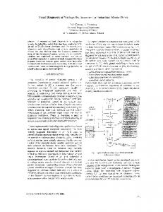
conditions. At present time, some sophisticated electrothermal models of power semiconductors are developed [6], but they are not yet available for wide use, as standard procedure. The purpose of the paper is to prove that power semiconductor’s TTIC can be used for accurate calculation of silicon temperature in real operating conditions. Important properties of semiconductor’s thermal system and transient thermal impedance are examined by measurement under different conditions. Obtained results are then analyzed, giving the answer on the question of transient thermal impedance existance conditions, what is important for it’s application for silicon’s temperature calculation. Finally, it is proven on the TEMPFET example, that TTIC can be used with sufficient accuracy for the calculation of silicon’s temperature. II. MEASUREMENT SYSTEM AND METHODS Electrical method of transient thermal impedance measurement was used, with different temperature sensitive electrical parameters (TSEPs). As examined power semiconductor devices, MOSFETs and IGBTs in TO-220 and TO-247 cases were used. Measurement system was computer controlled and universal [3,5,7], for different TSEPs, different measurement methods and different types of power dissipation. Power part of measurement system (Fig.1.) contains device under test (DUT), auxiliary switch (S) and dummy load (DL). The heart of measurement system is switching device (Fig.2) consisting of logical part, control part and power part. Additional instruments were used to build transient thermal impedance measurement system, waveform generators, digital oscilloscope and highly accurate digital multimeter (HP3458A). A. Temperature sensitive electrical parameters Different temperature sensitive electrical parameters are appropriate for measurement of silicon’s temperature. MOSFET has 3 appropriate TSEPs, threshold voltage (VT), voltage drop on integral diode (VSD) and on-state resistance (RDSon). IGBT has only 2 appropriate TSEPs, threshold voltage (VT) and collector-emmiter voltage drop (VCES). Before transient thermal impedance measurement, thermal callibration of TSEPs has to be provided, to obtain their temperature dependance. B. Types of temperature responses
Transient thermal impedance (in fact, temperature response) can be measured during semiconductor’s heating phase - heating response (ZthH), or during semiconductor’s S DL
U B
III. ANALYSIS OF MEASUREMENT RESULTS DUT
IM
A. Temperature sensitive electrical parameters
Fig. 1. Power part of TTIC measurement system.
CONTROL SIGNAL
switching losses). Linearity of thermal system is fulfilled if all types of losses with same level are resulting with the same temperature rise. If this is not true, the worst case should be indicated, giving the greatest temperature rise. Transient thermal impedance should be measured under this, worst conditions, to give conservative results in application.
CONTROL PART
LOGICAL PART SELECTING OPERATING MODUS
HEATING CURRENT AND POWER CONTROL
CONTROL SIGNAL PROCESSING
HEATING CURRENT AND POWER SETTING
DELAY
DELAY CIRCUITS
I
H
ACTUAL HEATING CURRENT MEASUREMENT
HEATING CURRENT MEASUREMENT
CONTROL SIGNALS FOR ALL SWITCHES
POWER PART TSEP MEASUREMENT
DUT (MOSFET / IGBT) AUX. SWITCH - S (MOSFET) DUMMY LOAD - DL (MOSFET)
PASSIVE COMPONENTS CONTROL MEASUREMENT OF V AND I
VOLTAGE AND CURRENT SOURCES
Fig. 2. Switching device – the heart of the TTIC measurement system.
cooling phase - cooling response (ZthC). Heating response is much more complicate to measure than cooling response. For ideal, linear thermal system, heating and cooling temperature responses should be complementary. Fulfillment of this condition should lead to simplification of measurement procedure, as well as to possible application of linear electrical model of power semiconductor’s thermal system. C. Power dissipation levels and conditions For ideal thermal system, linearity property exists. That means, double the dissipation, double the temperature rise. To investigate the linearity property of power semiconductor’s thermal system, transient thermal impedance was measured under different levels of power dissipation, from 20% of maximum allowed dissipation PM to 500% (short pulse) of PM. It is also important to investigate if different combinations of current and voltage, giving the same power dissipation (PH = IH * UH), are resulting with the same temperature rise. For bipolar power transistors this is not true [2]. D. Power dissipation types Power dissipated in power semiconductor can be developed in static regimes (full conduction/saturation or active region of VI characteristic) or in dynamic regimes (combined losses consisting of conduction losses and
Different TSEPs are temperature indicators of different regions of semiconductor devices. As expected, for the same power dissipation PH, temperature measured with different TSEPs as temperature indicators, resulted with different measured silicon temperatures. The greatest temperature gives threshold voltage VT, in MOSFET and IGBT case. Threshold voltage is temperature indicator of surface and channel region of semiconductor device. Lower temperature gives diode voltage drop VSD at MOSFET and VCES at IGBT. The lowest temperature was indicated by on-state resistance RDSon in MOSFET case. It is not easy to decide which TSEP to use as temperature indicator in transient thermal impedance measurement. Of course, threshold voltage gives surely the temperature nearest to the maximum silicon temperature measured with optical methods (IR microradiometer), measurement method is relatively simple, but threshold voltage temperature characteristics are not so unique, that means that VT is not appropriate for large series measurement. Fig.3. gives an illustration of the influence of chosen TSEP on resulting transient thermal impedance curve. B. Types of temperature responses Agreement between the measured heating and cooling responses was surprisingly well. With only small number of exceptions (measurement near the limits of dissipation PH), excellent or very good agreement between ZthH and ZthC was measured, indicating that in the normal operating temperature range (25°C-125°C), MOSFET’s and IGBT’s thermal systems are quite linear. That means that it’s transient thermal impedance curve can be successfully measured during cooling phase, what is much simpler to realize than measurement during heating phase. As an illustration of relatively good agreement between heating and cooling response, Fig.4. can serve. Cases with total agreement between heating and cooling response are senseless to show, because just one curve can be seen. C. Power dissipation levels and conditions It is hard to unify the results of transient thermal impedance measurements under different dissipation levels and heating current levels. It seems that different factors are interconnected, so that there is no unique answer for the behavior of TTIC for observed conditions. The good side of the problem is that the scattering of measured TTIC is relatively small, except in the case of reaching maximum junction temperature, meaning that the worst case transient thermal impedance curve can lead to
accurate thermal model of semiconductor device for silicon’s temperature calculation. Fig.5. gives an illustration of the power dissipation level influence on the transient thermal impedance.
TSEP - VT TSEP - VSD
Fig. 6. Comparison of measured TTICs for different types of dissipation PH
Agreement between the measured TTICs is good until the silicons’s temperature reaches approximately 150°C, as indicated in the case of PH=120 W. It seems that during that high temperature rise, current is crowding through smaller area than at normal silicon’s temperatures. This fact is valid for MOSFET as well as for IGBT. It is not advisable to measure the TTIC at small levels of dissipation (e.g.10-20% of PM), because of larger measurement error. So the proposal is to measure the TTIC at approximatelly 50% of semiconductor’s PM.
TSEP - RDSon
D. Power dissipation types Fig. 3. Comparison of measured TTIC for MOSFET, based on different TSEPs.
C O O L IN G R E S PO N S E H E A T IN G R E S P O N S E
Fig. 4. Comparison of measured heating and cooling responses (ZthH, ZthC)
For practical application of TTIC for silicon’s temperature calculation in the real operating conditions, it is important to know the dependance of TTIC on the different types of dissipation. Developed measurement system for transient thermal impedance measurement enables temperature (and thus TTIC) measurement under wide spectrum of semiconductor’s operating regimes. Saturation (full conduction) and active region were analyzed during static measurement, as well as combined losses (conduction and switching losses) similar or equal to real operating condition losses during dynamic measurement. The ratio between conduction and switching losses was changeable. Results are very interesting. The field of measured TTICs was obtained. Lower boundary (smallest Zth) curve was measured during heating phase in saturation mode and upper boundary (largest Zth) was measured during heating phase in the worst case active region (small heating current IH, large voltage VH). All possible TTICs measured during heating with combined losses ware placed between this boundary curves. This fact is very important for practical use of TTIC. The TTIC should always be measured in active operating region of semiconductor device, what ensures conservative results in calculation of silicon’s temperature in the real operating conditions. Fig.6. illustrates the described facts on the IGBT example. IV. APPLICATION OF TRANSIENT THERMAL IMPEDANCE
Fig. 5. Comparison of measured TTIC for different levels of dissipation PH
SATURATION, P = 38 W f = 25 kHz, P = 45 W, COMB. f = 100 kHz, P = 42 W, COMB. f = 100 kHz, P = 18 W, COMB. ACTIVE REGION, P = 40 W
From the analysis of transient thermal impedance properties it can be concluded that for MOSFETs and IGBTs it can be succesfully used in calculation of silicon’s temperature with simulative methods. But this thesis needs the verification. An idea is to use independent temperature indicator, not the one used for TTIC measurement, and to compare the results of temperature measurement and simulation for the same operating cyclus of semiconductor device. The method is described in details in [8], in this paper only the basic facts are emphasized. As temperature indicator, TEMPFET was used, MOSFET with integrated overtemperature protection. Before the use, TEMPFET was calibrated to find out it’s overtemperature protection reaction temperature. This critical temperature Tcrit, was find out repeatable and very stable (Tcrit = 170°C at TAMB = 17°C). Also the TTIC for the device was measured. TTIC was measured with
threshold voltage as TSEP and in active operation region during heating phase. This should give the worst case
u S (5 V/div)
iS (4 A/div) 0 – uS PS (80 W/div)
0 – iS , PS t – 1 0 ms/div
TTIC for examined TEMPFET. On the base of measured Fig. 7. Measurement of overtemperature protection reaction time for losses generated in active region of operation (PS(AV) = 223 W)
Δ T(K, 20K /di v.) Δ TJ ΔTS
the simple thermal model with parameters extracted from the measured TTIC is accurate enough to be used in practice. Fig.7. and 8. are illustrating the idea of verification procedure, comparing the results of overtemperature protection measurement and simulation. In observed case, amplitude of applied active region losses was PH=223 W, resulting with overtemperature protection reaction time of 35.4 ms. Simulation of the sensor’s temperature TS(t) (not junction–silicon temperature!) gives protection reaction time of 32 ms. The difference between the results could be caused by the inaccuracy of the TEMPFET’s thermal model, where thermal system of sensor was implemented in the simplest way [8]. Table I presents the comparative results of all the measured data with simulated data. Measured protection reaction time tRM is in an excellent agreement with simulated reaction time tRSSM based on the sensor temperature TS and measured transient thermal impedance curve. The agreement between the results would surely be even better if the TEMPFET's structure was better described in thermal model. If the simulation of reaction time tRSJM is based on the silicon temperature TJ (not taking into account temperature sensor thermal circuit) the agreement between the results is not so good, especially for shorter protection reaction times. The simulation based on the catalogue data for transient thermal impedance (not self–measured) gives much worser agreement between the measured tRM and simulated tRSJK reaction times showing that catalogue data are too conservative in this case. For lower dissipation levels (PS = 78 W), simulation based on catalog TTIC data showed no overtemperature protection reaction. The reason for that fact is primary in the influence of contact thermal resistance between the case and the heatsink, which was not taken into account in this case. TABLE I COMPARISON OF MEASURED AND SIMULATED RESULTS OF OVERTEMPERATURE PROTECTION REACTION TIME (TR)
t RSJM
t R SSM t (ms) tRM
Fig. 8. Simulation of overtemperature protection reaction time for losses generated in active region of operation (PS(AV) = 223 W)
TTIC, appropriate thermal model of TEMPFET was build, as a simple, modified ladder RC model [8], with parameters identified on the base of it’s TTIC. Electrothermal model was implemented into SIMPLORER, powerful simulation package for power electronics systems. As power dissipation source PH, measured TEMPFET’s voltages and currents (with calculated power) were used, ensuring the same conditions for simulation and measurement. TEMPFET was forced to reach the critical temperature Tcrit, when it’s overtemperature protection reacts. Several types of dissipation were used, from short circuit to combined losses. Time for overtemperature protection to react was measured and simulated. A very good agreement between the measured and simulated protection reaction time was find out, meaning that the procedure for simulative calculation of silicon’s temperature based on
tRSSM tRSJM tRSJK
COMBINED P = 78 W
ACTIVE MODE P = 78 W
ACTIVE MODE P=118 W
ACTIVE MODE P=223 W
ACTIVE MODE P=332 W
560 ms
530 ms
170 ms
35,8 ms
15,4 ms
495 ms
500 ms
156 ms
32 ms
19 ms
450 ms
480 ms
140 ms
12,6 ms
4,4 ms
*
*
23 ms
3,3 ms
1,2 ms
IV. CONCLUSION Important properties of transient thermal impedance, named existance conditions, for MOS-gated power devices (MOSFETs and IGBTs) were examined. Universal measurement system was developed, enabling wide spectrum of measurement methods and conditions. Results of measurement are showing that at MOS-gated power devices, existance conditions of transient thermal impedance, basically linearity of semiconductor thermal system, are fulfilled enough to enable succesful and accurate enough application of transient thermal
impedance for simulative calculation of silicon’s temperature in the real operating conditions. Simulation can be based on the simple thermal model of power semiconductor. Final verification was provided on the TEMPFET example, when overtemperature reaction time was measured and simulated for the same conditions. Good agreement of measured and simulated results confirms the expectations. For practical application of TTIC for estimation of semiconductor’s temperature, TTIC should be properly measured (with appropriate TSEP and method). Experiences with today’s catalogue data are not satisfactory. V. ACKNOWLEDGMENT The authors gratefully acknowledge the contributions of SIMEC Gmbh. They helped us by ensuring latest version of SIMPLORER® simulation package, needed for successful electro-thermal simulation.
REFERENCES [l] [2] [3] [4] [5] [6] [7] [8]
Diebold E.J., Luft W., “Transient Thermal Impedance of Semiconductor Devices”, AIEE Trans., pp.719-726, 1961. Rubin S., Oettinger F.F.,”Thermal Resistance Measurements on Power Transistors”, NBS Publication, pp.400-414., 1979. Blackburn D.L., Berning D.W.,”Power MOSFET Temperature Measurement”, PESC’82 Proceedings, pp.400-407, 1982. Siegal B.S.,”Factors Affecting Semiconductor Device Thermal Resistance Measurements”, SEMI-THERM 4 Proceedings, pp.1218., San Diego, 1988. Jakopovic Z.,”Computer Controlled Measurement of Power MOSFET Transient Thermal Response”, PESC’92 Proceedengs, pp.1026-1032., Toledo, Spain, 1992. Hefner A.R.Jr.,”A Dynamic Electro-Thermal Model for the IGBT”, IEEE Trans.on Ind.Appl., Vol.30, No.2.,pp.394-405, 1994. Jakopovic Z., “Application Limits of Transient Thermal Impedance for MOS-gated Semiconductor Devices”, PhD Thesis, University of Zagreb, Croatia, 1997. (in Croatian) Jakopovic Z., Kolonic F., Bencic Z., “The Estimation of Semiconductor’s Silicon Temperature in the Real Operating Conditions”, PEMC’98 Proceedings, pp.1.17.-1.21., Prague, 1998.