Automation for Partial Reconfiguration (DAPR) PR design flow. The DAPR design flow ... provided bus macro placement âbest practicesâ can produce designs with suboptimal ...... [12] S. M. Sait and H. Youssef, âVLSI Physical Design Automation: Theory and Practiceâ, World Scientific Publishing Company, 1st edition, 1999.
DAPR: Design Automation for Partially Reconfigurable FPGAs Shaon Yousuf and Ann Gordon-Ross NSF Center for High-Performance Reconfigurable Computing (CHREC) Department of Electrical and Computer Engineering, University of Florida, Gainesville, FL 32611 {yousuf, ann}@chrec.org Abstract—Partial reconfiguration (PR) enhances traditional FPGA-based high-performance reconfigurable computing by providing additional benefits such as reduced area and memory requirements, increased performance, and increased functionality. However, since leveraging these additional benefits requires specific designer expertise, which increases design time, PR has not yet gained widespread usage. Even though Xilinx’s PR design flow significantly eases PR design, to fully leverage PR benefits designers require extensive PR design flow knowledge, as well as low-level architectural details of the target FPGA device. In this paper, we present a PR design flow and associated tool to automate PR design intricacies and design space exploration. Our design flow and tool can significantly reduce PR design time effort and make PR designs more accessible and amenable to a wider range of PR designers.
I. INTRODUCTION AND MOTIVATION Dynamic reconfiguration in SRAM-based FPGAs is an extremely beneficial feature for high-performance embedded designs. By dynamically reconfiguring FPGA configuration memory with various design specifications (bitstreams), hardware functionality can time-multiplex FPGA resources. The dynamic reconfiguration method affects the bitstream format. Full bitstreams, used for full reconfiguration (FR), contain configuration information for the entire FPGA. Partial bitstreams, used for partial reconfiguration (PR), contain configuration information for a portion of the FPGA. FR and PR expand FPGA resources to nearly an infinite amount, resulting in reduced total resource requirements and increased flexibility through on-demand design specification loading/unloading. Additionally, since FR and PR can potentially decrease the number of required devices or device size, FPGA power consumption can also be reduced [10]. However, dynamic reconfiguration has several drawbacks. Since FR requires reconfiguring the entire FPGA even for small design changes, memory resources are wasted as multiple large full bitstreams containing redundant configuration information need to be stored. Additionally, FR interrupts design execution during FPGA reconfiguration. This interruption or reconfiguration time can impose unacceptable performance overheads, especially for real-time systems. Alternatively, PR mitigates FR’s drawbacks by isolating reconfiguration to a portion of the FPGA while all other remaining FPGA resources continue execution [11]. PR designs partition the FPGA into a static region and several individually reconfigurable PR regions (PRRs). The static region implements a PR design’s base functionality
and is never reconfigured, while the PRRs are loaded/unloaded on demand with PR modules (PRMs). A PRM constitutes a portion of a PR design’s functionality. Since PR isolates the static region and PRRs, PR reduces memory requirements by eliminating the need for multiple full bitstreams containing redundant configuration information. PR designs require only one full bitstream to initialize a PR design’s initial static region and PRRs. During execution, different PRM partial bitstreams can be loaded into the PRRs on demand. Additionally, since partial bitstreams are significantly smaller than full bitstreams, PR reconfiguration time is faster than FR reconfiguration time [9]. PR is particularly useful for designs that do not simultaneously require all their functionality and can benefit from uninterrupted reconfiguration (SDRs [10], JPEG [16]). Despite PR’s enhancements over FR, PR designs have several drawbacks. PR designs are primarily supported by Xilinx’s Early-Access (EA) PR design flow [14], which requires manual intervention and significant design time effort. In addition to defining a PR design’s functionality and partitioning the design into the PRMs, PR designers must perform PR-specific tasks such as instantiating bus macro [14] VHDL specifications. Thus, even with Xilinx’s EA PR design flow, realizing PR benefits is challenging as lack of sufficient expertise can result in poor design performance. Currently, there exists little support for PR designers, and, to the best of our knowledge, there exists no previous efforts to completely automate the EA PR design flow’s design space exploration. In this paper we present the Design Automation for Partial Reconfiguration (DAPR) PR design flow. The DAPR design flow reduces PR design time effort and complexity, allowing rapid PR design prototyping and making PR more amenable to a larger range of designers.
Figure 1: Xilinx's EA PR design flow (left side) and the DAPR design flow (right side).
II. BACKGROUND AND RELATED WORK A. Xilinx’s EA PR Design Flow Figure 1 (left side) depicts Xilinx’s EA PR design flow [14]. The EA PR design flow requires a hierarchical logical partitioning of the VHDL design files into non-overlapping PRMs. Next, the designer must: (1) synthesize each design file separately; (2) create the PR design’s floorplan; (3) implement separate non-PR designs for every PRM to PRR combination and perform timing analysis on each design to verify timing requirements; (4) generate place and route information for the static region to create a static design with “holes” (un-placed and un-routed regions) for the PRMs and then generate place and route information for each respective hole’s (PRR’s) PRM; and (5) merge the static design’s place and route information with each PRM’s place and route information to generate the PR design’s multiple full and partial bitstreams. Each full bitstream contains configuration information for different PRM to PRR combinations allowing any startup PR design functionality and modifying the functionality with partial bitstreams during runtime. Xilinx ISE [14] utilities individually handle steps 1, 4, and 5 and Xilinx PlanAhead [14] aids step 2 (PR design floorplanning). Floorplanning defines area constraints (set in Xilinx’s user constraints file (.ucf)) that specify bus macro and resource placements as well as each PRR’s location and dimension (size and shape) on the FPGA. Although PlanAhead provides useful floorplanning information, there exists no formal process for determining optimal bus macro and PRR placements. Additionally, FPGA manufacturer provided bus macro placement “best practices” can produce designs with suboptimal design performance [3]. Bus macro floorplanning depends on the target device type. Xilinx Virtex-4 device bus macros are slice-based [14] and span the static region and PRR boundaries. Bus macros are Xilinx provided hardwired logical elements that lock wire routing between the static design and PRMs. All signals except global signals (e.g. clock signals) between the static design and PRMs must pass through bus macros to ensure communication between the static region and PRMs remains established during reconfiguration. PRR floorplanning
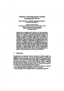
(a) (b) Figure 2: Virtex-4 LX25 (a) Virtex-4 LX25 FPGA resource layout with .dil file banks and (b) .dil to device floorplan mapping.
ensures PRRs encompass enough hardware resources to support the resource requirements of each PRM mapped to a PRR. Proper floorplanning ensures correct placement of both bus macros and PRRs but several correct placements exist and not all placements will result in the same design performance. For example, a PRR’s dimension can affect the maximum attainable clock frequency [5]. Figure 2 (a) depicts a Virtex-4 LX25 FPGA fabric and resource types including: configurable logic blocks (CLBs), block RAMs (BRAMs), first-in first-out buffers (FIFOs), digital signal processors (DSPs), digital clock managers (DCMs), input/output buffers (IOBs), and global buffers (BUFGs). CLBs, BRAMs, FIFOs, and DSPs are in the right and left halves of the fabric, whereas DCMs and BUFGs are in the center. CLBs consist of four slices and are the main logic resource used for sequential and combinatorial circuits.
B. Previous work Previous work proposes the special-purpose (SP) and multipurpose (MP) [5] PR design methodologies. The SP PR design flow creates custom PR designs tailored for a target system and the MP design flow creates generalized PR design templates for implementing a variety of systems. Since a critical design flow stage is PRR floorplanning, the authors proposed cost functions to evaluate PRR placement quality with respect to the PRR aspect ratio (PRR height in slices divided by PRR width), internal fragmentation, position relative to IOBs, and routability. Craven et al. [6] presented a high-level development environment for implementing dynamically reconfigurable hardware and used a simulated annealing based automated floorplanner and a BusMacroHelper tool for PRR and bus macro placement, respectively. No details were presented on the mechanism or effectiveness of the BusMacroHelper tool. Carver et al. [3] developed an automated simulated annealing-based bus macro placement tool and evaluated the tool using timing results generated by Xilinx’s PAR (place and route) utility. However, PRR dimensions were fixed and manually placed and timing evaluation was done for the static and PRM designs separately. Alternatively, DAPR automates PRR placement and evaluates the complete design’s timing and partial bitstream size using the final output bitstreams. Much previous work focuses on floorplanning techniques for reconfigurable designs [1][2][6]. Singhal et al. [13], Cheng et al. [4], and Feng et al. [8] used simulated annealing algorithms for automated PRR floorplanning, but these methods did not automate bus macro placement nor apply their floorplanning techniques to a PR design flow. Even though there exists much research on bus macro and PRR placement, to the best of our knowledge this is the first attempt to circumvent PR design flow burdens and complexities by automated design space exploration of both bus macro and PRR placement through the evaluation of PR design output bitstreams. Our work also aims to isolate designers from PR design low-level details and intricacies.
III. DAPR DESIGN FLOW The DAPR design flow reduces PR design time effort and complexities by automating many of Xilinx’s EA PR design flow’s difficult steps. Figure 1 depicts the DAPR design flow (right side) compared to Xilinx’s EA PR design flow (left side). The DAPR design flow is a generic, module-based reconfiguration PR design flow and uses vendor specific (Xilinx in this case) utilities to assist in bitstream generation. The DAPR design flow consists of a manual step and an automated step. In the manual step, the designer annotates the top-level VHDL design files and sets design constraints (optional). These annotations and design constraints serve as input to the automated step, which is orchestrated by the DAPR tool to automate the complex portions of Xilinx’s EA PR design flow. The DAPR design flow can be adapted to support different PR devices by updating how the vendor utilities are integrated in the DAPR tool. The DAPR tool works in four phases, which generate the PR design’s full and partial bitstreams. In this section, we describe the DAPR design flow steps and the DAPR tool phases.
A. DAPR Design Flow Steps In the DAPR design flow’s first manual step, the designer performs several straightforward tasks to prepare the PR design for the second automated step. First, the designer annotates the VHDL component instantiations in the toplevel design file using standard formatted VHDL comments (the designer must also follow Xilinx’s EA PR design VHDL formatting guidelines (Section II.A), which assumes that all PRR instantiations are defined in the top-level file). Using VHDL comments ensures that these annotations will not introduce synthesis errors or affect design portability. Optionally, the designer can define PR design constraints (e.g. timing, power, area, partial bitstream size, I/O primitive definitions, etc.) and the DAPR tool’s effort level control value (Section III.B) in a design constraints file (.dcs). After completion of the manual step, the DAPR tool’s
Figure 3: DAPR tool phases.
inputs are the annotated top-level design file, all other design files, and the .dcs file. The DAPR tool manipulates these files to generate the PR design’s full and partial bitstreams.
B. DAPR Tool Phases The DAPR design flow’s second automated step, depicted in Figure 3, consists of four phases. In phase 1, information identification uses the design file annotations to identify the static region and PRR instantiations, bus macro instantiations, and design file names. Information extraction extracts port map connection information from the region instantiations. The extracted connection information is written to a PR automation information file (.prai). Collectively, phases 2 through 4 iteratively generate candidate PR designs. Phase 2, the candidate generation phase, constitutes the bulk of DAPR’s work and automatically (1) synthesizes all design files using Xilinx’s XST utility, (2) estimates the hardware resource requirements from the generated synthesis log file (.srp) and records the requirements in the .prai file, (3) reads the port map connection information from the .prai file, generates a connectivity information file (.dot), and generates a connectivity graph for these regions, (4) uses the device information library file’s (.dil) estimated resources, connectivity information, and .ucf file to build an initial candidate floorplan if the .ucf file does not contain an existing floorplan, otherwise builds a new candidate floorplan, and (5) writes the current candidate floorplan constraints to a new .ucf file. The .dil file is currently generated in-house as part of the DAPR tool and contains the target device’s hardware resource information. Phase 3, the bitstream generation phase, uses the ngdbuild, MAP, PAR, PR_verifydesign, and PR_assemble utilities (similar to the EA PR design flow’s implement (4) and merge (5) steps) to output the full and partial bitstreams. Finally, phase 4, the design evaluation phase, determines if the current candidate floorplan meets the specified design constraints. A Perl script estimates the candidate PR design’s partial bitstream size, timing, power, and area requirements from the trace report file (.twr), the power report file (.pwr), and the map report file (.mrp) generated by Xilinx’s TRACE, XPower, and MAP utilities, respectively. If any design constraints are not met, the DAPR tool returns to phase 2, builds a new unique candidate floorplan, and repeats phases 3 and 4. This iterative process continues until the candidate floorplan meets the design constraints or for a fixed number of successful iterations Imax. Successful iterations generate valid candidate PR designs, while unsuccessful iterations fail the place and route step. To bound design exploration time to a reasonable amount, Imax is initially set to 100 since experiments showed that a single small design iteration required 15 minutes on average (the Xilinx utilities constituted the majority of this time). However, Imax’s value can be specified in the .dcs file. On phase 4’s completion, the DAPR tool outputs the PR design that meets the clock frequency constraint or the PR
design with the maximum attainable clock frequency if the clock frequency constraint is not met. The DAPR tool also outputs a Pareto optimal set of PR designs that trade off clock frequency and partial bitstream size.
IV. DAPR TOOL DETAILS Since the candidate generation phase does most of DAPR’s work, in this section we elaborate on this phase’s functionality, including .dil file layout and usage in candidate floorplan generation.
A. Device Information Library The .dil file is primarily used in conjunction with the DAPR tool floorplanner to build candidate floorplans. The .dil file is a two dimensional grid of entries, which specify each FPGA fabric location’s resource status and type (e.g. 0S, 0R, 0F, 0D, 0B, 0C). Each entry’s X and Y coordinates (grid location) in the .dil file’s grid directly translate to the resource’s X and Y coordinates on the FPGA fabric. Each entry’s numerical and character value indicate the resource’s availability (allocated (0) or free (1)) and type (CLB slices (S), BRAMs (R), FIFOs (F), DSPs (D), BUFGs (B), and DCMs (C)), respectively. Figure 2 (b) illustrates an example floorplan built from the Virtex-4 LX25 .dil file. Each entry’s value and corresponding grid location provides an easy method to identify and allocate FPGA resources (currently the DAPR tool includes a .dil file for the Virtex-4 LX 25, but the .dil file could be easily generated for any FPGA device). Resource types can be allocated for a PR design’s PRRs, bus macros, or other components (e.g. DCMs, BUFGs) by translating the entry value and grid location into proper .ucf file syntax. The allocation syntax for a PRR is the PRR instance name, as defined in the top level VHDL file, followed by the required resource’s type and X and Y coordinates on the FPGA fabric (see [14] for syntax details). To allocate component resources that span across the FPGA fabric (e.g. CLB slices, BRAM, FIFOs, DSPs), the resource range can be specified in the .ucf file. Alternatively, DCM and BUFG allocations do not span the FPGA fabric and must be in the form of single X and Y coordinates. Since defining PRRs that span the center of the device ((a)) is complicated and not recommended [14], we divide the .dil file into three banks (Figure 2 (a)) to isolate resource allocation. Banks 0 and 1 contain CLB slice, BRAM, FIFO, and DSP entries for the FPGA’s left and right halves, respectively, and bank 2 contains DCM and BUFG entries.
B. Candidate Floorplan Generation The DAPR tool floorplanner uses the .dil, .dcs, and .prai files to automatically build candidate design floorplans to determine the best PR design (fastest clock frequency) after Imax successful iterations. Phase 2’s first iteration creates an initial candidate floorplan by placing the PR design’s DCMs and BUFGs in the lowest possible free DCM and BUFG X and Y coordinate locations, the PRRs using a cluster growth (CG) algorithm [12], and the bus macros randomly around
the PRRs using a simulated annealing (SA) algorithm [12]. The candidate floorplan is then used to create a candidate PR design during phases 3 and 4. Algorithm 1 depicts our CG algorithm which takes as input the set of all PRRs (S), each PRRs maximum resource requirements (R) and port connectivity information (C), the white space (WS) (extra resources), the aspect ratio (AR), total number of PRRs (n), the .dil file, the set of all bus macros (B), the maximum number of bus macros required for each PRR (Bmax), and the maximum number of successful iterations (Imax). Lines 3-10 use CG to place PRRs where the set of all PRRs S is initially arranged in a linearly ordered list (line 3) using PRR port connectivity information C and a linear ordering algorithm (a widely used technique for building initial placement configurations [12]). The CG algorithm selects PRRs in ascending order from the list (line 7) and selects a placement for the current PRR i (starting at the FPGA’s lower left corner and growing diagonally across the device) using the .dil file while minimizing the increase in the cost function (line 8). The cost function attempts to minimize each PRR’s placement size, thus minimizing the total number of resources required, while keeping the PRR aspect ratio close to AR. PRR i’s minimum placement size is defined by PRR i’s maximum resource requirements R(i) plus the percentage of extra resources as defined by WS. The default amount of white space allocated is 10% of the maximum resources required by a PRR (WS can be specified in the .dcs file). Additionally, AR defines the placed PRR’s shape. AR defaults to 1 if no value is specified. Lines 11-57 depict our SA-based approach for exploring bus macro placement solutions for B. In order to determine the initial temperature T0 and initial solution for the SA algorithm, a random number Irand (between 1 and 10) of successful bus macro placement iterations is performed (lines 11-18) where in each iteration, the set of all bus macros B is placed around the respective PRRs using bmRnd(). bmRnd() generates random placement constraints for B, which is written to BmPlace (line 12). BmPlace is written to the .ucf file (line 13) and the corresponding candidate PR design is generated (line 14) and evaluated (line 16). Candidate PR designs are only evaluated if the bitstream generation completes without PAR errors (line 15), otherwise a new candidate floorplan is generated and the current running number of successful iterations Icurr remains unchanged (lines 51-52). If five consecutive PAR errors occur, WS is increased by 5% in order to inhibit further PAR errors (lines 55-57). A candidate PR design’s clock frequency, partial bitstream size, power, and area requirements are determined and recorded during design evaluation. If the design’s clock frequency constraint is met, then DesignEvaluation() jumps to line 59, otherwise the average clock frequency change Δavg (used to compute T0) for all uphill bus macro placements (lower clock frequency PR designs) is determined. The best found bus macro placement constraints
after Irand successful iterations is stored in BmInit using clkFq() (returns the candidate PR design’s clock frequency) and is used as the initial solution for SA. After Irand successful iterations complete, the SA algorithm (lines 20-25) sets the current bus macro placement (BmCurrent) and the best found bus macro placement (BmBest) to BmInit, swp to Bmax, the acceptance probability (uphill bus macro placement acceptance probability) P to 0.99, the temperature reduction rate λ to 0.85, and the current temperature T and the initial temperature T0 using: avg (1) T0 ln( P) Next, for each successful iteration from Irand to Imax (lines 26-57), the SA algorithm explores new bus macro placements for B using a perturbation function (lines 28-33), generates and evaluates the corresponding candidate PR Input: S, R, C, WS, AR, n, .dil, B, Bmax, Imax Output: Highest clock frequency value, corresponding design number, and floorplan constraints 1 2 3 4 5 6 7 8 9 10 11 12 13 14 15 16 17 18 19 20 21 22 23 24 25 26 27 28 29 30 31 32 33 34 35 36 37 38 39 40 41 42 43 44 45 46 47 48 49 50 51 52 53 54 55 56 57 58 59
Icurr,Uphill,Reject,MT ← 0; Irand ← int(rand(10)); S ← LinearOrder(S, C); while Icurr < Imax do DCMandBUFGplacement(); for i ← 1 to n do Select PRR i from S; Use R(i), WS, AR and .dil to select PRR i’s placement with minimum increase in cost function; Write PRM i’s placement constraints to ucf file; endfor if Ic < Irand then BmPlace ← bmRnd(B); Write bmInit placement constraints to ucf file; BitstreamGeneration(); if PARfail == 0 then DesignEvaluation(); if clkFq(bmplace) > clkFq(bmInit) then BmInit ← Bmplace; if Ic == Irand then BmCurrent ← BmInit; BmBest ← BmInit; swp ← Bmax; P ← 0.99; λ ← 0.85; T ← T0 ← Δavg/ln (P); if Ic ≥ Irand and Ic < Imax then if (Uphill > Bmax or MT > 2*Bmax) then if (swp > 0 and swp ≤ Bmax) then BmNew ← swpRnd(B, swp, Bmax); swp ← swp -1; else BmNew ← bmRnd(B); swp ← Bmax; MT ← MT + 1; Write bmNew placement constraints to ucf file; BitstreamGeneration(); if PARfail == 0 then DesignEvaluation(); ΔclkFq ← clkFq(BmCurrent) – clkFq(BmNew); if (ΔclkFq < 0 or rand(1) < eΔclkFq/T) then if (ΔclkFq > 0) then Uphill ← Uphill+1; bmCurrent ← bmNew; (*placement accepted*) if (clkFq (BmCurrent) > clkFq (BmBest)) then BmBest ← BmCurrent; else Reject ← Reject+1; (*placement rejected*) else T ← λ * T; Uphill,Reject,MT ← 0; if PARfail == 0 then Icurr ← Icurr + 1; else PARerror ← PARerror +1; if PARerror == 5; WS ← WS + 5; PARerror ← 0; endwhile return clkFqBest(), IBest(), floorplanBest(), Pareto()
Algorithm 1: The DAPR tool cluster growth and simulated annealing algorithm for PRR and bus macro placement, respectively.
design (lines 35-38), and accepts or rejects the new placement (lines 39-46) with probability P using: avg
(2) P e T The perturbation function explores new bus macro placements for B (written to BmNew) using either swpRnd() or bmRnd() according to the value of swp. If swp is greater than 0, swpRnd() modifies the current bus macro placements (BmCurrent) by performing swaps among existing bus macro placements of each respective PRR while decrementing swp each time (line 28-30). If swp equals 0, bmRnd() performs random bus macro placements while resetting the value of swp back to Bmax each time (lines 31-33). swpRnd() swaps existing bus macro placements for each respective PRR by comparing the current value of Bmax and swp where, if swp≥(2*Bmax/3), the input bus macro locations are randomly swapped, if swp(Bmax/3), the output bus macro locations are randomly swapped, and if swp