Projects Agency (DARPA) and the National Security Agency (NSA) through an agreement with the National Aeronautics and Space Ad- ministration. have di ...
Design and Implementation of an RSFQ Switching Node for Peta ops Networks ?
Shinichi Yorozuy, Dmitry Yu. Zinoviev? and George Sazaklis?
Physics and Astronomy Department, SUNY, Stony Brook, NY 11794{3800, USA y NEC Corporation, Tsukuba, Ibaraki, Japan
Abstract|This work is part of a project to design a peta ops-scale computer using a hybrid technology multi-threaded architecture (HTMT). A highbandwidth low-latency switching network (CNET) based on RSFQ logic/memory family comprises the core of the superconductor part of the HTMT system, interconnecting 4,096 processors. We present a preliminary low-level design and partial experimental implementation of a multi-credit RSFQ network switching node with the estimated throughput of 7 � 1010 85-bit-parallel packets per second, service latency of 109 ps, and dissipated power of 4.6 mW. I. Introduction
Computing on the peta ops scale (1 peta ops = 1015
oating point operations per second) has become possible with the advent of the RSFQ digital logic/memory family [1] with its uniquely high speed and low power consumption. The peta ops computer presently being designed in the HTMT project combines several innovative technologies: RSFQ processors and networks, semiconductor SRAM- and DRAM-based processors-in-memory (PIMs), optical networks, and a holographic memory [2]. According to the preliminary design [3], the RSFQ subsystem of the HTMT machine will consist of 4,096 superconductor processing elements (SPELL) and a self-routing multistage packet switching network (CNET). The network will enable any SPELL to access remote memory bu�ers belonging to other SPELLs. Several network architectures have been proposed and compared in terms of real estate and timing characteristics: a family of blocking and non-blocking hyper-toroidal networks (meshes), and blocking delta networks (SW banyans) [4]. However, none of the considered candidate networks seems to be a clear winner in the competition. In this paper we will focus mostly on the implementation of a banyan switching node. However, the only di�erence between a banyan node and a blocking mesh node is in the routing part. Non-blocking mesh nodes Manuscript received September 15, 1998. This work was sponsored by the Defense Advanced Research Projects Agency (DARPA) and the National Security Agency (NSA) through an agreement with the National Aeronautics and Space Administration.
have di�erent control structures and will not be discussed here. In the CNET consisting of more than 24,000 switching nodes (spread in �0.5 m3 ) and running at clock frequency of 30 GHz [4], the average length of a node-tonode link is 0.1 m. It will take a packet 0.7 ns, or 22 cycles, to cover this distance. Neither global clocking nor simple handshaking protocol is suitable in this situation. To hide the long round-trip latency, we propose a hardware credit-based control mechanism [5] allowing several requests (indications) and acknowledgments (credits) to overlap in ight, still guaranteeing the bu�er availability at the receiving side. II. Switching Node Overview and Data Path
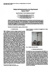
The function of an intermediate switching node is to deliver network packets from the node's inputs to the node's outputs in accordance with the destination addresses and credits availability or to keep incoming packets in the internal bu�ers until their delivery becomes possible. Each node consists of address decoders, arbiters, credit pools, and the data path (Fig. 1). All data and control bits in the CNET (W�85 bits altogether) are transmitted along separate wires (Fig. 2A). Every packet has: an indication bit which is used to distinguish a valid packet with all \0" bits from an empty frame; a number of control bits, including a continuation bit allowing several packets to form a chain in a \worm-style" fashion; 15 address bits; the payload (not interpreted by the network), and a parity bit. A parity check may be AA CA
decoder
arbiter
pool
CA
AB CB
decoder
arbiter
pool
CB
DA0 DB0 DA1 DB1
2x2 2x2
DAn DBn
2x2 credit buffers
Fig. 1. Internal switching node structure. AfABg | network address; CfABg | credit messages; DfABgf0: : :ng | payload.
Dj I C0 ... A0 ... An D0 ...
Dn
Ack1 R’
I
Di P
ctrl. address
C1
P1
C2
P2
D
A0 data
C
parity
data
DC R
C
indication
Ack2
Cr Merger
Dn ... Dn ... Dn ...
...
...
...
...
...
...
...
...
...
...
...
...
...
...
...
Dj I C0 ... A0 ... An D0 I C0 ... Di Dj P ... ... A0 ... An D0 ... Di Dj I C0 ... P ... A0 ... An D0 ... Di P
Rd2
Rd1
...
time
(A)
(B)
Fig. 2. CNET packet format: A) bit assignment and B) actual front shape.
necessary when crossing chip boundaries. The actual shape of a data front is inclined with respect to time (Fig. 2B): the central bits (indication, control, and address) are the rst to arrive. This facilitates the readout and increases the throughput. We propose a node architecture with input data bu�ering. An incoming packet is accepted by the node and placed into the rst unused position in an elastic FIFO queue. Input queues Qa and Qb (Fig. 3) are maintained on a per-link basis. The two FIFO queues for each bit share a 2�2 switch (Sw) which also serves as the head bu�er for each queue. The switch is based on two D2 ip- ops. A packet from any queue can be sent to any of the two outputs. Packets from both bu�ers can be dequeued if they do not go to the same output. All preceding packets in the queue are shifted towards the head of the queue. A 1-bit data path with Nc credits can be implemented in RSFQ using 14Nc +40 Josephson junctions. III. Address Decoding
Address decoding and routing in banyan networks are very simple. The switching node must examine only one bit of the packet's destination address. This bit is used exactly once and does not have to be propagated to the next switching node. Instead, since all switching nodes can always use bit A0 for routing, the entire address may be shifted towards the indication bit, and the binary address of the input queue (\0" for A or \1" for B) can be
Fig. 4. Banyan node address decoder.
inserted into the packet's header to trace its source. The situation is di�erent for the mesh networks, where some or all bits of both incoming packets have to be examined. Our implementation of the address decoder (Fig. 4) is based on a D ip- op with complementary outputs (DC). The ip- op stores the rst address bit A0 and is triggered by the indication I which should arrive after some delay. The resulting routing request R or its complement R' generated by the ip- op will not immediately go to the arbiter. Instead, it must rst be synchronized with the acknowledgment Acki to be sure that the arbiter is ready to accept the new request. The synchronization is performed by the coincidence elements C1 and C2 (also known as Muller \C" elements). The synchronized requests Pi also serve as clock signals Rdi for the data path. The acknowledgment bits are merged to produce credit message Cr for preceding network nodes. 30 Josephson junctions are necessary for an RSFQ implementation of one address decoder. IV. Contention Resolution
A contention occurs when packets from both input queues need to be sent to the same output. Contentions in our banyan node are resolved by arbiters (Fig. 5A). The problem of fair arbitration is well known in the theory of asynchronous (not-clocked) systems: the time required to choose one of two concurrent signals is recipL1
D1
Rq1
P1 L
D
U
C J3 Ack1
J5 L1
Ack2 L
D
U
J4
J1
Q
J2
P2
Rq2
D2
L2
A)
B) U/Q
I1 L2
LD
U
L U
FIFO queues Qa
I1
D
Sw
J1
J2
D
J3 L
A
D
D
D
D2
A’
D
D
D
D
Q
L D/Q
Qb B
L1 J4
D2
B’
Fig. 3. CNET data path (one bit, 4-credit con guration).
C)
U
D)
Fig. 5. Arbiter: A) schematics of the arbiter, B) schematics of a concurrent D ip- op, C) schematics of the lock cell, and D) Moore diagram of the lock cell.
rocal to the time distance between these two signals. It is important to separate the requests in time and synchronize them with some clock. The separation and synchronization is managed by a pair of specially designed D
ip- ops D1 and D2. A clock signal runs permanently in the loop between the two ip- ops and polls them. If the polling signal and a data bit come almost simultaneously (i.e., close enough in time), the Josephson comparator J2/J4 (Fig. 5B) is unable to decide whether the ip- op has data or not. In this case, both Josephson junctions in the comparator are switched. This situation satis es us: if a request is being stored in the ip- op, we can either read it out immediately or wait for the next clock cycle, but we need to compensate the erroneous behavior of the comparator using a \back-up" Josephson junction J5 which otherwise does not participate in the operation. The synchronizing pair of the D ip- ops guarantees that the time interval between two requests Rq1 and Rq2 is at least Tl /2, where Tl is the period of the clock oscillating in the loop. Now we can consistently use a \traditional" locking mechanism. If request Rq1 is the rst to pass the synchronizer, and if locking cell L1 is not locked, the request passes through the cell, generates a request for credit P1 , and locks cell L2 . Tl must be long enough to ensure that the other request does not enter cell L2 before it has been locked. If the cell is locked, then the request is stored in L1/J4 (Fig. 5C,D). Acknowledgment messages from the credit pool concurrently unlock the arbiter. If a pending request has been stored in the locked cell, it is released, locks the opposite cell and generates its own request for credit. The design of an arbiter requires 24 Josephson junctions. V. Credit Management
Credit management in the banyan switching node is handled by credit pools (Fig. 6A). The credit pool is symmetric with respect to two request inputs Rq1 and Rq2. The internal state of the pool, namely, the number of interferometers with no SFQ quanta (Fig. 6B), re ects the credits availability. Initially, there are Nc credits in the pool (all interferometers are empty). If there are spare interferometers in the pool, every request Rqi decrements the number of credits (an SFQ is stored in the rst available interferometer), generates an acknowledgment Acki (used by the arbiters), and propagates to the output Pi as a permission to send the packet to the corresponding link. Otherwise, the request is bu�ered at the request input waiting for a credit message on input Cr. Every credit message increments the number of credits up to Nc. A nice feature of such a chain structure is that it operates in a stack-based manner: if a request can be granted, it is granted locally (i.e., as fast as possible). If the requests rate is close in average to the credits rate, the throughput of the credit pool is determined only by the
Rq2
P2 J1
W2
Cr/P2
Ack2 Rq2 Cr
0
Rq2/P2
Cr/P1
Cr Rq1
Rq2/P2 Ack1 2 P1
Rq1
(A)
W1
1 Cr
Rq1/P1 Rq1/P1 (B)
Fig. 6. Credit pools: A) schematics of a credit pool with 3 credits and B) Moore diagram of a credit pool with 2 credits.
switching time of Josephson junction J1, not by the number of elements in the chain. On the other hand, if requests arrive more frequently than credits, then the credit pool mainly stays in states \W1" and \W2", and it takes time proportional to Nc for a credit message to propagate from the input Cr to the head of the chain. Our implementation of the credit pool requires Nc +7 Josephson junctions. VI. Performance and Real Estate Evaluation
Table I summarizes the number of Josephson junctions necessary to implement a 85-bit-wide, 40-credit banyan node, and power dissipated by the node (assuming 0.8 mV d.c. bias voltage). 98% of real estate and 99% of power is claimed by the data path. Therefore, we can expect that an RSFQ implementation of a mesh node with a similar data path will have similar characteristics. The estimated size of an internal node implemented using a hypothetical 0.8 �m technology is 3.0 mm�1.74 mm. The estimation is based on the actual prototype node designed using a 3.5 �m technology (see Section VII.) The throughput of the node is determined by the length of two critical paths (Fig. 7): one is shared by two adjacent nodes (path \A", from the address decoder to the arbiter, to the credit pool of this node, to the credit pool of the previous node, to the switch of the previous node, and back to the address decoder), and the other is completely contained in one node (path \B"). The length of either path linearly depends on the number of credits. Our simulations show that for a 40-credit con guration, the length of the longer path is 240 ps, and the length of the shorter path is 29 ps. However, the longer path may have up to 40 credit messages in it, so its length must be divided by 10. Therefore, the average throughput of a banyan node as currently designed is one packet in every TABLE I HARDWARE AND POWER BUDGET FOR A 40 CREDIT NODE Part Quantity Per Part Total name #JJ P, �W #JJ P, �W Data bit 85 600 54 27,000 4590 Decoder 2 30 2 60 4 Arbiter 2 24 2 48 4 Credit pool 2 47 10 94 20 Grand Total: 27,202 4,620
A Credit pool
Address decoder
3.06
Credit pool
Arbiter
3.07
3.08
3.09
3.10
1.0
1.0
0.8
0.8
0.6
0.6
0.4
0.4
0.2
0.2
Address decoder
B Buffer
Switch
Buffer 1−B.E.R.
Switch
Fig. 7. Critical paths in a 2-credit banyan node.
29 ps. The time spent by a packet inside the switching node (service latency) on average equals to 109 ps. Our recent research indicate that the performance of the node may be improved by using more aggressive schematics and layout design. The average throughput may be increased to one packet in every 15 ps. VII. Experimental Results
We began the experimental implementation of one banyan node with the data path. The following fragments have been fabricated using 3.5 �m niobium trilayer technology [6], and tested at low frequency: 2 � 2 switch circuit (175 Josephson junctions, Fig. 8); 1-bit-wide 2-credit data path (425 Josephson junctions); and 2-bit-wide 2credit data path (530 Josephson junctions). Both data path fragments include internal and external microstrip lines, drivers, and receivers. Each circuit fragment has two independent d.c. bias lines: one feeding the circuit itself (\the kernel"), and the other feeding auxiliary devices (SFQ/dc and dc/SFQ converters; \the frame"). The parameter margins for the 2�2 switch are �15% for the frame, and �23% for the kernel. Simulated margins for the kernel voltage are �30%. Experimentally measured kernel voltage margins for the 1-bit-wide data path are �21% (Fig. 9). The 2-bit frag-
0.0 2.00
0.0 2.01
2.02
2.03
2.04 UKern, mV
Fig. 9. Experimentally measured low-frequency bit error rate in 1-bit-wide data path as a function of d.c. bias voltage Ukern .
ment was also partially operational (four channels out of eight; kernel voltage margins are �2.5%, frame voltage margins are �13.7%), and the functionality of that fragment was mostly limited by failing dc/SFQ converters. VIII. Conclusion
We have proposed and studied in detail an RSFQ implementation of an internal CNET switching node. The node has reasonable timing parameters which can be further improved, and negligible area and power dissipation which makes it suitable for use in a hypothetical peta ops computer. The architecture of the node can be used with little or no changes in both blocking and non-blocking banyan and mesh networks. Acknowledgment
This work was performed for the Jet Propulsion Laboratory, California Institute of Technology. The authors gratefully acknowledge the valuable help and cooperation of P. Bunyk, Prof. K. Likharev, and Dr. L. Wittie. References
Fig. 8. Microphotograph of the fabricated 2�2 switch.
[1] K. Likharev and V. Semenov, \RSFQ logic/memory family: a new Josephson junction technology for sub-teraherz clock frequency digital systems," Applied Superconductivity, vol. 1, pp. 3{28, Mar. 1991. [2] G. Gao, K. K. Likharev, P. C. Messina, and T. L. Sterling, \Hybrid technology multithreaded architecture," in Proc. Frontiers`96, (Annapolis, MD), pp. 98{105, 1996. [3] M. Dorojevets, P. Bunyk, D. Zinoviev, and K. Likharev, \Peta ops RSFQ system design." Report ETE-04 to ASC'98, unpublished, Sept. 1998. [4] L. Wittie, G. Sazaklis, D. Zinoviev, and K. Likharev, \CNET: Designing an RSFQ switching network for peta ops computing." Report EOD-03 to ASC'98, unpublished, Sept. 1998. [5] D. Zinoviev and M. Maezawa, \Application of credit-based ow control to RSFQ micropipelines." Report EDE-04 to ASC'98, unpublished, Sept. 1998. [6] \HYPRES design rules." Available from HYPRES, Inc., 175 Clearbrook Rd., Elmsford, NY, 10523.