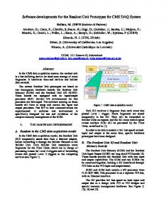
Design and Performance Testing of the Read-Out Boards for the CMS - DT Chambers. C. Fernández, J. Alberdi, J. Marín, J. C. Oller, C. Willmott Lab. Electrónica y Automática. CIEMAT. Avda. Complutense, 22. 28040 Madrid. Spain.
[email protected]
Abstract Read-out boards (ROB) are one of the key elements of readout system for CMS barrel muon drift chambers. To insure proper and reliable operation under all detector environmental conditions an exhaustive set of tests have been developed and performed on the 30 pre-series ROB´s before production starts. These tests include operation under CMS radiation conditions to detect and estimate SEU rates, validation with real chamber signals and trigger rates, studies of time resolution and linearity, crosstalk analysis, track pattern generation for calibration and on-line tests, and temperature cycling to uncover marginal conditions. We present the status of the readout boards (ROB) and tests results.
I. INTRODUCTION Muon tracks along the CMS DT-chambers generate electric pulses that go through a large and complex path of signal conditioning, time measurement digitalization, encoding and multiplexing to reach the final steps of data acquisition [1]. Muon barrel Front-End electronic provides discriminated signals to perform a precise time measurement in the ReadOut Boards (ROB). These signals are also converted and sent to the trigger logic that is placed nearby the ROB in readout crates attached to DT-chambers inside the iron yoke. Each ROB can digitize up to 128 differential signals and drives this timing and positional information to a multiplexer (Read-Out Server, ROS) in the detector periphery. This is the first step of processing towards muon track reconstruction at the DAQ level [2].
II. SYSTEM DESCRIPTION A. Time to digital conversion. Read-Out Boards are built around a 32-channel high precision TDC [3], developed by the CERN/EP Microelectronics group. This highly programmable HPTDC is based on the Delay Locked Loop (DLL) principle and provides a relative time measurement at L1A arrival of each hit inside a
programmable time window, chosen to accommodate the maximum drift time. One of the main features of this TDC is the ability to handle overlapping triggers, as an individual hit may fall inside several time windows. A fast and efficient search mechanism has been implemented to develop this task. In the low resolution mode that we are using, the TDC has a time bin of 0.78 ns at 40 MHz, which gives a 265 ps resolution. Other remarkable features are independent four 8channel storing groups, large output buffer, JTAG programming, flexible signal interface and readout modes, clock PLL, etc.
B. ROB description. ROB configuration comprises 4 HPTDC´s in a clock synchronous token ring, where one of them is programmed as master, controlling the token of the read-out data_ready/get_data handshake protocol. There is also a failsafe bypassing mechanism in case one TDC fails that guarantees the operation of the rest of the TDC´s on the board. LVDS receivers DS90LV048
... Trigg Evrst Bcrst Reset JTAG ....
TDC 1
...
Data ready get data
...
FPGA
TDC 2
TDC 3
20MHz
CLK LVDS 40MHz
TDC 4
...
Serializer
LVDSlink DS92LV1021
Figure 1: Read-Out Board diagram.
The JTAG interface for TDC programming and monitoring is included in a parallel bus shared by every ROB in a DT-chamber. This bus also carries among others: trigger signal, event reset, bunch reset and other test pulse control signalling. An Altera MAX FPGA controls the readout handshake protocol and also manages the track pattern test, enabling the
appropriate channels to generate simulated tracks at the LVDS signal receivers on the board (DS90LV048). A byte-wise read-out scheme is used for the TDC to drive their data directly into a 20 MHz serializer (DS92LV1021).
170 160 150 140
ns
ROB is also equipped with an overcurrent protection circuitry that disables 2.5V and 3.3V power supply to prevent from high currents due to short-circuits, latch-up´s or any other circumstance. After a time, power supply is reinitiated. Temperature, voltage and 2.5V current can be continuously monitored through a sensor on the board (DS2438).
100 ps time sweep
130 120 110 100
110
120
130
III. ROB FUNCTIONALITY TESTING With the aim of checking ROB design and to define and develop production acceptance tests, a set of test jigs have been built. 30 pre-series ROB have been tested thoroughly to establish a definitive design for the production of the final 1500 ROB´s. Appropriate hardware and software has been implemented to perform exhaustive ROB testing for monitoring, controlling and data acquisition. Some purpose-dedicated boards have been built to accomplish system configuration, signal pattern generation and TDC data readout from VME (Figure 2).
140
150
160
ns
Residuals 100
σ = 0.26 ns 75
50
25
0
This basic structure is flexible enough to develop a large number of different tests that have proved extensively ROB functionality and also behaviour under diverse environmental conditions. PULSES
CLK
128 CHANNELS
ROB-128
40
CONTROL
0
0.1
0.2
0.3
0.4
0.5
0.6
0.7
0.8
0.9
ns
Figure 3: Linearity and time resolution measured for the HPTDC.
B. Track pattern tests
2
1
ROBUS
-0.8 -0.7 -0.6 -0.5 -0.4 -0.3 -0.2 -0.1
ROS
PATGEN
PCI-VME PC
Figure 2: Scheme of the test jig implemented for ROB testing.
A. Time resolution and linearity The effective time resolution of the TDC has been measured using a pattern generator (Tektronix DG2020, clock jitter < 50ps). An example of this test is presented in figure 3, which shows linearity and resolution measurements over a small dynamic range when a hit is delayed in steps of 100 ps. From the histogram of the residuals we obtain the TDC RMS resolution, which turned out to be 260 ps, in agreement with TDC specifications (265 ps) [3].
In order to simulate test pulse generation that will be performed for testing and calibration of the chambers, a track test mechanism has been implemented in the ROB. The track pattern sequence is generated enabling particular groups of 4channels receivers in each event. We checked the proper operation of this test that in addition has been very useful during FPGA irradiation as it makes use of basically the whole logic of the FPGA.
C. Crosstalk measurements We were concerned about possible timing influence on any channel due to their neighbours. The presence of a signal close in time to another in neighbour channels may modify the time measurement due to interference at any level: cables, PCB, receivers or TDC. We have tried to measure this possible effect sending two signals on consecutive channels separated by a distance in time “x” as it is shown in figure 4. We have taken measurements at different time separations and comparing them with the time of the reference signal.
In the second test period a total amount of 4.5· 107 events were taken. Due to the beam structure the number of overlapping triggers was much higher, and we proved that the TDC can handle them properly. We also had two noisy channels in the chamber (~MHz) that eventually occasioned TDC buffer overflows. We checked that HPTDC can flag this overflow and that such noise affects only one 8-channel group, without any loses of hits in other groups.
x
Figure 4: Representation of the time separation between neighbour channels.
The results obtained (figure 5) show different overlapped effects. Some of them are due to set-up external to the ROB, but we can see one spike near 0 ns separation that is originated in the ROB. This spike is 15 ns half width, that is, the influence region of the two signals, and about 150 ps height. As a consequence we find that the maximum influence due to a neighbour signal is in any case less than 200 ps, which is well below the TDC resolution.
In figure 6 it can be seen the typical drift-time distribution of a cell obtained from the test beam data.
Signal Shift (ns)
0,20 0,15 0,10 0,05 0,00 -0,05 -0,10 -200
-150
-100
-50
0
50
Time from Noise to Signal (ns)
Figure 5: Crosstalk results: signal time measurement shift vs. time separation between channels.
D. Test beam validation Two different test beams have validated HPTDC operation and ROB design. The readout system was placed with one ROB connected to 96 channels of three superlayers of an MB2 chamber operated under normal gas and voltage conditions at CERN Gamma Irradiation Facility (GIF). Tests were made under two different beam conditions. In the first place at P2B (Oct. 4 to Oct. 23, 2001) with a non structured beam of about 6000 triggers/spill, that is, 1200 triggers/s, with spill duration of 5.1s in periods of 16.8 s. In the second place during P2C period (Oct. 25 to Nov. 4, 2001) where the beam had a 25 ns structure, with about 26000 triggers/spill, i.e. 5000 triggers/s. During the first test beam period 3.5· 106 events were registered and confirmed the correct operation of the system, with no TDC errors, no FIFO overflows and only a few overlapping triggers. Considering that the matching window was set to 800 ns and we had about 1 trigger/ms, the probability of having overlapping triggers was only 8 10-4. Data were taken also with gamma irradiation over the whole chamber, to simulate background under normal LHC operating conditions and the effective noise increase was observed but had no effect on TDC behaviour.
Figure 6: Drift-time distribution of a cell.
We conclude that the present ROB design with four HPTDC´s works satisfactorily. It can stand high hit rates, even with noisy channels. Besides, this noise affects only one group (8 channels) and buffer full is flagged, so the system can be notified.
IV. ENVIRONMENTAL CONDITIONS TESTING A. Radiation tests Besides standing high hit and trigger rates the ROB will have to operate in the muon barrel under particular environment conditions. Although the magnetic field is very intense in this region, it does not have a major influence on this electronics. Instead, particle radiation has a critical effect over electronics and thus its tolerance has to be tested, mainly as most of the ROB devices are commercial chips and not even HPTDC is implemented in a technology guaranteed to be radiation hard. The total ionizing dose (TID) expected in 10 years of operation at full luminosity is below 1 Gy and the neutron fluence over 10 years about 1010 cm-2. Irradiating with 60 MeV protons is considered an effective method of testing the electronics for total dose effects, displacement damage and single event upsets (SEU) [4]. These tests have taken place at the CRC of the Université Catholique de Louvain (UCL).
Accordingly, results are very satisfactory as imply an error rate of less than 1 per day in the whole detector.
The temperature tests have been performed in an environmental chamber where the ROB could be fully operated and monitored. Two kinds of tests have taken place: firstly, a soft temperature cycling (0.2ºC/min) between 0º and 70ºC which are the temperature margins of some of the devices, in order to observe their behaviour without damaging them. Furthermore, we are making life time tests at 105ºC to find out failure mechanisms in an accelerated stress test. The aim of this test is to discover the most probable failure modes to know the acceleration factor that we have to use to eventually perform an accelerated stress screening [5]. At the moment one ROB has stood at 105ºC about 600 hours without failing. Cycling tests have allowed us to study the time measurement variation with temperature. In figure 7 we can see how the higher the temperature, the smaller the time measurement, that is, the sooner the hit signal has been digitalized. The maximum time shift is of 1 ns between 0ºC and 70ºC, but the slope is different depending on the temperature. There is an area of faster variation around 40ºC, although this temperature is slightly different depending on each TDC. In this region of higher slope we find a variation up to 45 ps/ºC, while the average variation is around 15 ps/ºC.
481,4
50 40 30 20
481,2 481
0 -0.05 0
20
40
60
80
-0.2 T e mperature (ºC)
Figure 8: Time shift relative to 20ºC time measurement due to LVDS receivers.
It is shown in figure 9 how the output from the Micrel low voltage regulators is very stable with temperature. The maximum voltage shift obtained is below 0.2 mV/ºC. 2 .5 volts
2,486 2,485 2,484 2,483 2,482 2,481 2,48 2,479 31,5
32,5
39
39 50 T e m p e rature (ºC)
50,5
65
50,5
65
3.3 volts
3,282 3,281 3,28 3,279 3,278 3,277 3,276 3,275 3,274 31,5
32,5
39
39
50
Temperature (ºC)
70
Temperature
Time measurement
481,6
0 .1 0 .0 5
Figure 9: Output regulator voltage vs. temperature.
80
60 481,8
0 .1 5
-0.15
Each ROB consumes around 4 watts that will be dissipated in the crates through a water pipeline cooling. Although this refrigeration system will guarantee a stable temperature inside the crate, some temperature tests have been made to characterize ROB behaviour under non-normal environmental conditions.
482
T ime shift relative to 20º
-0.1
B. Temperature cycling
482,2
temperature, having a contribution to total variation of around 30%.
time (ns)
Every component from the ROB have been tested with a total fluence of 5 1010 protons cm-2. During irradiation ROB operation was continuously monitored and only one SEU was observed during the irradiation of one TDC, and the device was recovered after reprogramming.
10 0
Figure 7: Temperature cycling and time measurement of one TDC channel.
Analysing this temperature variation we have seen that this shift is partly due to the LVDS receivers (DS90LV048). Figure 8 shows how its propagation delay depends on chip
V. CONCLUSIONS The set of tests developed have allowed an exhaustive verification of the Read-Out Boards, including not only the overall design but also other important aspects, as adequate PCB routing, device operation and tolerance to radiation and environmental conditions. The whole ROB functionality has been tested with very satisfactory results, demonstrating proper operation beyond the conditions expected in CMS DT-chambers. As a result of these studies the final ROB design is ready for production. In addition a subset of these tests will be used at the factory as the acceptance tests for every produced board.
I. REFERENCES [1] . CMS. The Muon Project. Technical Design Report, CERN/LHCC 97-32. December 1997. [2] CMS. The Trigger and Data Acquisition project. Volume I. The Level-1 Trigger. CERN/LHCC 2000-038. December 2000. [3] Manual Version. High Performance Time to Digital Converter. Version 2.1. J. Christiansen. CERN/EP – MIC. July 2002. [4] CMS COTS Tutorial and Workshop, 16-17 Nov 1999: http://cmsdoc.cer.ch/~huu/tut1.pdf http://cmsdoc.cer.ch/~huu/tut2.pdf http://cmsdoc.cer.ch/~huu/tut3.pdf http://cmsdoc.cer.ch/~faccio/tutorial.pdf http://cmsdoc.cer.ch/~faccio/proced.pdf http://cmsdoc.cer.ch/~gst/cmscots/Jkinnison_slides.p df [5] Electronic Component Reliability. Jensen, F. John Wiley & Sons, 1995.