Design and simulation of mems shunt capacitive switch for lower switching time DOI: http://dx.doi.org/10.17993/3ctecno.2019.specialissue.15
DESIGN AND SIMULATION OF MEMS SHUNT CAPACITIVE SWITCH FOR LOWER SWITCHING TIME
Kurmendra Department of Electronics & Communication Engineering, Rajiv Gandhi University, Itanagar, (India) E-mail:
[email protected] Rajesh Kumar Department of Electronics & Communication Engineering, North Eastern Regional Institute of Science & Technology, Itanagar, (India) E-mail:
[email protected]
167
Design and simulation of mems shunt capacitive switch for lower switching time DOI: http://dx.doi.org/10.17993/3ctecno.2019.specialissue.15
ABSTRACT As Demand of High speed devices increasing for RF and satellite communications with better accuracy, MEMS technology is considerd to be emerging technology to fulfill that need. In this paper, A MEMS shunt capacitive switch with fixed- fixed beam have been designed and simulated for numerous parameters. The parameters for study are Selection of beam material for the switch, air gap distance between electrodes and importantly the actuation voltage. For studying the effect of air gap and beam width on switching time , the air gap was varied from 0.6 µm to 2.0 µm and beam width from 1 µm to 50 µm. For an actuatiuon voltage of 10.5 V and air gap distance of 0.6 µm, switching time result is 0.2 ns for spring constant equal to gold material.Study also considers the effect of increasing beam dimension in terms of width for a constant gap height. This syudy will be helpful for designing a MEMS capactitive switch for higher speed and for selection of proper dimension to get better performance. KEYWORDS Beam, Electrode, MEMS, RF, Switch, Switching time. 1. BACKGROUND RF MEMS switches are considered to be a potential switching device for high speed switching applications. These types of switches have capability of replacing traditional MOSFET switch, Tunnel Switch and Pin-diode based Switch [1-4]. Many actuation mechanisms such as optical actuation, electrostatic actuation, thermal actuation and actuation by force are used for MEMS switch devices [5]. Mostly used actuation mechanism is Electrostatic actuation since it has many practical advantages such as low power requirement and small sized device. Despite of having various advantages, MEMS switches lack in switching speed and requirement of low pull in voltages [6-7]. Various techniques are currently being used to overcome the problems associated with these switches. Low spring constant materials are considered to be prominent source of material for low pull in voltage but at the same time, the switch suffers with low speed and reliability of device [8-9]. The switching speed can be increased by using a switch beam with lower mass. The switches made up of low mass materials relatively posses high speed compare to higher spring constant materials [10]. A. Kundu et al. (2010) have designed a new switch where the top metal and central conductor both are movable and considerable improvement was found in actuation voltage requirement and switching time as 20 % down [11]. S. Sekhar et al. (2011) designed electrostatically actuated MEMS switch and experimental as well as FEM analysis were done. Their observation concludes that pull up time is more than pull in time which is somewhat counter part because in case of pull in there is much larger electrostatic force compare to pull up restoring force at release time [12]. C. Siegel et al, have provided the switching analysis of MEMS cantilever-based switch and article reports that measured switching time in the air medium for the switch is below 75 µs which is also dependent of actuation voltage. Semiconductor effect in actuation path is responsible for 60 µs and switching time also depends on bending of the membrane [13]. Markus et al
168
Design and simulation of mems shunt capacitive switch for lower switching time DOI: http://dx.doi.org/10.17993/3ctecno.2019.specialissue.15
(2014) have reported that they have designed a MEMS switch which requires very low pull in voltage as 5V and switching time is less than 10 µs at 5 Ghz. The designed switch is very much usable for RF applications [14]. K. Guha et al. (2015), have proposed meander-based switch made up of Aluminum membrane and the study was done for providing very less switching time as 3 µs for actuation voltage of 5V [15]. K. Guha et al. (2018) have also proposed a new analytical model for analysis of switching time for perforated MEMS switch. They have presented modified Mejis and Fokkema’s model and the model is capable of evaluating switching time for uniform as well as nonuniform meander-based switch designs. Results were plotted between switching time and displacement for uniform and non-uniform meander designs with different Vs and materials [16]. In this article, a Shunt capacitive MEMS switch is designed which is capable of working at very high frequency range 20- 100 Ghz approximately.. The MEMS switches have also been designed by other researchers having different kind of structures. But these designed switches have many disadvantages such as insertion loss, isolation loss, return loss and very important switching time.The previously published articles in the domain have addressed about losses associated with their designed switches but only a few articles have presented switching time analysis [refer table.2 ]. Firstly, the structure presented in this paper was optimized in terms of different size dimensions as well as the selection of materials involved a rigorous literature review and were so chosen that the disadvantages associated with previously designed switches could be overcome [17-18]. After designing the switch, we have done many static analysis such as pull in voltage analysis and RF analysis which have already been published in a journal of repute [21]. We found that the designed switch is showing a great improvement in terms of insertion, isolation and return loss parameters [21] Here, An analysis of the MEMS switch considering switching time is presented in terms of dielectric constant, voltages, air gap and width of the beam material. In the proposed work we have taken most promising issue related to the MEMS switch that is switching time. Our work has shown tremendous improvement in terms of switching time as well as losses associated with. The switch designed on MEMS technology generally have one disadvantages of having larger switching time which has been significantly improved and which is presented in the paper.
2. DESIGN OF PROPOSED MEMS SHUNT SWITCH AND WORKING
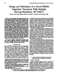
Figure 1. Schematic of proposed RF MEMS shunt switch.
169
Design and simulation of mems shunt capacitive switch for lower switching time DOI: http://dx.doi.org/10.17993/3ctecno.2019.specialissue.15
The schematic of designed MEMS shunt switch is shown in the Figure1. The switch consists of silicon substrate, dielectric layer (Si3N4) placed over CPW transmission line and gold material is used for beam bridge, beam supporting anchors and transmission line central conductor as well as CPW ground. There is an air gap g0 between Au top electrode and dielectric layer above CPW signal line. The switch is actuated by using very common actuation technique that is electrostatic actuation. Initially there will not be applied any actuation voltage and the signals in the signal line go without any interruption. When a voltage is supplied between beam and down electrode (CPW signal line) as shown in fig.1, an electrostatic force is developed on switch membrane (beam) and this force pulls down the beam. When this beam touches dielectric material, it forms a path between signal line and beam to the CPW ground for signals coming from CPW signal line, thus signal goes to CPW ground, the switch is called to be in OFF state. In the actuation and switching analysis, the supply voltage, air gap and material properties play very important role.
3. FORMULATION & SWITCHING PERFORMANCE ANALYSIS RF MEMS switch generally offers a better performance characteristic when considered for low insertion loss, high isolation and low return loss. The performance characteristics of the switch does not only depend on these losses but also depends on the speed to make open and close circuit, generally termed as switching speed. Switching speed can be improved by employing different techniques such as TMPS technique [11] where the electrode as well as signal conductor move to offer a better switching speed. In this section, we are going to include some important switching equations for switching time analysis. The switching time in terms of applied voltage (𝑉𝑠), pull in voltage (𝑉𝑝) and operating frequency can be given as [19] 𝑉𝑝 𝑡𝑠 = 3.67 𝑉𝑠𝜔0 (1) Where, ′𝑡𝑠′ is the switching time of the designed switch, 𝑉𝑝 is the pull in voltage (10.5 V), Vs is the supplied voltage (𝑉𝑠 = 1.4𝑉𝑝) and 𝜔0is the operating frequency or resonance frequency of the switch. Spring constant of the material specifically used for switch membrane is important parameter for the switching time analysis of the switch. An equation for switching time in terms of spring constant of beam membrane can be obtained by putting 𝑉𝑠 = 1.4𝑉𝑝 𝑘
1/2
and 𝜔0 = (𝑚𝑒)
[16]
𝑚𝑒 1/2
(2) ) Where, ‘𝑚𝑒’ is the effective mass and ‘𝑘’ is the spring constant of the beam membrane for the designed switch. The switching time in terms of gap height g0 and width of the membrane can be approximated and give as [11] 𝑡𝑠 = 2.62 (
1
𝑘
4𝑚𝑒∗𝑔03
𝑡𝑠 = 𝑉𝑠 (
Ɛ0∗𝑊
1/2
(3)
)
170
Design and simulation of mems shunt capacitive switch for lower switching time DOI: http://dx.doi.org/10.17993/3ctecno.2019.specialissue.15
Where, 𝑔0 is the initial airgap between the membrane and signal line, Ɛ0 is the free space permittivity and 𝑊 is the width of the switch beam membrane. The equations which are provided above helps in analyzing the switch performance in terms supplied voltage, spring constant, air gap heights and width of the top metal beam.
4. RESULT & DISCUSSIONS A MEMS capacitive shunt switch was designed as shown in the Figure 1. The design parameters and materials used in the proposed switch is given in the Table.1. The operating frequency of the switch was calculated using coplanar waveguide calculator [20] and was verified using COMSOL Multiphysics 5.1 software. Table 1. Design parameters and materials used of the proposed switch. Serial number Design Parameter Materials used Value (in µm) 1 Beam length 100 Gold 2 Beam width 5 Gold Beam thickness 1 Gold 3 Coplanar wave guide 50-10-1 Gold 4 Dielectric thickness 0.4 Si3N4 5 Substrate thickness 5 Silicon 6 Air gap 0.6 ------7 Supply voltage for 14.7 V ------8
switching analysis (𝑉𝑠
=
1.4𝑉𝑝)
62 Ghz approx.
--------
Operating frequency
Figure 2. Switching time variation in terms of applied voltage (Vs = 1.4 Vp).
In the Figure 2, result for switching time for the sweep of 0-15 V in supply voltage is given. From the plot we can understand that in the voltage range 05 V, switching time is more compare to switching time for 5-15 V. our designed
171
Design and simulation of mems shunt capacitive switch for lower switching time DOI: http://dx.doi.org/10.17993/3ctecno.2019.specialissue.15
switch posses pull in voltage about 10.5 V for which we obtain the switching time as low as 0.2 ns.
Figure 3. Switching time variation for varying spring constant of beam material.
Figure 3 illustrates, the curve between spring constant for the beam material and switching time. It can be clearly concluded that the switch made up of high spring constant value is going to require very less switching time compare to beam materials with low spring constant thus enables switch to work at high speed.
Figure 4. Switching time as function of varying air gap height between beam electrode and dielectric layer above signal line.
172
Design and simulation of mems shunt capacitive switch for lower switching time DOI: http://dx.doi.org/10.17993/3ctecno.2019.specialissue.15
Figure 4 depicts the result between the air gap heights and switching time for designed switch, as per the literature the lower the gap between top and bottom electrode demands lower switching time but lowering of this gap is permissible only up to certain limit since there should be enough gap to apply supply voltage (𝑉𝑠 = 1.4𝑉𝑝). In Figure 4 it can be observed that as we are approaching towards higher air gap, the requirement of switching time is also increasing which considerably reduces the speed of the switch.
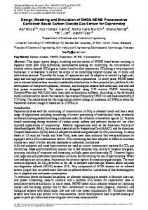
Figure 5. Switching time variation for different beam width for air gap go,g1,g2 and g3 .
As per the equation (3) of the section.3, we can see that the beam width does play an important role for switching speed or switching time of the device. In the Figure 5, the result for varying width of the beam and switching time is plotted for constant air gap (g0 = 0.6 um, g1 = 1.0 um, g2 = 1.5 um & g3 = 2 um). Arrow sign in the Figure 5 is kept for showing increasing air gap height direction. as we keep on increasing the width of fixed- fixed beam of the switch, the switching time required is getting lesser. While choosing greater beam width, we should note that for a miniaturized device, there is need of using beam with lesser beam width. The effect of increasing air gap between beam electrode and lower electrode are considerably high for the same sweep of beam width. In the Figure 5, it can be observed that as we are increasing this gap the switching time requirement is going to be very high compare to lesser beam width. Thus, there is a need for trade off between the switch parameters such as air gap, beam width, applied voltage and selection of materials for improving the switching time which ultimately improves the switching speed.
173
Design and simulation of mems shunt capacitive switch for lower switching time DOI: http://dx.doi.org/10.17993/3ctecno.2019.specialissue.15
Table 2. Compared results obtained with various losses, Frequency of operation and switching time.
Sr. No.
Insertion loss
Isolation
Return loss
Switching time
1
0.29 dB
20.5 dB
-------
Not done
Frequency of operation 35 Ghz
2
-0.4 dB
80 dB
-------
Not done
20 Ghz
3
-0.44 dB
- 20 dB
- 16 dB
Not done
0.6 – 40 Ghz
4
-------
--------
---------
< 10 us
5 Ghz
5
-0.05 dB
-12 dB
-45 dB
0.2 ns
61.5 Ghz
References
Muhua li et al [2017] [22] Guha et al. [2016] [23] T. Laxmi Narayana et al [2017] [24] M. Gatzsch et al [2014] [14] Our work
A comparision have been shown in Table 2 between our designed MEMS shunt capacitive switch and switch reported in other articles. Through comparision it was found that our designed switch results in a much improved performance in terms of losses and switching speed.
5. CONCLUSION The paper presents the performance analysis of a new and simple shunt capacitive switch design in terms of switching time. The analytical equations were presented for the analysis. Specifically switching time was analytically analyzed on four parameters such as supplied voltage, spring constant of material, initial air gap heights and width of the material. From the analysis of the results, it can be concluded that trade off between supply voltage and switching time is required since high switching is achieved for high supplied voltage but a device with high supply voltage is not recommended. High spring constant materials results in less switching time which practically improves switching speed. A switch with larger beam width and lesser air gap is efficient for high switching speed. This study will surely be useful for researchers working in the area of MEMS switch design for high frequency applications. 6. ACKNOWLEDGEMENT This research work has been carried out in MEMS laboratory, Department of ECE, Rajiv Gandhi Central University, Itanagar, INDIA.
174
Design and simulation of mems shunt capacitive switch for lower switching time DOI: http://dx.doi.org/10.17993/3ctecno.2019.specialissue.15
7. REFERENCES 1. G.M. Rebeiz “RF MEMS Theory, Design and Technology” Wiley, New Jersey (2003) 2. A. DeHon, "Array-based architecture for FET-based, nanoscale electronics," in IEEE Transactions on Nanotechnology, vol. 2, no. 1, pp. 23-32, Mar 2003. doi: 10.1109/TNANO.2003.808508 3. F. Gentili, L. Urbani, G. Bianchi, L. Pelliccia and R. Sorrentino, "PIN diode-based 4-channel switched filter bank with low-power, TTL-compatible Driver," IEEE MTT-S International Microwave Symposium (IMS2014), Tampa, FL, 2014, pp. 1-4. doi: 10.1109/MWSYM.2014.6848379 4. A. Chaney, M. Qi, S. M. Islam, H. G. Xing and D. Jena, "GaN tunnel switch diodes," 2016 74th Annual Device Research Conference (DRC), Newark, DE, 2016, pp. 1-2. doi: 10.1109/DRC.2016.7548409 5. B. G. Sheeparamatti, Prashant Hanasi, Vanita Abbigeri, “Critical Analysis of Different Actuation Techniques for a Micro Cantilever”, World Academy of Science, Engineering and Technology International Journal of Mechanical and Mechatronics Engineering Vol:9, No:11, 2015. 6. M. Solanska, M. Markovic and M. Dado, "Time analyses of SRFORP and S&C reservation protocols in optical networks with 2D MEMS switches," ELEKTRO, Strbske Pleso, 2016, pp. 88-91. doi: 10.1109/ELEKTRO.2016.7512041 7. Mahesh Angira, KamalJit Rangra, “A novel design for low insertion loss, multi-band RF-MEMS switch with low pull-in voltage”, Engineering Science and Technology, an International Journal, Volume 19, Issue 1, 2016, Pages 171-177, ISSN 2215-0986, https://doi.org/10.1016/j.jestch.2015.07.001. 8. C.-Liang Dai, H.-Ming Hsu, M.-Chang Tsai, M.-Ming Hsieh, MingWei Chang, “Modeling and fabrication of a microelectromechanical microwave switch”, Microelectron. J. 38 (2007) 519–524 9. D. Hah, E. Yoon, S. Hong, “A low voltage actuated micromachined microwave switch using torsion springs and leverage”, IEEE Trans. Microwave Theory Tech. (2000) 2540–2545 10. Bonthu, M. & Sharma, A.K. “An investigation of dielectric material selection of RF-MEMS switches using Ashby’s methodology for RF
175
Design and simulation of mems shunt capacitive switch for lower switching time DOI: http://dx.doi.org/10.17993/3ctecno.2019.specialissue.15
11.
12.
13.
14.
15.
16.
17.
18. 19.
20. 21.
application”,s Microsyst Technol (2018) 24: 1803. https://doi.org/10.1007/s00542-017-3539-x A. Kundu , S. Sethi , N.C. Mondal , B. Gupta , S.K. Lahiri , H. Saha , “Analysis and optimization of two movable plates RF MEMS switch forsimultaneous improvement in actuation voltage and switching time”, Microelectronics Journal 41 (2010) 257–265 Shekhar, S , Vinoy , KJ , Ananthasuresh, GK ,”Switching and Release Time Analysis of Electrostatically Actuated Capacitive RF MEMS Switches”. (2011) In: IFSA, 130 (7). pp. 77-90. C. Siegel, V. Ziegler, C. von Wächter, B. Schönlinner,U. Prechtel, H. Schumacher, “Switching speed analysis of low complexity RF-MEMS switches” https://duepublico.uni-duisburgessen.de/servlets/DerivateServlet/Derivate14694/Final_Papers/GM0029-F.pdf Markus Gaitzsch, Steffen Kurth, Sven Voigt, Sven Has, Thomas Gessner , “Analysis of Au metal–metal contacts in a lateral actuated RF MEMS switch”, International Journal of Microwave and Wireless Technologies, 2014, 6(5), 481–486 Koushik Guha, Prerana Roy, AnganaNath, Srimanta Baishya, “Switching Time Analysis of MEMS Shunt Switch using MATLAB”, 2nd International Conference on Microelectronics,Circuits and Systems,Micro2015. K. Guha, N. M. Laskar, H. J. Gogoi, K. L. Baishnab, K. Srinivasa Rao, “A new analytical model for switching time of a perforated MEMS switch”, Microsyst Technol (2018). https://doi.org/10.1007/s00542018-3803-8 Kurmendra & Kumar, R. , “Design analysis, modeling and simulation of novel rectangular cantilever beam for MEMS sensors and energy harvesting applications” ,Int. j. inf. tecnol. (2017) 9: 295. https://doi.org/10.1007/s41870-017-0035-6 Ashby, M. F., “Materials Selection in Mechanical Design”, 2nd Edition, Butterworth-Heinemann, Oxford, UK, 1999. A. K. Sharma and N. Gupta, "Switching time analysis for non-uniform serpentine flexure based RF-MEMS switches," Students Conference on Engineering and Systems (SCES), Allahabad, 2013, pp. 1-4. doi: 10.1109/SCES.2013.6547531 Coplanar Waveguide Calculator, http:// www.microwave101.com/encyclopedia Osor Pertin, Kurmendra, “Pull-in-voltage and RF analysis of MEMS based high performance capacitive shunt switch”, Microelectronics
176
Design and simulation of mems shunt capacitive switch for lower switching time DOI: http://dx.doi.org/10.17993/3ctecno.2019.specialissue.15
Journal, Volume 77, 2018, Pages 5-15, ISSN 0026-2692, https://doi.org/10.1016/j.mejo.2018.05.001. 22. Muha li, Jiaho Zhao, Zheng You, Guonghong Zhao, “Design and fabrication of a low insertion loss capacitive RF MEMS switch with novel micro-structures for actuation”, Solid-State Electronics Volume 127, 32-37 (2017) 23. Koushik Guha, Mithlesh Kumar, Ajay Parmar, Srimanta Baishya, “Performance analysis of RF MEMS capacitive switch with non uniform meandering technique”, Microsyst Technol 22: 2633 (2016). 24. T. Lakshmi Narayana, K. Girija Sravani, K. Srinivasa Rao,Wei Meng ” Design and analysis of CPW based shunt capacitive RF MEMS switch”, Cogent Engineering, 4:1, (2017) DOI: 10.1080/23311916.2017.1363356
177
Design and simulation of mems shunt capacitive switch for lower switching time DOI: http://dx.doi.org/10.17993/3ctecno.2019.specialissue.15
178