2014 IEEE International Conference on Power Electronics, Drives and Energy Systems (PEDES)
Design, Fabrication, Simulation and Testing of a Phase Modulated Resonant Transition Converter Abhishek Kar1 , Mainak Sengupta2, Bhaskaran Barman3 Dept. of Electrical Engineering, Indian Institute of Engineering Science and Technology, Shibpur, Howrah - 711103, W.B., India E-mail: 1
[email protected], 2
[email protected], 3 barman
[email protected] Abstract—This paper presents design, fabrication, simulation and experimental verification of the Phase Modulated Resonant Transition Converter (PMRTC). This PMRTC forms a part of a scaled down welding converter prototype developed in the laboratory. The PMRTC performance has been simulated offline by using SEQUEL. These results have been verified with the experimental results obtained from the fabricated set-up. Excellent correlation between simulated and experimental results uphold the accuracy of the work.
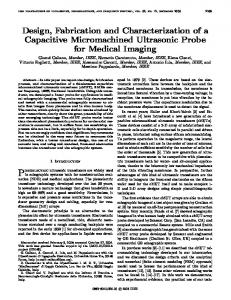
as PMRTC [5]. In Fig. 1 the circuit diagram of a PMRTC is shown. The secondary side of the transformer is connected to a half bridge high frequency rectifier. Here, D1 , D2 , D3 and D4 are the body diodes and C1 , C2 , C3 and C4 are the body capacitances of the switches used (MOSFETs / IGBTs). The gate pulses (vgs ) of the devices are shown in Fig. 2.
Keywords—Phase Modulated Resonant Transition Converter, ZVS, Resonant Converter, Phase Modulation, High Frequency Welding Converters.
I.
I NTRODUCTION
PMRTC is a full bridge isolated DC to DC converter, operating under Zero-Voltage-Switching (ZVS) principle along with phase modulation of the gate pulses of the switches [1], [6]. This configuration offers the voltage-current characteristics required for welding applications and serves to bring down the apparatus size to that of a small portable unit, unlike the conventional large welding units [2]. Modern TIG welding machines generally utilise switched mode DC/DC power supplies which provide high DC current at low DC arc voltages at the output. Switched mode DC/DC power supplies can be operated at high switching frequencies due to the advancement in semiconductor technology providing fast switching with small rise and fall times yielding high frequency operation with low loss. The advantage of using high switching frequency in electrical circuits is that the size of the circuit elements like inductors, transformers, capacitors etc. get reduced. At these power levels and the high switching frequency involved, switching losses are a major concern. These losses can be minimised by using soft switching(as switching loss directly proportional to switching frequency) [3]. Soft switching are of two types. Zero current switching(ZCS) and Zero voltage switching(ZVS). The circuit under consideration can be operated either in ZCS or ZVS. The output capacitances of the switches can be utilized for ZVS operation [1]. The output voltage at the load terminal is controlled by means of phase shifting (0o − 180o ) the pulses of the diagonal pair switches of the inverter [4]. There must be a dead time(td ) between the pulses of the same leg switches(to avoid shoot through). The selection of td , resonating elements (transformer leakage inductance and device parasitic capacitances)and the phase shift are done such that resonance occurs within the dead time. Whenever the full bridge DC/DC converter is operated under phase shift PWM with resonance method, it is called
978-1-4799-6373-7/14/$31.00 ©2014 IEEE
Fig. 1.
Circuit diagram of PMRTC
Fig. 2.
Gate to Source voltage (vgs ) of the devices
II.
O PERATING
PRINCIPLE OF
PMRTC
The complete operation of the converter can be divided into ten distinct modes (5 in each half cycle) [1], [4], [7]. Representative waveforms of the steady state primary voltage (vp ), secondary voltage (vs ) and primary current (ipri ) are shown in Fig.3 [4]. Since the secondary current (isec ) is the scaled version of ipri , it is not separately included in the figure.
Fig. 5.
Fig. 3. Theoretical waveforms of ipri , vp and vs in a complete cycle operation of PMRTC
MODE 0 In this mode switch S3 and S4 are conducting and the power is transferred from source to load. Let at the starting of this mode the value of ipri be +Ip (0). In Fig. 4 the current conduction path is shown [5].
Circuit configuration when PMRTC is operating in mode 1
of this mode). So, it will obviously flow through C1 and C4 [5]. As a result vC1 (which was at Vdc at the beginning of mode 1) falls to zero and vC4 (which was at zero voltage at the beginning of mode 1, as S4 was on) reaches Vdc . This charging and discharging can be considered linear as the charging and discharging is accomplished by the stored energy of the output filter inductor. At the end of mode 1 vC4 = Vdc and vC1 = 0. As soon as vC1 (which is also primary voltage (vp )) reaches zero, D1 gets forward biased and start conducting and mode 2 begins. S1 can be turned on beyond this point with zero voltage across it. At the end of mode 1: vp = 0 , vs = 0 [5]. Mode 2 In this mode ip freewheels through S3 and D1 . vp & vs remains zero. At the end of this mode ip decreases to ′
+Ip2, as shown in Fig. 3, with a slope as soon as S3 is turned off.
−V0 Leq
. Mode 3 begins
Mode 3
Fig. 4.
As soon as S3 is turned off, ip flows through C2 and C3 (as it cannot flow through D2 because of the same reason stated in mode 1). As a result C3 starts charging and C2 starts discharging. The circuit configuration at the starting of mode 3 is shown in Fig. 6. Now as soon as the voltage
Circuit configuration when PMRTC is operating in mode 0 ′
′
V0 is the output DC voltage referred to primary. If L0 is the output filter inductance referred to primary, LLK1 ′ is the primary leakage inductance, LLK2 is the secondary leakage inductance referred to primary and Lm is the magnetizing inductance of the transformer, then it can be shown that the equivalent inductance referred to primary is ′ ′ ((L0 + LLK2 ) k Lm ) + LLK1 [5]. As Lm is large, this parallel branch can be neglected. The equivalent inductance (Leq ) ′ ′ (referred to primary) becomes Leq = L0 + LLK2 + LLK1 . (V
′
−V )
So, ipri rises with a slope dcLeq 0 and reaches +Ip(max) at the end of this mode (where Vdc is the input DC voltage). Mode 0 ends as soon as S4 is switched off and mode 1 starts [5]. Mode 1 Mode 1 persists for a very short time. The circuit configuration is shown in Fig. 5. As soon as S4 is switched off, ipri will not be able to flow through D1 as it is reversed biased by the voltage across capacitor C1 (which is Vdc at the starting
Fig. 6.
Circuit configuration at the beginning of mode 3
across C3 becomes grater than the total leakage inductance drop and primary referred forward voltage drop of the diode D6 , D6 gets forward biased and starts conducting. The circuit configuration in this mode is shown in Fig. 7 [5]. vs remains zero as both the secondary side rectifier diodes (D5 & D6 ) are conducting while the primary voltage(which is also −vC3 ) reaches −Vdc at the end of this mode. Now as soon as D6
Fig. 8. Fig. 7.
Circuit configuration for t3 > t > t2 in mode 4
Circuit configuration in mode 3 after D6 is turned on
starts conducting, the charging of C3 and discharging of C2 is sustained by the stored energy in the leakage inductance of ′ the transformer only (As L0 plays no role) [5].
[5]. D5 commutates at t4 and next half cycle begins. The rest
vC2 falls from Vdc to zero within this mode. It can be shown that, to satisfy ZVS, ELK > ECt or, Fig. 9.
1 1 2 2 L(Ip 2) > Ct (Vdc ) 2 2 where Ct = C2 + C3 .
of the circuit operations are identical with reverse polarity for the next half cycle.
There will be resonant action between LLK and Ct .
III.
The resonant frequency is,
Tr =
A NALYSIS
OF
PMRTC
Zero voltage switching condition
1 √ fr = 2π LLK Ct So, resonant period,
Circuit configuration for t3 < t < t4 in mode 4
(1)
(2)
1 ωr
(3) th
vp = −vC3 reaches from zero to −Vdc within 14 of Tr . To achieve ZVS, Tr td ≥ (4) 4 Substituting (2) & (3) in (4) we get, πp td ≥ LLK Ct (5) 2 As soon as voltage across C2 reaches zero, D2 starts conducting and mode 4 starts. S2 can be turned ON beyond this point with zero voltage across it. Mode 4 The circuit configuration at the starting of mode 4 (t3 > t > t2 corresponding to Fig. 3) is shown in Fig. 8 [5]. The transformer dc primary current starts to decrease rapidly with a slope −V LLK . The secondary voltage is still zero as both the rectifier diodes are conducting. Now, at t3 diode D1 and D2 commutates and S1 and S2 starts conducting. The current increases with the same slope and reaches −Ip(0) at t4 (as shown in Fig. 3). The circuit configuration for t3 < t < t4 is shown in Fig. 9
It is seen from the previous discussion that capacitor C1 and C4 discharged and charged (or vice-versa for the next half cycle) under the influence of stored energy in the output filter inductor. So, ZVS is satisfied even at a very light load. In case of C2 and C3 the charging and discharging operation is accomplished by the stored energy in the leakage inductance only. So, there is a critical value for +Ip2 at the starting of mode 3 (−Ip2 for mode 8 in the next half cycle), below which ZVS is not satisfied. The critical value for Ip2 (Ip2cr ) is dictated by r Ct Ip2cr = Vdc (6) LLK ′
where, LLK = LLK 1 + LLK2 + Ladd (additional series inductance, if used) [4]. It can be shown that, Ip2 =
1 ∆I0 V0 Ts (I0 + − (1 − d0cri ) ) n 2 L0 2
(7)
where, d0cri is the critical value of d0 (shown in Fig. 2) for which ZVS is satisfied. Input to output DC voltage relation is 1 (8) V0 = ( )d0ef f Vdc n where d0ef f is the ratio of total duration of voltage appearing across the transformer secondary to the switching time period (Ts ) [4].
IV.
D ESIGN
OF
There is 2µs dead time between vgs of same leg switches.
PMRTC
The design has been done on the basis of the condition stated in the previous sections. The transformer is designed for larger VA rating for possible increase of current rating in future. The transformer wire gauge is chosen such as to minimise skin effect at 50kHz. Ladd , is added in series with the primary winding, as leakage inductance was not sufficient to achieve ZVS for very low load current. Design specifications are enlisted in Table I Item Transformer
Design Parameter VA n Core LLK1
Series inductance Switching frequency Output inductor Output capacitor Input voltage Output current Load resistance Output voltage Dead time (each leg) Phase shift MOSFET (IRF640)
TABLE I.
V.
LLK2upperhalf LLK2lowerhalf Lm rp rs (both half) Wire gauge (both half) Ladd fsw L0 C0 Vdc I0 R0 V0 td φs Cds
Value 2191 5 ET D59/31/22Fig. 11. Simulated waveforms: vp , vs , ipri , (Scale: t : 10µSec/div, v : 7.08µH 10V /div, fsw : 50kHz) 140nH 140nH Fig. 11 shows that simulated waveforms of vp , vs and ipri . 5.15mH 50mΩ 0.7mΩ SWG 24 727.2µH 50kHz 200µH 200µF 30V 0.4A 0.2Ω 80mV 2µS 60 deg 12. Simulated waveforms: vLadd , (Scale: t : 10µSec/div, v : 10V /div, 160pF Fig. f : 50kHz)
S PECIFICATIONS OF DIFFERENT CIRCUIT ELEMENTS OF PMRTC
S IMULATED
sw
In Fig. 12 simulated voltage across additional inductance (vLadd ), is shown. It varies from +30V to −30V . It can be observed that there is a significant amount of voltage drop across Ladd , which effectively decreases the amount of active power transfer to the output load.
AND EXPERIMENTAL RESULTS
A. Simulated results for an idealised model The total circuit is simulated off-line using SEQUEL.
Fig. 13. Simulated waveforms: id5 , id6 , (Scale: t : 5µSec/div, v : 100mA/div, fsw : 50kHz) Fig. 10. Simulated waveforms of the gate pulses: vgs3 , vgs1 , vgs2 , vgs4 , (Scale: t : 5µSec/div, y : 10V /div , fsw : 50kHz)
Fig. 10 shows simulated vgs of the devices. vgs of the diagonal pair switches are phase shifted with respect to each other.
In Fig. 13 the transformer secondary diode currents are shown. In the simulation stated above, the effect of transformer interturn capacitances were neglected. When the inter-turn capacitances are considered, the waveforms are different than the
theoretically predicted ones (at 50kHz inter-turn capacitances of the transformer windings having considerable effect). B. Comparison of results for a more exact model In the following simulation, transformer inter-turn capacitances are considered. It is seen from Fig.14 & 15 that the
Fig. 17. Experimental waveforms: vp , vLadd , (Scale: t : 2.5µ sec/div, yvL : 25 V/div, yvp : 10 V/div, fsw : 50kHz) add
Fig. 14. Simulated waveforms: vgs3 , vgs1 , vgs2 , vgs4 , (Scale: t : 5µSec/div, v : 10V /div , fsw : 50kHz)
Fig. 18. Simulated waveforms: vinv ,ipri , (Scale: t : 10µ sec/div, ylef t : 10 V/div, yright : 50 mA/div, fsw : 50kHz)
Fig. 15. Experimental waveforms: vgs3 , vgs1 ,vgs2 , vgs4 , (Scale: t : 10µ sec/div, y : 20 V/div, fsw : 50kHz)
practical vgs exactly matches with the simulated result.
Fig. 16. Simulated waveforms: vp , vLadd , (Scale: t : 5µ sec/div, y : 20 V/div, fsw : 50kHz)
Similarly we see from Fig.16 & 17 that the practical results of vp & vLadd are in excellent correlation with the simulated ones. It is seen from Fig. 19 that the primary current reaches maximum value 120mA. Fig. 18 shows its simulated value is 125mA, hence they are in excellent correlation. It is seen from Fig. 20 & 21 that the gate pulse is applied after the voltage across the device falls to zero. In the current waveform there are spikes, which appear due to delay in turn-on of the MOSFET’s body diode.
Fig. 19. Experimental waveforms: ipri , vinv , (Scale: t : 5µ sec/div, yvinv : 10 V/div, yipri : 100 mV/div, Hall sensor gain 0.78 A/Volt, fsw : 50kHz)
Fig. 20. Simulated waveforms: vgs3 ,vds3 , ids3 (Scale: t : 5µ sec/div, ylef t : 5 V/div, yright : 50 mA/div, fsw : 50kHz)
Experimental Set-up Fig. 22 shows a photograph of the experimental set-up of PMRTC. In Fig. 23 the photograph of the control circuits is shown. VI.
C ONCLUSIONS
In this paper the operating principle, design, fabrication and off-line simulation using SEQUEL (for ideal case and also for the practical case) of a PMRTC has been presented. Thereafter
[5] [6]
[7]
Fig. 21. Experimental waveforms: vgs3 , vds3 , ids3 (Scale: t : 2.5µ sec/div, yvds3 : 10 V/div, yvgs3 : 10 V/div, yids : 100 mV/div, Hall sensor gain 3 0.78 A/Volt, fsw : 50kHz)
Fig. 22.
Experimental Set-up of PMRTC (power circuit)
Fig. 23.
Experimental Set-up of PMRTC (control circuit)
the converter has been fabricated and tested with 50kHz, 30V(dc-link) for a load of 0.2Ω. The experimental results are in excellent correlation with the simulated (considering interturn capacitances) ones. VII.
ACKNOWLEDGEMENTS
The authors would like to express their gratitude for the fund support received from the NaMPET initiative of the Govt. of India, DIT, MCIT. The assistance received from the research colleagues particularly, Mr. P. Mukherjee & Mr.N.Dutta, at the Advanced Power Electronics Laboratory,Dept. of E.E.,IIEST are also thankfully acknowledged. The authors also acknowledge the support received from the authorities, IIEST, Shibpur, Howrah towards this work. R EFERENCES [1] [2] [3] [4]
Ramanarayanan V ’Course material on switched mode power conversion’, IISC Bangalore, March 27, 2007. Mukherjee Pinaki ”Power electronic converters for welding applications”, M.E thesis of 2011-2012. Krein. P.T, ”Elements of power electronics”, New York, Oxford,1998. J. A. Stable, V. Vlatkovic, R. B. Ridley, F. C. Lee, and B. H. Cho, ’Design considerations for high-voltagee high-power full-bridge zerovoltage switched PWM converter’, Applied Power Electronics Conference Proceedings, pp. 275-284, 1990.
Kar Abhishek ”Power electronic converters for welding and other HF applications”, M.E thesis of 2013-2014. Mukherjee P, Sengupta M ’Fabrication, Simulation and Testing of a ZeroVoltage-Switching Strategy based High Frequency Buck Chopper’, IEEE Conference, PEDES-2012. Mukherjee P, Sengupta M ’Design, Fabrication and Testing of a Current Controller for a Phase Modulated Full Brirge Isolated Step Down DC/DC Converter’, NPEC Conference 2013.