Design of Injected Grid Current Regulator and Capacitor-Current-Feedback Active-Damping for LCL-Type Grid-Connected Inverter Chenlei Bao, Xinbo Ruan, Xuehua Wang, Weiwei Li, Donghua Pan, and Kailei Weng State Key Laboratory of Advanced Electromagnetic Engineering and Technology Huazhong University of Science and Technology Wuhan, P. R. China
[email protected] and
[email protected] resonance of the LCL filter requires proper damping methods, otherwise the system might go unstable [3], [4].
Abstract—The injected grid current regulator and active damping of the LCL filter are essential to the control of LCL-type grid-connected inverters. Generally speaking, the current regulator guarantees the quality of the injected grid current, and the active damping reduces the resonance peak caused by the LCL filter and makes it easier to stabilize the whole system. However, the frequency responses of the current regulator and active damping interact with each other, making it difficult to design the proper controller parameters and investigate the effect of the controller parameters. Taking proportional-integral (PI) compensator together with capacitor-current-feedback active-damping as an instance, this paper proposes a step-by-step design method of the current regulator and capacitor current feedback coefficient in both analog control and digital control. By carefully dealing with the interaction between the current regulator and active damping, the satisfactory regions of the controller parameters are obtained based on stability margin and steady-state error checking, making it more convenient and explicit to optimize the performance of the system. The convenient trial-and-error procedures are successfully reduced. Experimental results verify the effectiveness of the proposed design method.
A direct way to damp this resonance is introducing a passive resistor into the filter circuit, which is called passive-damping method [5], [6]. The addition of a resistor in series with the filter capacitor has been widely adopted for its simplicity and relatively low power loss, but the ability of attenuating the switching harmonics is weakened. A resistor added in parallel with the filter capacitor does not impair characteristics of the LCL filter in both low- and high-frequencies, but power lose of the damping resistor can not be accept [7].
I. INTRODUCTION Nowadays, distributed power generation systems (DPGSs) based on renewable energy sources have drawn more and more attention for its environmental friendly features. Grid-connected inverters injecting high-quality power into the grid play important roles in DPGSs [1]. In order to attenuate the switching frequency harmonics produced by pulse-width modulation (PWM) of the grid-connected inverters, L and LCL filters are usually introduced. Compared with the L filter, the LCL filter has an additional capacitor branch bypassing high-order harmonics, yielding a better switching frequency harmonics attenuation. As a consequence, under the same harmonics suppression requirements, the LCL filter offers a better choice for its reduced volume and cost [2]. However, the inherent This work was supported by the National Natural Science Foundation of China under Award 50837003 and Award 51007027, and the National Basic Research Program of China under Award 2009CB219706.
978-1-4673-0803-8/12/$31.00 ©2012 IEEE
579
Thus the virtual resistor is proposed in replace of the passive resistor, which is called an active-damping method. The feedback of voltage or current of the filter components is used to damp the resonance oscillation, and the extra power losses are successfully avoided. In Ref. [8], the concept of “virtual resistor” was proposed based on equivalent transformations of the LCL-type grid-connected inverter mathematical model. It was pointed out that active damping based on proportional capacitor current feedback was equivalent with a resistor in parallel with the filter capacitor. In this paper, this active-damping method is adopted for its simplicity. Nevertheless, the resonance oscillation can not be effectively damped if the feedback coefficient is too small, and the phase margin will be enormously reduced if the feedback coefficient is too large. So the choice of the capacitor current feedback coefficient is critical [9] [10]. Besides, PR compensator and PI compensator are widely used to control the injected grid current in single-phase grid-connected inverters. PR compensator can provide infinite gain at the selected resonant frequency to eliminate steady-state error or to suppress unwanted har monics. Compared with PR compensator, PI compensator suppresses the dc injected grid current, but the
vg(s) iref (s)+ –
Gi(s) +
– 1 +– 1 Ginv + sC sL1 –
+– 1 sL2
ig(s)
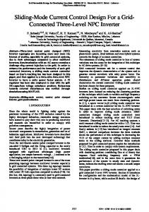
Hi1 Hi2 (a) (b) Figure 1. An LCL-type single-phase grid-connected inverter based on filter-capacitor-current-feedback active damping. (a) Topology and control block. (b) Block diagram in the analog control.
zero steady-state error of the injected grid current can not be achieved [9]. When the grid voltage feed-forward scheme is adopted, PI compensator is competent for the regulation of the injected grid current [11] [12]. Design method based on PI compensator is discussed for instance in this paper.
iref ( s)
Traditionally, root locus [9], dominate poles placement [10] and bode diagram [13] are introduced to design the injected grid current regulator together with the capacitor-current-feedback active-damping in the LCL-type grid-connected inverter. Massive trial-and-error procedures are usually necessary to get proper controller parameters with the aforementioned design methods. And there is little literature mentioning the effects and optimal choices of the current regulator together with capacitor current feedback coefficient considering the interaction of the controller parameters.
Figure 2. Equivalent block diagram of Fig.1(b).
and the injected grid current sensor. Gi(s) is the injected grid current regulator. The feedback of capacitor current is used for active damping, Hi1 is the feedback coefficient. Unipolar sinusoidal pulse width modulation (SPWM) is used here. The resonance frequency fr is derived as fr =
1 2π
L1 + L2 L1L2C
(1)
The ASM shown in Fig. 1(b) can be transformed into the model depicted in Fig. 2 using the same simplifying procedure presented in [12]. The expressions of Gx1(s) and Gx2(s) are given by GinvGi ( s ) Gx1 ( s ) = 2 (2) s L1C + sCGinv H i1 + 1
This paper investigates the design method of the injected grid current regulator and capacitor-current-feedback activedamping for the LCL-type single-phase grid-connected inverter. In Section II, the grid-connected inverter is modeled using average switching model (ASM). Taking the PI-based current regulator as an instance, the effects of the controller parameters on the phase margin, gain margin and steady-state error are investigated in Section III. And a step-by-step design method of the controller parameters is proposed to meet the aforementioned specifications. In Section IV, according to Nyquist stability criterion, the design method is extended to the system in the digital control. A design example is presented in Section V. The effectiveness of the proposed design method is verified by the experimental results from a 6-kW prototype in Section VI. And the conclusion is given in Section VII.
Gx 2 ( s ) =
s 2 L1C + sCGinv H i1 + 1 s 3 L1L2C + s 2 L2CH i1Ginv + s ( L1 + L2 )
(3)
where Ginv=Vin/Vtri is the transfer function of the inverter bridge, and Vtri is the amplitude of the triangle carrier wave. Thus the injected grid current ig can be derived as ig ( s ) =
1 T (s) G (s) ⋅ ⋅ iref ( s ) − x 2 ⋅ vg ( s ) H i 2 1 + T (s) 1 + T (s)
(4)
= ig 1 ( s ) + ig 2 ( s )
where T(s) is the loop gain of the system and is expressed as
II. MODELING THE GRID-CONNECTED INVERTER
T (s) =
Fig. 1 shows the topology and control scheme of an LCL-type single-phase grid-connected inverter. The LCL filter is composed of L1 , C, and L2, where L 1 is the inverter-side inductor, C is the filter capacitor, and L2 is the grid-side inductor. The equivalent series resistors of L1, C, and L2 are relatively small and ignored here. Vin is the dc-link voltage, vinv is the output voltage of the inverter bridge. Hv and Hi2 are the gains of the grid voltage sensor
H i 2GinvGi ( s ) s 3 L1L2C + s 2 L2CH i1Ginv + s ( L1 + L2 )
(5)
ig1 is related to the injected grid current reference iref, and ig2 is related to the grid voltage vg. ig1 and ig2 are expressed as 1 T ( s) ⋅ ⋅ iref ( s ) H i 2 1 + T (s) G ( s) ig 2 ( s ) = − x 2 ⋅ vg ( s ) . 1 + T ( s)
ig 1 ( s ) =
580
(6) (7)
Figure 4. Phasor diagram of the grid voltage and injected grid current
The steady-state error of ig consists of two parts: phase error δ and amplitude error EA. According to (6) and (7), δ can be calculated as ig 2 ( j 2π f o ) H i 2 Gx 2 ( j 2π f o ) ⋅ Vg = tan δ = (11) ig1 ( j 2π f o ) T ( j 2π f o ) ⋅ I ref where Vg is the root-mean-square (RMS) value of the grid voltage, and Iref is RMS value of the reference. Similar to the approximation used in (8), Gx2(s) is approximated to 1/[s(L1+L2)] in magnitude at fc and the frequencies lower than fc. Substituting this and (8) into (11), δ is derived as
Figure 3. Bode diagram of the loop gain without compensation.
III. DESIGN OF CURRENT REGULATOR AND CAPACITOR CURRENT FEEDBACK COEFFICIENT IN ANALOG CONTROL A step-by-step design method of controller parameters is proposed in this section by examining the phase margin (PM), gain margin (GM) and steady-state error. For the convenience of derivation, it is assumed the inverter is controlled to inject active power only.
T fo = 20lg T ( j 2π f o ) = 20lg
According to Fig. 4, EA can be calculated as H i 2ig ( j 2π f o ) − I ref H i 2 ig1 ( j 2π f o ) cos δ
EA =
According to (5), bode diagram of the uncompensated loop gain with different Hi1 is shown in Fig. 3. As seen, a larger Hi1 leads to a better damped resonant peak but a more decreased phase margin. As the crossover frequency fc is usually set lower than 1/10 equivalent switching frequency considering the effect of attenuating high-frequency noise [7], and fr is usually designed in the region from 1/4 to 1/2 equivalent switching frequency to ensure effective harmonics suppression and well dynamic response. Thus the capacitor’s influence can be ignored and T(s) can be approximated in magnitude as follows at fc and the frequencies lower than fc: H i 2GinvGi ( s ) . s ( L1 + L2 ) Ki . s
=
I ref
I ref
−1
(13)
Substituting (6) into (13), EA is obtained as T ( j 2π f o ) 1 1 EA = −1 ≈ −1 . (14) 1 + T ( j 2π f o ) cos δ cos δ Eq. (14) can be further rewritten as cosδ≈1/(1+EA). It is apparent that, EA is related to δ. In fact, the power factor (PF) of the inverter defined as cosδ is also important. Thus, the lower boundary of cosδ is determined as max{PF, 1/(1+EA)}. Thus, the steady-state error is united as δ. According to (12), the steady-state error can be further specified by Tfo. According to (8) and (9), Tfo is expressed as
(8)
T fo = 20lg T ( j 2π f o ) = 20lg
The transfer function of PI compensator is given by Gi ( s ) = K p +
(12)
where the unit of Tfo is dB.
A. Controller Parameters Constrained by Steady-State Error and Stability Margin
T ( s) ≈
H i 2Vg
2π f o ( L1 + L2 ) I ref tan δ
(9)
At the frequencies around the transition frequency of Gi(s) fL (fL=Ki/(2πKp)), the slope of the magnitude curve changes from −20 dB/dec to 0 dB/dec and the phase shift changes from −90° to 0°. As the negative phase shift of Gi(s) impacts phase margin, fL is suggested to be set much lower than fc. Thus, Gi(s) can be approximated to Kp in magnitude at fc and the frequencies higher than fc. As |T(j2πfc)|=1, according to (8), the relation between Kp and fc is given by 2π f c ( L1 + L2 ) . Kp ≈ (10) H i 2Ginv
As shown in (4), the injected grid current ig consists of ig1 and ig2. The phase of iref is the same as vg. And when the magnitude gain at fundamental frequency Tfo is large enough, ig1 tracks iref well. As a result, the phase of ig1 is approximately the same with vg and the phase of ig2 is 90º lag to vg considering the direction of ig defined as flowing into the grid [11]. The phasor diagram is depicted in Fig. 4.
j 2π f o ( L1 + L2 )
.
(15)
Substitution of (10) into (15) leads to 2 4π 2 f o ( L1 + L2 ) T 20 Ki =
H i 2Ginv
(10
f o ) − f c2 .
fo
(16)
According to (5), the PM of the system is expressed as PM = 180D − ∠
H i 2GinvGi ( s) s 3 L1L2C + s 2 L2CH i1Ginv + s ( L1 + L2 ) s = j 2π f
Substituting (9) into (17), leads to 2π L1 ( f r2 − f c2 ) PM = arctan
− arctan
H i1Ginv f c
(17) c
Ki . 2π f c K p
Eq. (18) can be rewritten as 2π L1 ( f r2 − f c2 ) − Ginv f c H i1 tan PM . K i = 2π f c K p 2π L1 ( f r2 − f c2 ) tan PM + Ginv f c H i1 Substitution of (10) and (16) into (19), leads to H i1 =
(10 f ) − f tan PM ) tan PM + f (10 f ) −f )
(
2π L1 ( f r2 − f c2 ) f c2 − f o
(
Ginv f c f c2
581
H i 2Ginv ( K p + Ki j 2π f o )
2
T fo 20
2 c
o
2
T fo 20
o
o
2 c
(18)
(19)
(20)
0.20
modify the specifications and do Step (2) again.
Hi1
Restriction by 0.15 PM and Tfo
Step (3)
For a specific fc, calculate the lower and upper boundaries of Hi1 from (22) and (20), respectively, and Hi1 can be picked out from this region.
Step (4)
After fc and Hi1 have been determined, calculate the lower and upper boundaries of Ki from (16) and (19). Then choose Ki from this region by trading off between the Tfo and PM.
Step (5)
Check the compensated system to ensure that it satisfies all the specifications.
0.10
GM = 3dB PM = 45° Restriction Tfo = 52dB by GM 0 0.5 1.0 3.0 1.5 2.0 2.5 fc (kHz) Figure 5. The constrained region of fc and Hi1 in the analog control. 0.05
TABLE I: System Parameters Dc-link voltage Grid voltage (RMS) Fundamental frequency
Vin
360 V
Inverter-side inductor
L1
600 μH
Vg
220 V
Filter capacitor
C
10 μF
L2
150 μH
fr
4.6 kHz
Vtri
3V
Hi2
0.15
fo
50 Hz
Output power
Po
6 kW
Switching frequency
fsw
10 kHz
Sampling frequency
fs
∞ 20 kHz
Grid-side inductor Resonance frequency Amplitude of the carrier wave Injected grid current feedback coefficient
The GM is defined as the magnitude at fr, i.e., GM = −20lg T ( j 2π f r ) where the unit of GM is dB. Substituting (5) and |Gi(s)|≈Kp into (21), leads to 2π f c L1 . H i1 = 10GM 20 ⋅ Ginv
B.
From the design procedure proposed above, it is noticed that, with the regions of the controller parameters obtained, after fc is confirmed, the parameters can be optimized according to different requirements: 1) a larger Ki can be chosen for larger Tfo; 2) a larger Hi1 can be chosen for larger GM; 3) a smaller Ki and Hi1 can be chosen for larger PM. IV. DESIGN IN DIGITAL CONTROL In practice, the digital control is widely used in the grid-connected inverters for its flexibility and simple external circuitry. However, the inherent discrete nature of PWM systems and digital controllers usually can not be ignored, especially when the switching frequency is low. It is necessary to investigate the design in the digital control.
(21)
A.
The ASM of the LCL-type grid-connected inverter in the digital control is shown in Fig. 6. As the presence of the sampling and computation delays, the voltage command is usually held and loaded at the next period. Thus, one period computation delay z-1 is usually considered (the sampling delay is included). And in order to accurately model the behavior of the PWM pattern generator, the zero-order hold (ZOH) method is introduced. ZOH is given by (1-e−sTs)/s, where Ts=1/fs is the sampling time. Backward difference is used for discretizing PI compensator Gi(z). Thus the injected grid current ig in the digital control can be derived as
(22)
Design Procedure of Controller Parameters
Based on (20) and (22), the relationship between Hi1 and fc can be obtained as shown in Fig. 5 (parameters are listed in TABLE I). The area upon the dashed line meets GM>3 dB, the area under the solid line meets the PM>45º and Tfo>52 dB. The shaded area includes all the possible parameters satisfying the specifications. According to this satisfactory region, the design procedure turns to be convenient and explicit, and is shown as follows: Step (1)
Step (2)
ig ( s ) =
Determine the specifications of the loop gain, i.e., including Tfo by the requirement of the steady-state error, GM by the requirement of the robustness, and PM by the requirements of the dynamic response and robustness, respectively.
G ( z) 1 T ( z) ⋅ z ⋅ iref ( z ) − x 2 _ z ⋅ vg ( z ) H i 2 1 + Tz ( z ) 1 + Tz ( z )
(23)
where Tz(s) is the loop gain and is expressed as (24) in the bottom, and ωr=2πfr. B.
Open-Loop Unstable Poles and Nyquist Criterion
Because of the delay caused by the computation and PWM pattern generator, the system is no longer a min-phase system [14]. Open-loop zeros or even poles may be outside the unit circle, affecting the system performances. Thus it is necessary to analyze whether open-loop unstable poles exist. As Gi(z) is discretized by backward difference, no open-loop unstable poles exist. If Den(z) expressed in (25) has no open-loop unstable poles, Tz(z) will not have as well.
Draw the region constrained by the specifications aforementioned, as depicted in Fig. 5. Determine the appropriate fc with the compromise of the dynamic response and attenuation ability of highfrequency noise. Then calculate Kp from (10). Specially, if the specifications are too strict, the region may be too small or even not exist, then Tz ( z ) =
Modeling the Inverter in Discrete-Time Domain
⎡Tsωr ( z 2 − 2 z cos ωrTs + 1) − ( z − 1)2 sin ωrTs ⎤ Gi ( z ) H i 2Ginv ⎣ ⎦ . ( L2 + L1 )ωr ( z − 1) ⎡ z ( z 2 − 2 z cos ω T + 1) + H i1Ginv L2C ⋅ ( z − 1)ω sin ω T ⎤ r s r r s ⎢ ⎥ L2 + L1 ⎣ ⎦
582
(24)
iref (z) +
Gi(z)
_
+ _
z-1
ZOH
Ginv
+
_
_
+
1 sL1
1 sC
+
vg(s) _
ig(s)
1 sL2
ig(z)
Hi1 Hi2
Den( z ) = z 3 − 2 z 2 cos ωrTs + z +
H i1Ginv L2Cωr ( z − 1) sin ωrTs L2 + L1
|Tz(j2pf)| (dB)
Figure 6. The ASM of inverter in digital control.
(25)
H i1Ginv L2Cωr sin ωrTs ⎧ ⎪ a0 = 1 + cos ωrTs + L2 + L1 ⎪ H G L2Cωr sin ωrTs i 1 inv ⎪⎪ a1 = 1 + cos ωrTs − 2 . ⎨ L2 + L1 ⎪ H i1Ginv L2Cωr sin ωrTs ⎪ a2 = 1 − cos ωrTs + L2 + L1 ⎪ ⎪⎩ a3 = 1 − cos ωrTs
|Tz(j2pf)| (dB)
1− w
where
(27)
∠Tz(j2pf) (deg)
According to Routh’s Method, if no open-loop unstable poles exit, the following conditions must be satisfied: ai≥0 (i=0,1,2,3), b1≥0 (b1=(a1a2−a0a3)/a1).
Ginv L2Cωr sin ωrTs
i1
≤
( 2cos ωrTs − 1) ( L2 + L1 ) . Ginv L2Cωr sin ωrTs
Kp decreases
GM1 PM
-180
-540
fr
fc Freuqency (a)
GM2 0
Kp decreases
GM1 PM
-180
The sampling frequency fs must be larger than 2fr to ensure the inverter is controllable [15], i.e., ωrTs0 is investigated in this paper). And the quantity of the unstable poles equals to the quantity of sign changes of the first column elements in Routh’s array. So there are two unstable poles if Hi1 does not meet (28). As well known, PM and GM are usually adopted to describe the stability margin as analyzed in Section III. But it maybe not enough if the system is a non-min-phase system. Nyquist stability criterion tells that, a system is stable only if the number of anticlockwise encirclements of the critical point (−1, 0j) equals to the number of the open-loop unstable poles plus clockwise encirclements of the critical point. Thus, corresponding to the bode diagram, a system is stable only if the number of the positive crossing −180º minus negative crossing −180º equals to half of the open-loop unstable poles. Specially, in this case, it can be proved that, the phase curve passes across −180º at fr, and if Hi1 does not satisfy (28) the curve also passes across −180º at fs/6 (neglect the effect of Gi(z) on the phase at fr and fs/6). The detail proof is presented in Appendix. Thus,
2. When Hi1 does not satisfy (28), the bode diagram is depicted in Fig. 7(b). Because of the two open-loop unstable poles, the phase increases near the unstable poles corresponding frequency, thus the phase curve will pass through −180º twice, and f1=min{fr, fs/6}, f2=max{fr, fs/6}. Thus, the dash line introduces one time negative crossing at f1 and one time positive crossing at f2, leading to an unstable system. The dash-and-dot line does not introduce any negative crossing or positive crossing, and the system is also unstable. The solid line introducing once positive crossing at f2 is the only possibility leading to a stable system. Thus, in order to ensure the stability, the magnitude must be lower than 0 dB at f1 and larger than 0 dB at f2.
583
C.
0.06
Controller Constraints in Discrete-Time Domain
Since analyzing the loop gain with (24) is too complex and unclear, the model in frequency domain is introduced to help to analyze [16]. In frequency domain, Gi(z) can be approximated as Gi(s). The sampler is approximated as 1/Ts under the Nyquist frequency fs/2. The computation delay is expressed as e-sTs, and ZOH is rewritten as e jωTs / 2 − e − jωTs / 2 − jωTs / 2 Gh ( jω ) = e ≈ Ts e − jωTs / 2 . jω
0.04 Hi1
0.5
Ginv
2
2
(32)
where the unit of GM1 and GM2 are dB, GM1>0 and GM2>0 mean the magnitude lower than 0 dB at those frequencies. It is noticed that, the current regulator Gi(z) may shift the frequencies where the phase curve passes through −180º. Thanks to GM1 and GM2, the tiny frequency shift can be approached as the robustness of the system, and is unnecessary to be considered.
Taking the inverter in the digital control as an instance, controller design of the PI-based injected grid current regulator and capacitor-current-feedback active-damping is proposed in this section, the parameters of the inverter are listed in TABLE I. The design procedure is as follows: 1) Determine the specifications of the loop gain. PM>20° and GM13 dB ensure well dynamic response and enough stability margin (in this case fs/652 dB ensures PF greater than 0.98 when output power is larger than 50% of the rated power [17].
Design of Controller in Discrete-Time Domain
As analyzed in Section IV-B, different value of fs may lead to different stability conditions.
2) Obtain the region of Hi1 and fc satisfied all the requirements according to (31), (32) and (35), as depicted in Fig. 8. fc=1.5 kHz is chosen to obtain fast dynamic response. Then Kp=0.3 is calculated according to (10).
1. if fs/6≤fr, for stability, the magnitude of the loop gain at fs/6 must be lower than 0 dB and at fr must be larger than 0 dB, i.e., GM10 dB.
π
Ki PM = − 3π f cTs − arctan − arctan 2 2π f c K p K i = 2π f c K p
H i1 =
(10
T fo 20
2.5
V. DESIGN IN DIGITAL CONTROL
The PM is confirmed by PWM and computation delay, current regulator and active damping, given by (33). Ki and Hi1 constrained by the PM are given by (34) and (35), respectively. These are expressed in the bottom of this page. D.
2.0
Therefore, the design procedure proposed in Section III-B can be extended to that in the digital control. According to (31), (32) and (35), the satisfactory region of Hi1 and fc can be obtained as the shaded area in Fig. 8 (parameters are listed in TABLE I). Then all the possible parameters can be determined easily according to the proposed design method. As the negative phase shift introduced by the delay, the PM determined in the first step may not be set too large. And the boundaries of Hi1 are constrained by GM1, GM2 and PM in the digital control.
1
⎛ 6 f r ⎞ 2π L1 f c 2π L1 ( f s 6 ) − ( f r ) + ⎜ f ⎟ G Ginv fs 6 inv ⎝ s ⎠
1.5 fc (kHz)
2. if fs/6>fr, when Hi1 satisfies (28), the magnitude at fr must be lower than 0 dB (GM1>0 dB) and Hi1≤(2cosωrTs−1)(L1+L2)/(GinvL2CωrsinωrTs) (according to (28)); when not, GM1>0 dB and GM2(2cosωrTs−1)(L1+L2)/(GinvL2CωrsinωrTs). Thus, the satisfactory region in this situation can be united as GM1>0 dB and GM220o Tfo>52 dB GM13 dB
( 2π f c ) L2CGinv H i1 sin ⎛⎜
π
⎝2
⎞ − 3π f cTs ⎟ ⎠
⎛π ⎞ − ( 2π f c ) L1L2C + ( L1 + L2 ) + ( 2π f c ) L2CGinv H i1 cos ⎜ − 3π f cTs ⎟ ⎝2 ⎠ ⎡⎣ 2π L1 ( f r2 − f c2 ) + f cGinv H i1 sin ( 3π f cTs ) ⎤⎦ − f cGinv H i1 cos ( 3π f cTs ) tan ( 3π f cTs + PM ) 2
⎡⎣ 2π L1 ( f r2 − f c2 ) + f cGinv H i1 sin ( 3π f cTs ) ⎤⎦ tan ( 3π f cTs + PM ) + f cGinv H i1 cos ( 3π f cTs ) 2π L1 ( f r2 − f c2 ) ⎡ 2 T fo 20 f o − f c ) ωc tan ( 3π f cTs + PM ) ⎤⎦ ⎣π f c − (10 f cGinv
.
f o − f c ) ωc ⎡⎣sin ( 3π f cTs ) tan ( 3π f cTs + PM ) + cos ( 3π f cTs ) ⎤⎦ + π f c2 ⎡⎣cos ( 3π f cTs ) tan ( 3π f cTs + PM ) − sin ( 3π f cTs ) ⎤⎦
584
(33)
.
(34)
.
(35)
|Tz( j2 f )| (dB) |Tz( j2 f )| (deg)
(a)
Figure 9. Bode diagram of the compensated loop gain in digital control.
(b) Figure 11. Experimental waveforms in the digital control. (a) Experimental waveform at full load. (b) Experimental waveform when the reference of the injected grid current steps between half and full load.
Figure 10. Bode diagram of the compensated loop gain in analog control.
3) Taking fc=1.5 kHz in (31), (32) and (35), calculate the satisfactory region of Hi1, which is (0.032, 0.033) in this example. Hi1=0.032 is chosen. 4) Taking fc=1.5 kHz and Hi1=0.032 in (16) and (34), calculate the satisfactory region of Ki, which is (1632, 1760) here. Ki=1700 is chosen trading off between steady-state error and dynamic response.
(a)
5) Draw bode diagram of the compensated loop gain, as depicted in Fig. 9. As seen, fc is 1.5 kHz, PM is 20.1º, GM2 is 3.1 dB, GM1 is −3.8 dB, and Tfo is 52.4 dB. All of the specifications are satisfied. Similarly, the system in the analog control can be compensated based on the design steps proposed in Section III-B. When the specifications are PM>45°, GM>3 dB and Tfo>52 dB, the bode diagram of the compensated loop gain is depicted in Fig. 10, where Kp=0.4, Ki=2200, and Hi1=0.1.
(b) Figure 12. Experimental waveforms in the analog control. (a) Experimental waveform at full load. (b) Experimental waveform when the reference of the injected grid current steps between half and full load.
VI. EXPERIMENTAL VERIFICATION A 6-kW prototype has been constructed in the lab to verify the analysis and the proposed design method. The key parameters of the prototype are the same as the parameters listed in TABLE I. The inverter is implemented using two insulated gate bipolar transistor modules (CM100DY-24NF). These modules are driven by M57962L. The grid voltage vg is sensed by a voltage hall (LV25-P). The filter capacitor current and the injected grid current are sensed by two current halls (LA55-P). DSP2812 is implemented in the digital control, and ICL8038 is implemented to generate the analog triangle carrier wave in the analog control.
585
Fig. 11 shows the experimental waveforms in the digital control with the controller parameters designed in Section V. Fig. 11(a) shows the experimental waveform at full load, the measured PF is 0.995, and the phase error is 5.7°; and RMS fundamental value of ig is 27.05 A (the reference RMS value is 27.27 A). Fig. 11(b) shows the experimental waveform when the reference value I* jumps between half and full load. As the current regulator may be saturated when I* jumps from half load to full load, the dynamic response is measured when I* jumps from full load to half load. The measured percentage overshoot (PO) of ig (σ/Istep in Fig. 11(b)) is 85%, and the settling time is about 2 ms.
[9]
Fig. 12 shows the experimental waveforms in the analog control with the controller parameters designed in Section V. The measured PF is 0.995, the phase error is 5.7°; and RMS fundamental value of ig is 27.13 A. The measured PO shown in Fig 12(b) is 34%, and the settling time is about 1.5 ms.
[10] F. Liu, Y. Zhou, S. Duan, J. Yin, B. Liu, and F. Liu, “Parameter design of a two-current-loop controller used in a grid–connected inverter system with LCL filter,” IEEE Trans. Ind. Electron., vol. 56, no. 11, pp. 4483–4491, Nov. 2009.
All the experimental waveforms verify the effectiveness of the proposed design method. And compared with these two cases, the steady-state responses are almost the same. But because of the less PM, the dynamic response in the digital control is worse.
[11] T. Abeyasekera, C. Johnson, D. Atkinson, and M. Armstrong, “Suppression of line voltage related distortion in current controlled grid connected inverters,” IEEE Trans. Power Electron., vol. 20, no. 6, pp. 1393–1401, Nov. 2005. [12] X. Wang, X. Ruan, S. Liu, and C. Tse, “Full feed-forward of grid voltage for grid-connected inverter with LCL filter to suppress current distortion due to grid voltage harmonics,” IEEE Trans. Power Electron., vol. 25, no. 12, pp. 3119–3127, Dec. 2010.
VII. CONCLUSION This paper has investigated controller parameters design of the injected grid current regulator and capacitor-currentfeedback active-damping for the LCL-type grid-connected inverter. A step-by-step interactive and optimized controller design method is proposed. The design methods in the analog and digital control are united using the well-known bode diagram. The satisfactory regions of the controller parameters are calculated and drawn to analyze the characteristics of the system and assist in optimizing the controller parameters. The compensated system can satisfy the specifications of the phase margin, gain margin and steady-state error. Experimental results of a 6-kW prototype verify the effectiveness of the proposed design method.
[13] J. Yin, S. Duan, Y. Zhou, F. Liu, and C. Chen, “A novel parameter design method of dual-loop control strategy for grid–connected inverters with LCL filter,” in Proc. IPEMC, 2009, pp. 712–715. [14] J. S. Freudenberg and D. P. Looze, “Right half plane poles and zeros and design tradeoffs in feedback systems.” IEEE Trans. Automat. Contr., vol. AC-30, no. 6, pp. 555–565, Jun. 1985. [15] I. J. Gabe, V. F. Montagner, and H. Pinheiro, “Design and implementation of a robust current controller for VSI connected to the grid through an LCL filter,” IEEE Trans. Power Electron., vol.24, no.6, pp.1444–1452, Jun.2009. [16] J. L. Agorreta, M. Borrega, J. López, and L. Marroyo, “Modeling and control of N-paralleled grid-connected inverters with LCL filter coupled due to grid impedance in PV plants.” IEEE Trans. Power Electron., vol. 26, no. 3, pp. 770–785, Mar. 2011.
REFERENCES [1]
[17] Technical Rule for Photovoltaic Power Station Connected to Power Grid, Q/GDW 617–2011, May 2011 (in Chinese).
F. Blaabjerg, R. Teodorescu, M. Liserre, and A. Timbus, “Overview of control and grid synchronization for distributed power generation systems,” IEEE Trans. Ind. Electron., vol. 53, no. 5, pp. 1398–1409, Oct. 2006.
[2]
M. Lindgren and J. Svensson, “Control of a voltage–source converter connected to the grid through an LCL-filter-application to active filtering,” in Proc. IEEE PESC, 1998, pp. 229–235.
[3]
A. Hava, T. Lipo, and W. L. Erdman, “Utility interface issues for line connected PWM voltage source converters: A comparative study,” in Proc. IEEE APEC, 1995, pp. 125–132.
[4]
M. Liserre, R. Teodorescu, and F. Blaabjerg, “Stability of photovoltaic and wind turbine grid-connected inverters for a large set of grid impedance values,” IEEE Trans. Power Electron., vol. 21, no. 1, pp. 263–272, Jan. 2006.
APPENDIX According to the definition, z is presented as z=ejωTs. The effect of Gi(z) on the phase after fc is negligible. According to (24), the system phase is (A-1) expressed in the bottom. At fr, exp ( 2 jωrTs ) + 1 = 2exp ( jωrTs ) cos ωrTs , yields ⎡ − ( L2 + L1 ) ⎤ ∠T ( jωr ) = ∠ ⎢ ⎥ = −180° . ⎣ H i1Ginv L2Cωr ⎦
T. Wang, Z. Ye, G. Sinha, and X. Yuan, “Output filter design for a grid-interconnected three-phase inverter,” in Proc. IEEE PESC, 2003, pp. 779–784.
[6]
M. Liserre, F. Blaabjerg, and S. Hansen, “Design and control of an LCL-filter-based three-phase active rectifier,” IEEE Trans. Ind. Appl., vol. 41, no. 5, pp. 1281–1291, Sep./Oct. 2005. R. W. Erickson and D. Maksimovic, Fundamentals of Power Electronics, 2nd ed. Norwell, MA: Kluwer, 2001, pp. 331–408.
[8]
P. A. Dahono, Y. R. Bahar, Y. Sato, and T. Kataoka, “Damping of transient oscillations on the output LC filter of PWM inverters by using a virtual resistor,” in Proc. IEEE Int. Conf. Power Electron. Drive Syst., 2001, pp. 403–407.
(A2)
Thus the phase curve surely runs across −180º at fr.
[5]
[7]
E. Twining and D. G. Holmes, “Grid current regulation of a three-phase voltage source inverter with an LCL input filter,” IEEE Trans. Power Electron., vol. 18, no. 3, pp. 888–895, May. 2003.
At fs/6, exp ⎛⎜ 2 j 2π f s Ts ⎞⎟ + 1 = exp ⎛⎜ j 2π f s Ts ⎞⎟ , yields 6 ⎠ 6 ⎠ ⎝ ⎝ T ω 1 − 2cos ω T + sin ωrTs ⎡ ⎤ ⎛ 2π f s ⎞ s r( r s) ∠T ⎜ j ⎥ (A3) ⎟ = ∠⎢ H G L C 6 ⎠ ⎝ ⎢ 2cos ωrTs − 1 − i1 inv 2 ωr sin ωrTs ⎥ ⎣⎢
L2 + L1
⎦⎥
Set Num(Tsωr)=Tsωr−2Tsωrcos(Tsωr)+sin(Tsωr), it has Num′ (Tsωr ) = 1 − cos ωrTs + 2Tsωr sin ωrTs > 0 (A4) As Num(0)>0, thus Num(Tsωr)>0 when Tsωr ∈(0, π). As a result, when Hi1 meets (28), ∠T(jπfs/3)=0º. When not, ∠T(jπfs/3)=−180º, the system runs across −180º at fs/6.
2 ⎡ ⎤ Tsωr ( e2 jωTs − 2e jωTs cos ωrTs + 1) − ( e jωTs − 1) sin ωrTs ⎥. ∠T ( jω ) = ∠ T ( z ) z = e jωTs = ∠ ⎢ 2 ⎢ e jωTs ( e jωTs − 1) ( e2 jωTs − 2e sTs cos ω T + 1) + H i1Ginv L2C ω sin ω T ⋅ ( e jωTs − 1) ⎥ r s r r s ⎢⎣ ⎥⎦ L2 + L1
586
(A1)