Design Space Exploration for Minimizing Multi-Project Wafer Production Cost Rung-Bin Lin, Meng-Chiou Wu, Wei-Chiu Tseng, Ming-Hsine Kuo, Tsai-Ying Lin and Shr-Cheng Tsai Computer Science and Engineering Yuan Ze University Chung-Li, 320 Taiwan
[email protected], {mcwu, cyber, aman, tsaiyin, hamdo}@vlsi.cse.yzu.edu.tw Abstract - Chip floorplan in a reticle for Multi-Project Wafer (MPW) plays a key role in deciding chip fabrication cost. In this paper1, we propose a methodology to explore reticle flooplan design space to minimize MPW production cost, facilitated by a new cost model and an efficient reticle floorplanning method. It is shown that a good floorplan saves 47% and 42% production cost with respect to a poor floorplan for small and medium volume production, respectively.
I. Introduction Multi-project wafer (MPW) has long been used for low-volume IC production and for fabrication of educational chips [1] so that the sky-rocketing mask cost [2] can be shared among the chips. The designs participating MPW production are first placed into a reticle. This task is called reticle floorplanning [3,4]. The reticle is then repetitively exposed using lithographic equipments to form design patterns on a wafer during fabrication. Once a wafer is fabricated, dice must be cut from the wafer. This task is called wafer dicing. Much work on reticle floorplanning and wafer dicing has been carried out recently to optimize a metric called dicing yield [3]. Dicing yield is defined as a ratio of good bare dice to the required production volume, obtained by dicing a given number of wafers. The larger the dicing yield is, the fewer wafers are needed. Although it is a good metric to evaluate the quality of a reticle floorplanning and wafer dicing method, it does not always correspond well to the mask and wafer production cost, especially for larger volume production. The reason for this is that a reticle floorplan with a larger dicing yield may also use more reticle area which incurs a higher mask cost. Yet another reason is that a reticle floorplan with larger dicing yield may be mainly due to the use of a smaller reticle which would incur more exposure cost during wafer production. As a consequence, it may not be wise simply to develop a reticle floorplanning method that only maximizes dicing yield. Actual mask and wafer production cost should be used to qualify a reticle floorplan. In this paper, we propose a methodology to explore reticle floorplan design space to minimize MPW fabrication cost. We present a revised formula to compute the MPW fabrication cost assumed by each individual project. We also develop an efficient reticle floorplanning method based on simulated annealing (SA) to facilitate design space 1
This work is supported in part by the National Science Council, Taiwan, under Grant NSC 94-2215-E-155-005
exploration. We find that a good floorplan has 47% and 42% saving in production cost with respect to a poor floorplan for small volume production and medium volume production, respectively. All this can be done with a 5-hour overnight run on a 64-bit PC. Our study also finds that reticle area generally corresponds well to production cost especially for small volume production, but a design space exploration is strongly recommended for achieving minimal-cost production. The rest of this paper is organized as follows. Section II reviews wafer dicing and reticle floorplanning problems. Section III depicts an MPW cost model. Section IV presents a compatibility and area driven floorplanner. Section V proposes a design space exploration methodology. Section VI carries out experimental studies with two industry test cases. The last section draws some conclusions.
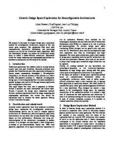
II. MPW Dicing and Reticle Floorplanning Fig. 1 shows an example of an MPW where 10 chips are placed on a reticle [5]. Forty replications of the same reticle are on the wafer, i.e., 40 layouts on the wafer per chip. However, with side-to-side dicing constraints (a dicing line starts from one side of a wafer and must stop at the other side of the wafer), we can not obtain the above number of bare dice because chips 6 and 7 will be destroyed and chip 1 will be discarded when dicing lines h2, h3, v1, and v2 are used to obtain chip 8. A good bare die considered in this paper is a die with four dicing lines located on its four borders, respectively, and without any other dicing lines across it. Two chips are said to be compatible if they can be good bare dice at the same time. The dicing lines used to obtain some good bare dice in a wafer (reticle) form a wafer (reticle) dicing plan. A wafer dicing problem can be formulated as follows: Given a reticle floorplan of N chips and the required production volume V p for chip p = 1..N , find the dicing plans for a minimal number of wafers such that the dicing outcomes can attain the production volumes of all chips. A dicing yield z k is defined as that at least z k V p good dice for each chip p must be obtained from dicing k wafers. The number of wafers for achieving the production volume is (1) Q = k ⎡1 z k ⎤ . The advantage of this dicing approach is that we need only decide the dicing plans for a few wafers and repeatedly apply these dicing plans to the rest of wafers. However, (1) gives only an upper bound on the number of needed wafers. A tighter lower bound is as follows.
(2) Q = ⎡k z k ⎤ This lower bound can be employed by the dicing method such as HVMIS-SA-Z to obtain a better solution [6]. Here, we will use HVMIS-SA-Z to perform wafer dicing. A reticle floorplanning problem is formulated as follows: Given a set of N chips and their required production volumes, decide the coordinates of the chips such that the number of wafers used to attain the required production volumes is minimized on the condition that no chips overlap and all chips are inside the reticle whose dimensions are not larger than maximally allowable values. The floorplanning objective function is very difficult to evaluate exactly if wafer dicing is not performed. In [5], the authors use compatibility to account for dicing yield during floorplanning. A higher compatibility score for a floorplan implies that more dice in the same reticle can be good at the same time. However, this does not necessarily mean that the floorplan would render a higher dicing yield. The number of reticles replicated in a wafer also plays an important role in getting higher dicing yield. Reticle size and compatibility are two competing factors that make reticle floorplanning a hard problem. Thus, in this paper we propose to explore the reticle floorplan design space to find an answer to this problem.
III. MPW Fabrication Cost Mask cost is mainly incurred by data preparation, mask write, mask inspection, etc [7]. Mask yield highly depends on the number of (very) critical layers used in a chip and the chip area. The materials used for mask tooling also incur a considerable portion of mask cost, especially for advanced technology nodes. The main contributors to wafer costs include exposure, hot process, etch, sputter, polish, etc [8]. Among them, exposure cost highly depends on the type of layers employed in a chip. An exposure on a very critical layer may cost as much as five times than an exposure on a non-critical layer [7]. Exposure cost also depends on the number of reticles on a wafer, i.e., depends on the wafer field size (equivalent to 1X reticle size). This part of cost is called field-size dependent cost in [9]. The part of wafer cost other than exposure cost is called field-size independent wafer cost. There are not too many MPW cost model found in the open literature [1,10]. The formulas given in MOSIS web site for calculating the cost based on chip area is in fact a pricing model which often includes a targeted profit margin. Based wafer
reticle(mask) h1 h2
h3
v2 v1 Good bare die
v3
Fig. 1. A multi-project wafer.
on our study, the price given in MOSIS web site is generally a piece-wise linear function of chip area for low and equal volume production. Several pricing models have been proposed in [11] to entice customers purchasing more reticle area with lower cost. The first MPW fabrication cost model is presented in [9]. This cost model includes two parts. The first part calculates the total MPW fabrication cost for a reticle floorplan with reticle area A, which is (3) T mpw ( A) = C m ( A) + Q ( A) C e ( A) + Q ( A) C w Where C m ( A) , C e (A) and C w are the mask cost, exposure cost per wafer, and field-size independent wafer cost, respectively; Q( A) is the number of wafers needed to satisfy volume requirements. The second part of the cost model [11] gives a formula to compute the cost assumed by each individual project. This cost model is generally correct except that it assumes the wafer exposure cost shared by a chip is inversely proportional to its area. This assumption causes an unfair share of cost, i.e., a smaller chip may pay more than a larger chip does for equal production volume. Here we present a revised formula to correct this deficiency. Given N chips whose areas and required production volumes are respectively A p and V p for p = 1..N , the cost assumed by chip p is C mpw ( p ) = C m ( A ) A p C e ( A )Q ( A )V p
∑ Ai +
i =1.. N
∑ V i + Q ( A )C w A p V p
i =1.. N
∑ Ai V i
(4)
i =1.. N
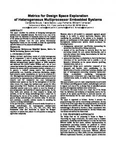
The first term is the share of mask cost, the second term is the share of exposure cost, and the third term is the share of field-size independent wafer cost. Our reasoning is that no matter how large a chip is, an exposure of a reticle will yield a copy of the chip. Therefore, exposure cost shared by a chip should be independent of chip area and is proportional to its production volume. We observe that a reasonable cost model should possess the following two properties: z A smaller chip should pay less than a larger chip if they have the same production volume. z A chip with larger production volume should pay more than a chip with smaller production volume if they have the same area. We need to check whether (4) possesses these two properties. We first obtain a reticle floorplan for the test case I6 (see TABLE II) using the SA approach presented in the next section. The dicing algorithm HVMIS-SA-Z [6] is used to obtain the number of wafers needed. All data used to compute the cost can be found in the experimental section. To check the first property, we arbitrarily set the required volume to 5500 dice per chip. As one can see from Fig. 2, the MPW fabrication cost is almost a linear function of chip area if the chips have same production volume. Thus, (4) possesses the first property. To check the second property, we scale up the volume requirement given in TABLE II by 50 times to make volume dependent cost more obvious. As one can see from Fig. 3, the chip with dimension (4.5,5.0) and the chip with dimension (6.5,3.5) have almost the same area, but
the later pays considerable more money for its fabrication owing to its larger volume. Thus, (4) also possesses the second property. From the cost point of view, we want mask cost as small as possible for small volume production, but for large volume production we want to balance the three cost factors in (3). Given a set of chips and their production volumes, what should their minimal-cost floorplan look like? This is a difficult question. As it was said previously, answering this question requires a design space exploration. To perform such a task, we need an efficient reticle floorplanner and dicing method. However, the reticle floorplanners found in the literature are either too restricted or too time consuming to prohibit design space exploration. Thus, we will present an efficient floorplanner in the next section.
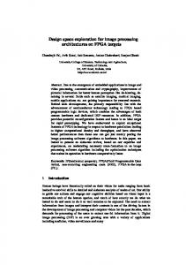
IV. Compatibility and Area Driven Floorplanner Our reticle floorplanner can adjust a coefficient to favor either reticle area minimization or compatibility maximization. It uses Simulated Annealing (SA) to place chips in a reticle which is divided into a matrix of grids as shown in Fig. 4, where W max and H max are maximum reticle width and height. Grids are sized to a number such that the boundary of a chip will align the grid lines when the chip is placed in the reticle. The objective function is ⎞ N −1⎛ N Max (1 − δ1 − δ 2 ) ∑ ⎜ ∑ E pq (V p + Vq ) ⎟ − δ1βWH − δ 2 β R ⎜ ⎟ p =1⎝ q = p +1 ⎠
(5)
Cost (X1000)
Where δ 1 + δ 2 ≤ 1 . The first term accounts for compatibility. It tries to maximize the compatibility among chips whose production volumes are large. The second term accounts for
150 100 50 0 0
20
40
60
reticle area which should be minimized. The third term accounts for chip overlap which should be eliminated to obtain a feasible solution. E pq is 1 if chips p and q are compatible in a reticle. Otherwise, E pq is 0. N is a normalizing factor; W and H β = ( N − 1)∑ p=1V p /(WmaxH max ) are reticle width and height, respectively; R is the total overlap area of chips. Our objective function is similar to the one used in the ILP model presented in [5]. The notable difference is that our objective function has a penalty on chip overlap. Allowing chip overlap during floorplanning would render SA more ropes to find better solutions. Four neighborhood structures are employed. z Move a chip to a new location. z Rotate a chip. z Move a chip and then rotate it. z Move a chip and align it with another chip. To move a chip, we randomly select a chip and then a legal location for that chip. Any move or rotation is prohibited if its change would place a chip outside a predefined maximum reticle area. The third neighborhood structure becomes the first one if rotation of a chip at its new location is prohibited. Basically, we don’t need the third neighborhood structure if we have the first two. Since we penalize chip overlap heavily to maintain a solution as feasible as possible, it is sometimes hard to place a chip at a location that first causes overlapping which is removed subsequently by a rotation. For example, as shown in Fig. 4, an attempt to move chip F to (0,3) might not be successful because of overlapping with chips C and E so that F has no chance being rotated at (0,3). However, the third neighborhood structure works just fine for this. A typical cooling schedule with cooling coefficient 0.95 is used. Simulated annealing is terminated when the best solution is not improved for a number of consecutive inner loops. The coefficient δ 2 for chip overlap is set to a very large number to avoid obtaining an infeasible solution. δ 1 can be adjusted to bias the optimization toward reticle minimization or compatibility maximization. This allows us to perform an exploration on reticle floorplan solution space. Our experiments show that the best floorplans obtained by the SA floorplanner is as good as or even better than those obtained by the approaches presented in [5].
2
Chip area (mm ) (Wmax,Hmax)
Fig. 2. Cost shared by chips with same production volume.
Cost(x1000)
A
(6.5, 3.5)
400 300
(4.5, 5.0)
B
C
200 100
E
(0,3)
0
D 0
20
40
60
2
Chip area (mm )
F
(0,0)
Fig. 3. Cost shared by chips with different production volumes. Fig. 4. Discretized reticle for floorplanning.
V. Space Exploration Methodology Here we propose a methodology to obtain a floorplan that would minimize the total MPW fabrication cost. The cost model proposed in Section III is used for cost calculation. This methodology consists of three steps: z Use the SA floorplanner presented in Section IV to perform design space exploration by varying the coefficient δ 1 from 0.000001 to 0.000009 with δ 2 =0.99999. z Employ the HVMIS-SA-Z dicing method [6] to perform wafer dicing for each floorplan. z Use the cost model to calculate the total fabrication cost based on the reticle size and the number of wafers used. The reticle floorplan incurring least total MPW fabrication cost is selected as the final solution. The cost assumed by each project is computed using (4) accordingly. An integrated tool that combines SA floorplanner, HVMIS-SA-Z dicing method, and MPW cost calculator has been implemented to facilitate design space exploration. Note that other robust and efficient floorplanners can also be used in our methodology as well.
volumes are key to the total fabrication cost. These data show that a good floorplan for I5 (I6) has a 47% (30%) saving in production cost with respect to a poor floorplan for small volume production and 41% (42%) saving for medium volume production. The time takes to perform such a design space exploration for a case is about 5 hours. Compared to the amount of cost saving, this overnight run is indeed a great pay-off. Once we have a reticle floorplan that results in minimum MPW fabrication cost, we can easily compute the cost assumed by each chip using (4). TABLE I Mask set cost for different wafer field sizes Wafer field 25*25 size 625 mm2 Mask cost
16*24 384 mm2
1,240,000
16*16 256 mm2
728,000
8*16 128 mm2
532,000
8*8 64 mm2
352,000
296,000
TABLE II Test cases (w, h | 1X required volume) Wmax=20 mm, Hmax=20 mm I5
(2.5,6.25 | 100|), (1.8,5.5 | 200), (2,1.25 | 300), (2.2,1.75 | 200), (1.7,2.25 | 200), (1.5,1.55 | 200), (2.3,3.75 | 200), (1,3.25 | 200), (1.3,4.25 | 80), (2.7, 1.1 | 60) (6.5, 6.5 | 60), (4.5, 5.0 | 100), (5.5, 1.5 | 120), (4.5, 3.0 | 120), (6.5, 3.5 | 160), (4.5, 3.5 | 160), (6.5, 8.0 | 200), (3.3, 3.5 | 200), (2.5, 3.5 | 200), (3.5, 2.5 | 200), (7.5, 2.5 | 200), (4.0, 2.5 | 200), (2.5, 2.5 | 200)
I6
VI. Experimental Results
Production cost (x100000)
8 Field-size independent wafer cost Exposure cost Mask cost
7 6 5 4 3 2 1 0 1
6
16
11
26 21 Floorplans
31
36
41
Fig. 5. MPW fabrication cost for I5 with 1X volume.
Field-size independent wafer cost Exposure cost Mask cost
30 Production cost (x100000)
In this section we perform a case study on the design space exploration using the methodology proposed in Section V. All experiments are done on a 1.8GHz 64-bit PC. Our study is made on 300 mm wafers. Although there exists much work about mask cost of ownership analysis, for simplicity we will use the mask cost data from [7]. These data given in TABLE I are calculated for 90nm technology node assuming that a chip has 8 very critical layers, 8 critical layers, and 12 non-critical layers. They are originally estimated for a reticle containing a number of dice of the same design with 8*8 mm2 wafer field size (equivalent to 1X reticle size). Note that the mask cost of MPW is somewhat underestimated due to underestimating its data preparation time and inspection time. We also use the data about cost per exposure in [7] to compute the exposure cost per wafer. The cost per exposure is $2.5 for very critical layer, $1.5 for critical layer, and $0.5 for non-critical layer. For the time being, we assume that wafer field-size independent wafer cost [12] is Cw=$2500. Two test cases in TABLE II obtained from the industry [13] are used in our experiments. These two test cases have drastically different characteristics. All chips in I5 have different dimensions with total chip area much smaller than the maximum reticle size. Many chips in I6 have same widths and heights with total chip area more than half the maximum reticle size. We use the method proposed in Section V to find a floorplan with minimum MPW fabrication cost. Figs. 5 and 6 show total MPW fabrication costs for different reticle floorplans for I5 with 1X and 50X volumes, respectively. Figs. 7 and 8 serve a similar purpose for I6. Each bar consists of mask cost, exposure cost, and field-size independent wafer cost. As shown in these figures, mask cost dominates the total wafer fabrication cost for low (1X) production volume. With larger (50X) production volume, exposure cost takes a lion share of the total cost so that the number of exposures per wafer and the number of wafers needed to satisfy production
25 20 15 10 5 0 1
6
11
16
21 26 Floorplans
31
36
Fig. 6. MPW fabrication cost for I5 with 50X volume.
41
8 Production cost (x100000)
observed that a higher dicing yield of many floorplans is mainly derived from more exposures per wafer. If we measure the yield per reticle exposure, the floorplans with a higher dicing yield are commonly seen to score low for this metric than those floorplans with a smaller dicing yield. This is especially true for I5. We have observed an instance for I5 that a floorplan with 1/3 of the reticle area, twice the dicing yield, and more than three times the number of exposures per wafer of another floorplan incurs 20% more cost. This gives the reason why the points in the center picture of Fig. 10 are spread much widely than those in Fig. 12. The degree of spreading highly depends on the underlying problem instance. Based on the above observations, it is clear that neither reticle area nor dicing yield can solely decide the total production cost, especially for large-volume production. Thus, performing a reticle floorplan design space exploration is required for finding a minimal-cost reticle floorplan.
Field-size independent wafer cost Exposure cost Mask cost
9
7 6 5 4 3 2 1 0 1
6
11
16
21 26 Floorplans
31
36
41
Fig. 7. MPW fabrication cost for I6 with 1X volume. Field-size independent wafer cost Exposure cost Mask cost
35
Production cost (x100000)
30
VII. Conclusions
25 20 15 10 5 0 1
6
11
16 21 26 Floorplans
31
36
41
Fig. 8. MPW fabrication cost for I6 with 50X volume.
Figs. 9 and 10 show the relations among reticle area, total fabrication cost, and dicing yield for I5 with 1X and 50X volume requirement, respectively. Figs. 11 and 12 serve a similar purpose for I6. Dicing yield is obtained from dicing three wafers at the same time. Normally, a smaller reticle corresponds to a higher dicing yield for I5, but this phenomenon is not that obvious for I6. Given the same reticle area, the dicing yields of different floorplans for I5 do not spread as widely as that for I6. This is due to the fact that the chips in I5 have different dimensions so that different floorplans within a given reticle area will not have a large difference in compatibility and thus in dicing yield. However, this is not true for I6 where the alignment of chip placement would make a bigger difference in dicing yield. For I5 with 1X production volume, the larger the yield, the smaller the cost. For I6 this is generally true, but a larger spread in production cost for the floorplans with the same yield is observed. Since mask cost dominates the total cost for low-volume production, it is the smaller reticle area rather than the higher yield that decides the total cost. This can be clearly observed from the data given in Figs. 9 and 11. Therefore, for low-volume production, the smaller the reticle area, the lower the total MPW fabrication cost. However, this does not always happen for 50X production volume. We have
This paper has presented a methodology to explore MPW reticle floorplan design space facilitated by a compatibility and area driven floorplaner. A new formula is introduced to compute the MPW fabrication cost assumed by each chip. It is shown that a good floorplan saves 47% production cost with respect to a poor floorplan for small volume production and saves 42% cost for medium volume production. Although reticle area generally corresponds well to production cost especially for small volume production, a design space exploration is strongly recommended for achieving minimal-cost production irregardless of volume requirements.
References [1] C. A. Pina, “MOSIS: IC prototyping and low volume production service,” Proc. of Intl. Conf. on Microelectronic Systems Education, 2001. [2] M. LaPedus. Is IC industry heading to the $10 million photomask?. Semiconductor Business News, Oct. 7, 2002. [3] A. B. Kahng, I. Mandoiu, Q. Wang, X. Xu, and A. Z. Zelikovsky, “Multi-project reticle floorplanning and wafer dicing,” Proc. of ISPD, pp.70-77, 2004 [4] G. Xu, R. Tian, D. Z. Pan, D.F. Wong, “A multi-objective floorplanner for shuttle mask,” Proc. of SPIE, vol 5567, pp. 340-350, 2004. [5] M. C. Wu and R. B. Lin, “Reticle floorplanning and wafer Dicing for Multiple Project Wafers,” ISQED, pp. 610-615, 2005. [6] M. C. Wu and R. B. Lin, “A comparative study on dicing of multiple project wafers,” IEEE Computer Society Annual Symposium on VLSI, pp. 314-315, 2005 [7] D. Pramanik, H. Kamberian, C. Progler, M. Sanie, and D. Pinto, “Cost effective strategies for ASIC masks,” Proc. of SPIE, vol. 5043, pp. 142-152, 2003. [8] S. Miraglia, C. Blouin, G. Boldman, S. Judd, T. Richardson, and D. Yao, “ABC modeling: advanced features,” Advanced Semiconductor Manufacturing Conf., pp. 336-339, 2002. [9] M. C. Wu and R. B. Lin, “Multiple project wafers for medium-volume IC production,” ISCAS, pp. 4725-4728, 2005.
[10] J. Bonn, S. Sisler, and P. Tivnan, “Balancing mask and lithography cost,” Advanced Semiconductor Manufacturing Conf., pp. 25-27, 2001. [11] T. Y. Yang, L. I. Tong, B. J.C. Yuan, "An innovative model of multi-project wafer service in the foundry industry," International
2.5
1 0.5 0 50
150
250
350
Production cost
2 1.5
7.5 7 6.5 6 5.5 5 4.5 4 3.5 3
x 100000
Dicing yield
3
Production cost
x 100000
3.5
Journal of Technology Management, Vol. 30, No.1/2 pp. 172 – 187, 2005. [12] “Optical lithography cost of ownership(COO) – Final Report for LITG501,” International SEMATECH. [13] Global UniChip, http://www.globalunichip.com
0.4 0.8 1.2 1.6
Reticle area (mm2)
2
7.5 7 6.5 6 5.5 5 4.5 4 3.5 3
2.4 2.8 3.2
50
150
250
350 2
Dcing yield
Reticle area (mm )
2.7 2.5 2.3
Production cost
5 Dicing yield
2.9
4 3 2 1 50
150
250
x 1000000
6
Production cost
7
x 1000000
x 0.01
Fig. 9. Area, yield, and cost for I5 with 1X volume.
2.1 1.9 1.7 1.5 1
350
2
2
3
Reticle area (mm )
4
5
2.9 2.7 2.5 2.3 2.1 1.9 1.7 1.5
6
Dicing yield
50
x 0.01
150
250
350
Reticle area (mm2)
Fig. 10. Area, yield, and cost for I5 with 50X volume.
0.8
7 6.5 6 5.5 5
Reticle area (mm2)
0.5
400
x 1000000
2.5 2 1.5 1 290
340
2
Reticle area (mm )
0.9
1.1
6.5 6 5.5 5 250
1.3
390
3.2 2.9 2.6 2.3 2 1.7 1
1.5
2
Dicing yield
2.5
3 x 0.01
Fig. 12. Area, yield, and cost for I6 with 50X volume.
300
350
400
Reticle area (mm2)
Dicing yield Fig. 11. Area, yield, and cost for I6 with 1X volume.
3
240
0.7
7
x 1000000
350
8
Production cost
300
Production cost
x 0.01
0.4 250
8.5 7.5
Production cost
1
0.6
Dicing yield
8 7.5
Production cost
Dicing yield
1.2
8.5
x 100000
x 100000
1.4
3.2 2.9 2.6 2.3 2 1.7 240
290
340
Reticle area (mm2)
390